US8036870B2 - Simulation method for efficient characterization of electronic systems under variability effects - Google Patents
Simulation method for efficient characterization of electronic systems under variability effects Download PDFInfo
- Publication number
- US8036870B2 US8036870B2 US12/144,524 US14452408A US8036870B2 US 8036870 B2 US8036870 B2 US 8036870B2 US 14452408 A US14452408 A US 14452408A US 8036870 B2 US8036870 B2 US 8036870B2
- Authority
- US
- United States
- Prior art keywords
- variability
- domain
- occurrence
- probability
- defining
- Prior art date
- Legal status (The legal status is an assumption and is not a legal conclusion. Google has not performed a legal analysis and makes no representation as to the accuracy of the status listed.)
- Active, expires
Links
Images


Classifications
-
- G—PHYSICS
- G06—COMPUTING OR CALCULATING; COUNTING
- G06F—ELECTRIC DIGITAL DATA PROCESSING
- G06F30/00—Computer-aided design [CAD]
- G06F30/30—Circuit design
- G06F30/32—Circuit design at the digital level
- G06F30/33—Design verification, e.g. functional simulation or model checking
- G06F30/3308—Design verification, e.g. functional simulation or model checking using simulation
- G06F30/3312—Timing analysis
-
- G—PHYSICS
- G06—COMPUTING OR CALCULATING; COUNTING
- G06F—ELECTRIC DIGITAL DATA PROCESSING
- G06F30/00—Computer-aided design [CAD]
- G06F30/30—Circuit design
- G06F30/32—Circuit design at the digital level
- G06F30/33—Design verification, e.g. functional simulation or model checking
- G06F30/3323—Design verification, e.g. functional simulation or model checking using formal methods, e.g. equivalence checking or property checking
-
- G—PHYSICS
- G06—COMPUTING OR CALCULATING; COUNTING
- G06F—ELECTRIC DIGITAL DATA PROCESSING
- G06F2111/00—Details relating to CAD techniques
- G06F2111/08—Probabilistic or stochastic CAD
Definitions
- the invention relates to method for simulating behavior of electronic systems under variability and deriving there from adaptations for the production process and/or measures to be taken within the electronic systems for guaranteeing proper performance irrespective of such variability.
- the method further relates to production processes capable of receiving and using information from the simulation method, electronic systems equipped with such performance guaranteeing methods, accepting and using information obtained with such simulation method.
- New tools enter the design flow to counter its impact, such as design for manufacturing (DFM), a collection of measures aiming to improve functional yield by correctly modeling and providing solutions for systematic manufacturing errors, and statistical static timing analysis (SSTA), and are used for the estimation of the impact of variability on parametric specifications, timing and leakage (see X.-W. Lin, B. Nikolic, P. Habitz, R. Radojcic, “Practical Aspects of Coping with Variability: An Electrical View”, Tutorial at ACM/IEEE Design Automation Conf. 2006; Y. Chen, A. Kahng, G. Robins, A. Zelikovsky, “Area Fill Synthesis for Uniform Layout Synthesis”, IEEE Trans. on CAD of Integrated Circuits and Systems, vol. 21, no. 10, pp.
- DFM design for manufacturing
- SSTA statistical static timing analysis
- Variability exhibits geometrical or spatial correlation: it may be local (as what is commonly known as “mismatch”) or global (“die to die”, “across wafer”, “wafer to wafer”), random e.g. due to Random Dopant Fluctuations, versus systematic, or non-reproducible versus reproducible.
- RDF random dopant fluctuations
- LER line edge roughness
- SSTA statistical static timing analysis
- SSTA also incorporate a statistical estimation of the leakage power consumption of the chip under variability (see R. Rao, A. Devgan, D. Blaauw, D. Sylvester, “Parametric yield estimation considering leakage Variability”, Proc. ACM/IEEE Design Automation Conference, pp. 442-447, 2004; M. Ashouei, A. Chatterjee, A. Singh, V. De, T. Mak, “Statistical estimation of correlated leakage power variation and its application to leakage-aware design”, Proc. Intl. Conf. on VLSI Design, 2006.) This provides the designer a partial view on the power consumption of the chip.
- Certain inventive aspects relate to simulation methods for determining behavior of electronic systems which are both accurate and efficient, meaning capable of giving reliable results without spending too much computation power, the methods being designed particularly by recognizing the particularities of variability (various types, correlated) in electronic systems and/or by incorporating the typical layered and/or hierarchical structure of such systems.
- an automated simulation method to be executed on a computer environment, for determining the behavior of electronic systems is provided, which includes the particularities of electronic system variability, in particular the fact simulation methods solely based on random selection of electronic system component variables in a Monte-Carlo based manner, will fail to include outlier values, which occur rarely but have a tremendous effect on the end result of the simulation.
- an automated simulation method to be executed on a computer environment, for determining the behavior of electronic systems is provided, which takes advantage of the typical layer and/or hierarchical structure of such systems, by propagating properties obtained for one level of the layer or hierarchy towards another level in an efficient way.
- an automated simulation method to be executed on a computer environment, for determining the behavior of electronic systems is provided, which recognizing the non-linear relations between the several layers, and selects in an automated way, how to combine the first and second aspect of the invention to find the final behavior again in an accurate but efficient way.
- a method for propagating variability up in “abstraction level” comprises defining a domain and population of possible values of at least one variability parameter each possible value of the at least one variability parameter having a probability of occurrence.
- the method further comprises performing a simulation to obtain the performance parameters of the output domain sample.
- the method further comprises aggregating the results of the individual computations into the parameter/variability.
- the method may further comprises condensing the number of possible values of at least one variability parameter by clustering a number of possible values and using a domain of these clustered values for randomly selecting inputs.
- a population in the method is reduced in size by combining (binning or clustering) nearby elements of the population into one single element with a average value of the constituting elements.
- the method may further comprise repeating the method of any of the previous claims over a plurality of abstraction levels.
- the exponent gamma [used at an abstraction level] is the same for all components inside the same EMC process.
- the output domain parameters and/or input domain parameters, and/or pointers to output domain or input domain parameters, for each item of the population, and optionally for items of a different populations are correlated with the item, are put in a table or plurality of tables, whereby items in the same line of the effective very table are correlated.
- the response surface model is a piece-wise linear model.
- FIG. 1 shows a Point-wise described distributions in one dimension.
- Top the result distribution of a “classic” Monte Carlo experiment: the list of entries equals the list of population members.
- Bottom “Exponent” Monte Carlo distribution.
- Members (“entries”) of the population have individual frequencies or “probabilities to occur in reality” (PTOIR).
- FIG. 2 is a diagram illustrating an example of a EMC set for a digital block.
- Three correlated object parameters are listed versus their frequency or “probability to occur in reality”.
- multiple such table can co-exists for different populations (e.g. a table for NANDs, a table for NORs, for a digital block etc.), which have the same number of rows in the table and for which the items on the same row number are correlated.
- This correlation can exist over abstraction level boundaries.
- the full system table might be correlated with the nMOSFET table.
- FIG. 4 is a diagram illustrating accuracy (average and overall +1 ⁇ and ⁇ 1 ⁇ ) of the estimation of the outlier fraction (OF) of NANDs versus the amount of samples in the population.
- ⁇ is 0.6.
- the theoretical outlier fraction is 0.04% (thick line).
- MC@1 ⁇ classic Monte Carlo
- FIG. 5 is a diagram illustrating exponent Monte Carlo experiments creating 100 random digital blocks. Each block contains 100 NANDs as from FIG. 3 .
- X-axis block delay
- Y-axis probability to occur in reality.
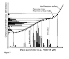
- FIG. 6 is a diagram illustrating a piece wise linear RSM for one dimensional input and output domains. Only the points that define the line pieces are actually simulated. All other points are obtained by evaluating the RSM. Hatched areas are superimposed distributions (PDFs) of the output and output domain parameters, as example.
- PDFs superimposed distributions
- FIG. 7 is a diagram illustrating a piece wise linear RSM for one dimensional input and output domains. Only the points that define the line pieces are actually simulated. All other points are obtained by evaluating the RSM. Superimposed on x (input domain) and y (output domain) axes are the distributions represented in the “EMC” style. From the input domain population, the white members are simulated, resulting in the point-wise RSM, the black members are evaluated using RSM.
- FIG. 8 is a diagram illustrating reduction of the number input domain points.
- Original populations are the small open circles. Points that are close together are combined in one by clustering (take one and discard the rest) or binning (make some weighted average). The resulting populations are the larger black circles.
- a method capable of handling variability over the whole manufacturing and design flow is proposed.
- the goal is propagating “almost any” variability distribution over all levels of abstraction that occur in a typical CMOS SoC design flow.
- the methodology builds on top of existing signoff and simulations flows, and “adds” or “enables” variability.
- EMC is proposed as a distribution which a way to represent any uni- or multi-dimensional distribution, be it coming from measurements or from analytical expressions.
- our framework we represent all “objects” with all their variability parameters in one large EMC table (See FIG. 2 ).
- such object can be a nMOSFET, in the simplest case with parameters Vth and Beta, or a NAND gate with parameters static power, dynamic energy, and delays for certain load conditions and input conditions (See FIG. 2 ).
- Monte Carlo experiments sampling such objects will automatically sample correlated parameters. Additional to that, correlation between objects—i.e. nMOSFETs are correlated to pMOSFETs, NAND delay is correlated to NOR delay, etc. as they share underlying common technology variability—is enabled by creating the EMC tables for each object concurrently, and implying correlation between the row indexes of the EMC table for each object.
- EMC provides also a sampling strategy for Monte Carlo experiments.
- FIG. 3 we show the results of a simple sampling experiment.
- Monte Carlo fails in tracing distributions tails and outliers. Entry sampling over-emphasizes them.
- EMC is a particular “variance reduction technique”, as in P. Bratley, B. Fox, L. Schrage, “A guide to simulation”, Springer-Verlag New-York 1983.
- FIG. 4 illustrates the efficiency of EMC to simulate distributions tails and outliers.
- NANDs are composed from MOSFETs that have 1/1e4 outliers.
- the outlier fraction estimates requires about 100 ⁇ less samples with EMC than with classic Monte Carlo. In this case, we are able to estimate the number of outliers with an accuracy of 1 sigma, using a 100 sample EMC population with a properly chosen ⁇ . This improvement is consistent with other observations; the factor depends on the actual outlier “rareness”, the ⁇ used, the number of components in the system (as MOSFETs in a NAND), and other peculiarities of the circuit.
- FIG. 5 represents a set of experiments creating larger random digital blocks from these random NANDs. Observe classic Monte Carlo and Entry Sampling fail in representing the full output distribution with main distributions, outliers and defect items. Good detail for the whole distribution is obtained when using a ⁇ between 0.1 and 0.4.
- Variability (variability parameters) is now expressed in the ability to execute the task and is then synonym to yield as a function of speed, power etc.
- input domain When raising the abstraction level up in the integrated circuit design and manufacturing flow, the “input domain” is the collection of possible values of the variability parameters of the lower abstraction level.
- the output domain is the collection of +possible values of the higher, resulting, abstraction level. e.g. in a Monte-Carlo or Monte-Carlo-like process
- PTOIR probability of occurrence
- FoO frequency of occurrence
- Probability of occurrence and PTOIR applies to individual members of the population or domain. Yet, they can apply to groups of elements of the population or regions of the domain. So can they apply to segments of an histogram, or can they be applied to a new population that is obtained by “binning” (combining multiple close by elements in one) an old population. It suffices to consider groups of elements in a population as an element themselves.
- PTS inputdomain ( PTOIR inputdomain ) (1 ⁇ )
- PTS inputdomain PTS classicmontecarlo ⁇ ( PTOIR inputdomain ) ( ⁇ )
- PTS enhancement ( PTOIR inputdomain ) ( ⁇ )
- the frequency of occurrence of the resulting element in the output domain is 1 (its PTOIR being frequency_of occurrence/population_size).
- the product to the PTS enhancement and the FoO outputdomain is for any value of gamma and for the classic Monte Carlo equal to 1.
- PTS enhancement and FoO outputdomain balance each other, hence no divergence from reality occurs, so the final result is accurate.
- EMC is a valid replacement of classic MC.
- EMC may converge must faster to the asymptotic result depending on the value chosen for gamma, as it will provide data on tails and outliers of the distribution faster, i.e. using less samples, requiring thus less CPU time for simulations.
- a method to create an output population of new_items by randomly sampling old_items of an input population, whereby the probability to sample and old_item is a function of the probability_to_exist_in_reality PTOIR (or FoO) of the old item, and the new PTOIR (or frequency of occurrence FoO) of the new_item is a complementary function of the PTOIRs of the n old_items.
- PTOIR or FoO
- E.g. take the case of an EMC experiment, creating a populations of NANDs, where by each NAND is composed of 4 randomly sampled MOSFETs, the where one is interested in is the variability of the NANDs being derived from the variability of the MOSFETs.
- the MOSFET variability can be expressed as (e.g., simplified, still realistic case) its Vth and beta; the input domain parameters are thus 8 in number and are the Vth and beta of each of the 4 transistors.
- the output information or what we want to obtain from the EMC experiment are (e.g., simplified but relevant) the delay and energy of the population of NANDS.
- the output domain parameters are thus 2 in number, being delay and energy of the NAND.
- a response surface model in order to have usability, should be a good approximation of its response surface.
- the simplest, and in fact most used response surface models are linear response surface, being in fact multidimensional planes in the input+output domain. Such approach is sometimes also called the “linear sensitivity method”.
- Most state of the art tools in electronic modeling use linear sensitivities if any.
- the advantage of the linear sensitivity is that it is a very simple linear analytic function, so that evaluation of the response surface model involves just a few CPU operations.
- Linear sensitivities are useful for evaluation of variability when the variability is small, so that a linear approximation around an average point is sufficiently correct.
- the response surface is strongly non linear so that linear surface models or linear responses are imperfect.
- the second aspect of invention is that these points in multidimensional space defining the RSM, are nothing else than a subset of the points in input and output domain of the EMC experiment.
- this decimation can be based on clustering or binning of the input domain points (figure UUU), namely, points that are close together (distance according to some metric, which we do not go in further detail here are many metrics can be envisaged), are combined in one point. That decimation can be light or severe. [Up to the point that we reduce the population to 1 (which is singular as then the response is just flat or nil), 2 (meaning that the response is a multidimensional line defied by two point, which may be of limited use), or a few.
- the RSM is a piece-wise linear interpolation (at the extremities extrapolation).
- an alternative is to first select those point of the RSM that are closest to the point needing evaluation by the RSM (“closest” in some metric, which we will not discuss further as many possibilities exists, such as relative distance, Euclidean distance, Mahalanobis distance etc.), and then suing these point to define a local multidimensional plane that can easily be evaluated for the point needing evaluation, again in a linear or non-linear interpolation fashion.
Landscapes
- Engineering & Computer Science (AREA)
- Computer Hardware Design (AREA)
- Physics & Mathematics (AREA)
- Theoretical Computer Science (AREA)
- Evolutionary Computation (AREA)
- Geometry (AREA)
- General Engineering & Computer Science (AREA)
- General Physics & Mathematics (AREA)
- Design And Manufacture Of Integrated Circuits (AREA)
Abstract
Description
-
- A systematic treatment of local versus global, systematic (reproducible) versus random (stochastic).
- Models need more detail than normal (Gaussian) distributions or linear sensitivities to small signals perturbation can offer. This is more true as perturbations become “large signal”, and distributions can have uncommon shapes.
- maintaining correlations of common underlying physical variability sources.
- The need to maintain a correlated view between speed performance and static/dynamic power, hence modeling the correlated variability of dynamic energy, static power and speed performance.
-
- 1. technology level, where variability (variability parameters) is expressed in concentration variations and small scale geometrical variations.
- 2. device level (transistor level, passive component level, interconnect level, compact model level), where variability (variability parameters) is the randomness of electrical parameters such as threshold voltage, resistance, capacitance etc
- 3. cell level (standard cell level, analog circuit level), where variability (variability parameters) is expressed as random variations of delay, speed, power, energy of the cell.
- 4. digital block level (which consists of a possibly hierarchical assembly of smaller blocks, up to full chip or integrated circuit level), where variability typically is expressed speed, power, energy, execution time. There are possibly several sub-abstraction levels inside this level, as digital blocks can be hierarchically organized.
- 5. system level, which is the digital block (or full integrated circuit, or mixed circuit blocks or ICs), PLUS the application and or software running on the digital block.
-
- having as output (as result) (a population of) cells, such as NAND-gate standard cells,
- using as input randomly picked MOSFETs, then
- the input samples are the MOSFETs. They are samples from the input population.
- The input abstraction level is the device level or compact model level, the input domain are the values of Vth (threshold voltage) of the picked MOSFETs. (there may be likely be more parameters in the input domain, theoretically all model parameters of the MOSFET could be input domain, but we simplify for the cause of this document)
- the output samples are NAND gates, forming together the output population. The output abstraction level is the cell level (or standard cell level), the output domain are the values of delay, power and energy of the created NAND gates. (there may be likely be more parameters in the output domain, in fact, all variable numbers in the so-called LIBERTY format representation of a standard cell are output domain parameters.
PTS inputdomain=(PTOIR inputdomain)(1−γ)
PTS inputdomain =PTS classicmontecarlo·(PTOIR inputdomain)(−γ)
Where we thus enhanced the PTS with a factor:
PTS enhancement=(PTOIR inputdomain)(−γ)
FoO outputdomain=(PTOIR inputdomain)(γ)
(understood that in a later step, FoO is normalized to PTIOR)
Yet its probability for that particular sample to be in the population has been enhanced by
PTS enhancement=(PTOIR inputdomain)(−γ)
-
- 1. how to select those point from the input domain to be used to create the RSM. And how to use also information of the output domain (after simulation) to optimize that choice.
- 2. how to evaluate the other point of the input domain, once the RSM is set up.
Selection of point of the input domain population to serve in the RSM.
Claims (11)
Priority Applications (1)
| Application Number | Priority Date | Filing Date | Title |
|---|---|---|---|
| US12/144,524 US8036870B2 (en) | 2007-06-22 | 2008-06-23 | Simulation method for efficient characterization of electronic systems under variability effects |
Applications Claiming Priority (2)
| Application Number | Priority Date | Filing Date | Title |
|---|---|---|---|
| US94589907P | 2007-06-22 | 2007-06-22 | |
| US12/144,524 US8036870B2 (en) | 2007-06-22 | 2008-06-23 | Simulation method for efficient characterization of electronic systems under variability effects |
Publications (2)
| Publication Number | Publication Date |
|---|---|
| US20090024378A1 US20090024378A1 (en) | 2009-01-22 |
| US8036870B2 true US8036870B2 (en) | 2011-10-11 |
Family
ID=39777024
Family Applications (2)
| Application Number | Title | Priority Date | Filing Date |
|---|---|---|---|
| US12/144,491 Expired - Fee Related US8286112B2 (en) | 2007-06-22 | 2008-06-23 | Methods for characterization of electronic circuits under process variability effects |
| US12/144,524 Active 2029-09-21 US8036870B2 (en) | 2007-06-22 | 2008-06-23 | Simulation method for efficient characterization of electronic systems under variability effects |
Family Applications Before (1)
| Application Number | Title | Priority Date | Filing Date |
|---|---|---|---|
| US12/144,491 Expired - Fee Related US8286112B2 (en) | 2007-06-22 | 2008-06-23 | Methods for characterization of electronic circuits under process variability effects |
Country Status (2)
| Country | Link |
|---|---|
| US (2) | US8286112B2 (en) |
| EP (1) | EP2006784A1 (en) |
Cited By (2)
| Publication number | Priority date | Publication date | Assignee | Title |
|---|---|---|---|---|
| US8589842B1 (en) * | 2012-11-09 | 2013-11-19 | International Business Machines Corporation | Device-based random variability modeling in timing analysis |
| US9208271B1 (en) * | 2010-11-19 | 2015-12-08 | Cadence Design Systems, Inc. | Transaction correlation system |
Families Citing this family (103)
| Publication number | Priority date | Publication date | Assignee | Title |
|---|---|---|---|---|
| GB2443277B (en) * | 2006-10-24 | 2011-05-18 | Advanced Risc Mach Ltd | Performing diagnostics operations upon an asymmetric multiprocessor apparatus |
| CN105426567B (en) * | 2007-03-09 | 2018-12-07 | 明导公司 | Incremental analysis of layout design data |
| EP2006784A1 (en) * | 2007-06-22 | 2008-12-24 | Interuniversitair Microelektronica Centrum vzw | Methods for characterization of electronic circuits under process variability effects |
| US20090013292A1 (en) * | 2007-07-03 | 2009-01-08 | Mentor Graphics Corporation | Context dependent timing analysis and prediction |
| US7991577B2 (en) * | 2007-08-30 | 2011-08-02 | HSB Solomon Associates, LLP | Control asset comparative performance analysis system and methodology |
| US7752585B2 (en) * | 2007-10-15 | 2010-07-06 | International Business Machines Corporation | Method, apparatus, and computer program product for stale NDR detection |
| US8245084B2 (en) * | 2008-01-11 | 2012-08-14 | International Business Machines Corporation | Two-level representative workload phase detection |
| US8204730B2 (en) * | 2008-06-06 | 2012-06-19 | Synopsys, Inc. | Generating variation-aware library data with efficient device mismatch characterization |
| US8825464B2 (en) * | 2008-09-02 | 2014-09-02 | Oracle America, Inc. | Method and apparatus for parallelization of sequential power simulation |
| JP2010160787A (en) * | 2008-12-11 | 2010-07-22 | Jedat Inc | System for creating parameter information, system for estimating yields, program and recording medium |
| US8161434B2 (en) | 2009-03-06 | 2012-04-17 | Synopsys, Inc. | Statistical formal activity analysis with consideration of temporal and spatial correlations |
| US8201137B1 (en) * | 2009-03-06 | 2012-06-12 | Cadence Design Systems, Inc. | Method and apparatus for AMS simulation of integrated circuit design |
| US20100250187A1 (en) * | 2009-03-25 | 2010-09-30 | Imec | Method and system for analyzing performance metrics of array type circuits under process variability |
| US8122411B2 (en) * | 2009-07-16 | 2012-02-21 | International Business Machines Corporation | Method of performing static timing analysis considering abstracted cell's interconnect parasitics |
| DE102009034242A1 (en) * | 2009-07-22 | 2011-01-27 | Volkswagen Ag | Method for testing controller utilized for controlling e.g. brake lamp of lorry, involves automatically operating regulator to determine whether controller properly operates or not upon detected output signal |
| US9684742B1 (en) * | 2009-08-26 | 2017-06-20 | Altera Corporation | Method and apparatus for performing timing analysis on calibrated paths |
| JP5445066B2 (en) * | 2009-11-25 | 2014-03-19 | 富士通株式会社 | Analysis support program, analysis support apparatus, and analysis support method |
| US8924902B2 (en) * | 2010-01-06 | 2014-12-30 | Qualcomm Incorporated | Methods and circuits for optimizing performance and power consumption in a design and circuit employing lower threshold voltage (LVT) devices |
| US20110181331A1 (en) * | 2010-01-24 | 2011-07-28 | Freescale Semiconductor, Inc. | Integrated circuit with leakage reduction in static nets |
| US8407646B2 (en) * | 2010-02-11 | 2013-03-26 | Synopsys, Inc. | Active net and parasitic net based approach for circuit simulation and characterization |
| US8266569B2 (en) * | 2010-03-05 | 2012-09-11 | Advanced Micro Devices, Inc. | Identification of critical enables using MEA and WAA metrics |
| JP5370256B2 (en) * | 2010-05-06 | 2013-12-18 | 富士通株式会社 | Analysis support program, analysis support apparatus, and analysis support method |
| JP2011237989A (en) * | 2010-05-10 | 2011-11-24 | Toshiba Corp | Apparatus for designing semiconductor integrated circuit, and method and program for designing the same |
| US8515724B2 (en) * | 2010-06-22 | 2013-08-20 | International Business Machines Corporation | Technology computer-aided design (TCAD)-based virtual fabrication |
| WO2012039847A2 (en) * | 2010-08-09 | 2012-03-29 | Charter Ip Llc | Method and system of converting timing reports into timing waveforms |
| US8522182B2 (en) * | 2011-03-21 | 2013-08-27 | International Business Machines Corporation | Generation of an end point report for a timing simulation of an integrated circuit |
| US9235675B2 (en) * | 2011-04-01 | 2016-01-12 | Taiwan Semiconductor Manufacturing Company, Ltd. | Multidimensional monte-carlo simulation for yield prediction |
| US20120266123A1 (en) * | 2011-04-12 | 2012-10-18 | Texas Instruments Incorporated | Coherent analysis of asymmetric aging and statistical process variation in electronic circuits |
| US8555210B2 (en) | 2011-04-29 | 2013-10-08 | Micron Technology, Inc. | Systems and methods for stochastic models of mask process variability |
| US8811068B1 (en) | 2011-05-13 | 2014-08-19 | Suvolta, Inc. | Integrated circuit devices and methods |
| US8397197B1 (en) | 2011-05-25 | 2013-03-12 | Applied Micro Circuits Corporation | Integrated circuit module time delay budgeting |
| US20130046912A1 (en) * | 2011-08-18 | 2013-02-21 | Maxeler Technologies, Ltd. | Methods of monitoring operation of programmable logic |
| US9355000B1 (en) * | 2011-08-23 | 2016-05-31 | The Mathworks, Inc. | Model level power consumption optimization in hardware description generation |
| US8392860B1 (en) | 2011-09-01 | 2013-03-05 | Apple Inc. | Identifying speed binning test vectors during simulation of an integrated circuit design |
| US8650519B2 (en) * | 2011-09-01 | 2014-02-11 | Apple Inc. | Automated functional coverage for an integrated circuit design |
| US8499274B2 (en) * | 2011-11-30 | 2013-07-30 | Taiwan Semiconductor Manufacturing Co., Ltd. | Computer implemented system and method for leakage calculation |
| US8819603B1 (en) | 2011-12-15 | 2014-08-26 | Suvolta, Inc. | Memory circuits and methods of making and designing the same |
| US8739094B2 (en) * | 2011-12-22 | 2014-05-27 | Lsi Corporation | Power estimation using activity information |
| US8543953B2 (en) | 2012-01-04 | 2013-09-24 | Apple Inc. | Automated stimulus steering during simulation of an integrated circuit design |
| US8522181B2 (en) | 2012-01-24 | 2013-08-27 | Synopsys, Inc. | Capacitance extraction for advanced device technologies |
| US9183330B2 (en) * | 2012-01-31 | 2015-11-10 | Mentor Graphics Corporation | Estimation of power and thermal profiles |
| US8413095B1 (en) * | 2012-02-21 | 2013-04-02 | International Business Machines Corporation | Statistical single library including on chip variation for rapid timing and power analysis |
| US9411921B2 (en) | 2012-04-27 | 2016-08-09 | Globalfoundries Inc. | FET-bounding for fast TCAD-based variation modeling |
| EP2662791A1 (en) * | 2012-05-11 | 2013-11-13 | Stichting IMEC Nederland | A method and apparatus for monitoring timing of cricital paths |
| US9977849B2 (en) * | 2013-01-09 | 2018-05-22 | Nxp Usa, Inc. | Method and apparatus for calculating delay timing values for an integrated circuit design |
| US8819605B1 (en) * | 2013-03-06 | 2014-08-26 | Oracle International Corporation | Deriving effective corners for complex correlations |
| US9038006B2 (en) * | 2013-04-30 | 2015-05-19 | Freescale Semiconductor, Inc. | Method and apparatus for generating gate-level activity data for use in clock gating efficiency analysis |
| JP6111880B2 (en) * | 2013-06-11 | 2017-04-12 | 富士通株式会社 | Verification support method, verification support program, and verification support apparatus |
| CN104598659B (en) | 2013-10-31 | 2018-09-18 | 格芯公司 | The method and apparatus that digital circuit is emulated |
| US9817931B1 (en) | 2013-12-05 | 2017-11-14 | The Mathworks, Inc. | Systems and methods for generating optimized hardware descriptions for models |
| US10078717B1 (en) | 2013-12-05 | 2018-09-18 | The Mathworks, Inc. | Systems and methods for estimating performance characteristics of hardware implementations of executable models |
| EP2899654A1 (en) * | 2014-01-28 | 2015-07-29 | IMEC vzw | Method, system and computer program product for characterizing the variability of an integrated circuit design |
| US9262569B2 (en) | 2014-02-20 | 2016-02-16 | Globalfoundries Inc. | Balancing sensitivities with respect to timing closure for integrated circuits |
| US9311444B1 (en) * | 2014-07-10 | 2016-04-12 | Sandia Corporation | Integrated circuit test-port architecture and method and apparatus of test-port generation |
| US9760672B1 (en) | 2014-12-22 | 2017-09-12 | Qualcomm Incorporated | Circuitry and method for critical path timing speculation to enable process variation compensation via voltage scaling |
| US9710590B2 (en) * | 2014-12-31 | 2017-07-18 | Arteris, Inc. | Estimation of chip floorplan activity distribution |
| KR102324782B1 (en) * | 2015-01-22 | 2021-11-11 | 삼성전자주식회사 | Method of performing static timing analysis for an integrated circuit |
| US20160283629A1 (en) | 2015-03-27 | 2016-09-29 | Imec Vzw | Complexity-reduced simulation of circuit reliability |
| US9564884B1 (en) * | 2015-04-13 | 2017-02-07 | Qualcomm Incorporated | Circuitry and method for measuring negative bias temperature instability (NBTI) and hot carrier injection (HCI) aging effects using edge sensitive sampling |
| US9536038B1 (en) | 2015-04-13 | 2017-01-03 | Qualcomm Incorporated | Method and algorithm for functional critical paths selection and critical path sensors and controller insertion |
| US9564883B1 (en) * | 2015-04-13 | 2017-02-07 | Qualcomm Incorporated | Circuitry and method for timing speculation via toggling functional critical paths |
| US9507891B1 (en) | 2015-05-29 | 2016-11-29 | International Business Machines Corporation | Automating a microarchitecture design exploration environment |
| US9697310B2 (en) * | 2015-11-02 | 2017-07-04 | Winbond Electronics Corporation | Level faults interception in integrated circuits |
| US10375325B2 (en) * | 2016-06-23 | 2019-08-06 | Fluke Corporation | Thermal anomaly detection |
| US10185795B1 (en) | 2016-10-11 | 2019-01-22 | Cadence Design Systems, Inc. | Systems and methods for statistical static timing analysis |
| US10073934B1 (en) * | 2016-10-11 | 2018-09-11 | Cadence Design Systems, Inc. | Systems and methods for statistical static timing analysis |
| WO2018118078A1 (en) | 2016-12-23 | 2018-06-28 | Google Inc. | Integrated circuit design system and method |
| US10732703B2 (en) | 2017-03-02 | 2020-08-04 | Futurewei Technologies, Inc. | Apparatus and method for reducing an energy consumption of hardware based on an application state |
| CN108694261A (en) * | 2017-04-10 | 2018-10-23 | 中国石油天然气股份有限公司 | Method and device for constructing equipment model |
| CN117272924A (en) * | 2017-04-28 | 2023-12-22 | 三星电子株式会社 | How to design integrated circuits |
| KR102402673B1 (en) * | 2017-04-28 | 2022-05-26 | 삼성전자주식회사 | Computer-implemented method and computing system for designing integrated circuit by considering process variations of Back-End-Of-Line |
| US10621296B1 (en) | 2017-06-07 | 2020-04-14 | Synopsys, Inc. | Generating SAIF efficiently from hardware platforms |
| US10546095B2 (en) * | 2017-06-13 | 2020-01-28 | International Business Machines Corporation | Parameter collapsing and corner reduction in an integrated circuit |
| US11113442B2 (en) * | 2017-09-28 | 2021-09-07 | Intel Corporation | Methods and apparatus for reducing reliability degradation on an integrated circuit |
| CN111587378B (en) | 2017-11-15 | 2023-04-04 | 普罗泰克斯公司 | Integrated circuit margin measurement and failure prediction apparatus |
| US12282058B2 (en) | 2017-11-23 | 2025-04-22 | Proteantecs Ltd. | Integrated circuit pad failure detection |
| WO2019102467A1 (en) | 2017-11-23 | 2019-05-31 | Proteantecs Ltd. | Integrated circuit pad failure detection |
| WO2019135247A1 (en) | 2018-01-08 | 2019-07-11 | Proteantecs Ltd. | Integrated circuit workload, temperature and/or sub-threshold leakage sensor |
| US11740281B2 (en) | 2018-01-08 | 2023-08-29 | Proteantecs Ltd. | Integrated circuit degradation estimation and time-of-failure prediction using workload and margin sensing |
| TWI828676B (en) | 2018-04-16 | 2024-01-11 | 以色列商普騰泰克斯有限公司 | Methods for integrated circuit profiling and anomaly detection and relevant computer program products |
| TWI681311B (en) * | 2018-04-27 | 2020-01-01 | 瑞昱半導體股份有限公司 | Circuit design system and checking method |
| TWI796494B (en) * | 2018-06-19 | 2023-03-21 | 以色列商普騰泰克斯有限公司 | Efficient integrated circuit simulation and testing |
| CN109101239B (en) * | 2018-08-30 | 2021-09-14 | 杭州电子科技大学 | Standard answer generation method of online Verilog code automatic judgment system |
| TWI697797B (en) * | 2018-11-08 | 2020-07-01 | 瑞昱半導體股份有限公司 | Method for determining voltage of integrated circuit and finding relation between voltage and circuit parameter |
| US10740262B2 (en) | 2018-12-30 | 2020-08-11 | Proteantecs Ltd. | Integrated circuit I/O integrity and degradation monitoring |
| US10796046B2 (en) * | 2019-01-18 | 2020-10-06 | Mentor Graphics Corporation | Machine learning-based parasitic extraction automation for circuit design and verification |
| US11580356B2 (en) * | 2019-07-19 | 2023-02-14 | Qualcomm Incorporated | Efficient inferencing with piecewise pointwise convolution |
| US11763046B2 (en) * | 2019-11-05 | 2023-09-19 | Autodesk, Inc. | Techniques for automatically selecting simulation tools for and performing related simulations on computer-generated designs |
| EP4070315A4 (en) | 2019-12-04 | 2023-11-29 | Proteantecs Ltd. | MONITORING DEGRADATION OF A MEMORY DEVICE |
| US11126769B2 (en) * | 2020-02-04 | 2021-09-21 | Applied Materials, Inc. | Unified material-to-systems simulation, design, and verification for semiconductor design and manufacturing |
| US11275883B2 (en) | 2020-02-12 | 2022-03-15 | Siemens Industry Software Inc. | Machine learning-based classification in parasitic extraction automation for circuit design and verification |
| IL297427A (en) | 2020-04-20 | 2022-12-01 | Proteantecs Ltd | Inter-chip connectivity monitoring |
| EP4176276A4 (en) | 2020-07-06 | 2024-08-07 | Proteantecs Ltd. | INTEGRATED CIRCUIT MARGIN MEASUREMENT FOR STRUCTURAL TEST |
| US12470223B2 (en) | 2021-04-07 | 2025-11-11 | Proteantecs Ltd. | Adaptive frequency scaling based on clock cycle time measurement |
| TWI783773B (en) * | 2021-11-10 | 2022-11-11 | 瑞昱半導體股份有限公司 | Method for establishing variation model related to circuit characteristics for performing circuit simulation, and associated circuit simulation system |
| CN114239436B (en) * | 2021-12-28 | 2025-07-08 | 中山大学 | Pool boiling numerical simulation method for randomly distributed hydrophobic points |
| US11842132B1 (en) * | 2022-03-09 | 2023-12-12 | Synopsys, Inc. | Multi-cycle power analysis of integrated circuit designs |
| US11815551B1 (en) | 2022-06-07 | 2023-11-14 | Proteantecs Ltd. | Die-to-die connectivity monitoring using a clocked receiver |
| US12481811B1 (en) * | 2022-12-05 | 2025-11-25 | Cadence Design Systems, Inc. | Circuit design modification based on timing tradeoff |
| US12013800B1 (en) | 2023-02-08 | 2024-06-18 | Proteantecs Ltd. | Die-to-die and chip-to-chip connectivity monitoring |
| US12123908B1 (en) | 2023-09-12 | 2024-10-22 | Proteantecs Ltd. | Loopback testing of integrated circuits |
| WO2025085076A1 (en) * | 2023-10-17 | 2025-04-24 | Siemens Industry Software Inc. | Evaluating power dissipation |
| US12461143B2 (en) | 2024-01-24 | 2025-11-04 | Proteantecs Ltd. | Integrated circuit margin measurement |
Citations (8)
| Publication number | Priority date | Publication date | Assignee | Title |
|---|---|---|---|---|
| US6880136B2 (en) | 2002-07-09 | 2005-04-12 | International Business Machines Corporation | Method to detect systematic defects in VLSI manufacturing |
| US6888564B2 (en) | 2002-05-24 | 2005-05-03 | Koninklijke Philips Electronics N.V. | Method and system for estimating sharpness metrics based on local edge kurtosis |
| EP1583009A1 (en) | 2004-03-30 | 2005-10-05 | Interuniversitair Micro-Elektronica Centrum | Method and apparatus for designing and manufacturing electronic circuits subject to process variations |
| US20070098116A1 (en) * | 2005-10-31 | 2007-05-03 | Lg Electronics Inc. | Apparatus for performing initial synchronization and frame synchronization in mobile communications system and method thereof |
| US20070277134A1 (en) | 2006-05-25 | 2007-11-29 | Lizheng Zhang | Efficient statistical timing analysis of circuits |
| US20080005707A1 (en) | 2006-06-28 | 2008-01-03 | Interuniversitair Microelektronica Centrum Vzw (Imec) | Method for exploring feasibility of an electronic system design |
| US20080046692A1 (en) | 2006-08-16 | 2008-02-21 | Gerald Paul Michalak | Method and Apparatus for Executing Processor Instructions Based on a Dynamically Alterable Delay |
| US7539893B1 (en) | 2005-09-16 | 2009-05-26 | Pmc-Sierra, Inc. | Systems and methods for speed binning of integrated circuits |
Family Cites Families (4)
| Publication number | Priority date | Publication date | Assignee | Title |
|---|---|---|---|---|
| US7474999B2 (en) * | 2002-12-23 | 2009-01-06 | Cadence Design Systems, Inc. | Method for accounting for process variation in the design of integrated circuits |
| JP2004252831A (en) * | 2003-02-21 | 2004-09-09 | Matsushita Electric Ind Co Ltd | LSI statistical delay simulation apparatus and simulation method thereof |
| US7725848B2 (en) * | 2005-01-27 | 2010-05-25 | Wolfgang Nebel | Predictable design of low power systems by pre-implementation estimation and optimization |
| EP2006784A1 (en) * | 2007-06-22 | 2008-12-24 | Interuniversitair Microelektronica Centrum vzw | Methods for characterization of electronic circuits under process variability effects |
-
2008
- 2008-06-20 EP EP08158713A patent/EP2006784A1/en not_active Withdrawn
- 2008-06-23 US US12/144,491 patent/US8286112B2/en not_active Expired - Fee Related
- 2008-06-23 US US12/144,524 patent/US8036870B2/en active Active
Patent Citations (8)
| Publication number | Priority date | Publication date | Assignee | Title |
|---|---|---|---|---|
| US6888564B2 (en) | 2002-05-24 | 2005-05-03 | Koninklijke Philips Electronics N.V. | Method and system for estimating sharpness metrics based on local edge kurtosis |
| US6880136B2 (en) | 2002-07-09 | 2005-04-12 | International Business Machines Corporation | Method to detect systematic defects in VLSI manufacturing |
| EP1583009A1 (en) | 2004-03-30 | 2005-10-05 | Interuniversitair Micro-Elektronica Centrum | Method and apparatus for designing and manufacturing electronic circuits subject to process variations |
| US7539893B1 (en) | 2005-09-16 | 2009-05-26 | Pmc-Sierra, Inc. | Systems and methods for speed binning of integrated circuits |
| US20070098116A1 (en) * | 2005-10-31 | 2007-05-03 | Lg Electronics Inc. | Apparatus for performing initial synchronization and frame synchronization in mobile communications system and method thereof |
| US20070277134A1 (en) | 2006-05-25 | 2007-11-29 | Lizheng Zhang | Efficient statistical timing analysis of circuits |
| US20080005707A1 (en) | 2006-06-28 | 2008-01-03 | Interuniversitair Microelektronica Centrum Vzw (Imec) | Method for exploring feasibility of an electronic system design |
| US20080046692A1 (en) | 2006-08-16 | 2008-02-21 | Gerald Paul Michalak | Method and Apparatus for Executing Processor Instructions Based on a Dynamically Alterable Delay |
Non-Patent Citations (57)
| Title |
|---|
| Agarwal et al., Process variation in embedded memories: failure analysis and variation aware architecture, IEEE Journal of Solid-State Circuits (Sep. 2005), vol. 40 No. 9:1804-1814. |
| Agarwal et al., Statistical timing analysis using bounds and selective enumeration, IEEE Trans. on CAD (Sep. 2003), vol. 22 No. 9. |
| Antreich et al., Circuit analysis and optimization driven by worst-case distances, IEEE Trans. on CAD (Jan. 1994), vol. 13, No. 1. |
| ARM The Architecture for the Digital World, http://www.arm.com/products/physical-ip/embedded-memory-ip/index.php, accessed Feb. 21, 2011. |
| Ashouei et al, Statistical Estimation of Correlated Leakage Power Variation and Its Application to Leakage-Aware Design, Proceedings of 19th International Conference on VLSI Design, Jan. 3-7, 2006, 7 pages. |
| Ashouei et al, Statistical Estimation of Correlated Leakage Power Variation and Its Application to Leakage—Aware Design, Proceedings of 19th International Conference on VLSI Design, Jan. 3-7, 2006, 7 pages. |
| Austin et al., Making typical silicon matter with razor, IEEE Computer (Mar. 2004) pp. 57-65. |
| Benini et al., System-level power optimization techniques and tools, ACM Trans. on Design Automation for Embedded Systems, vol. 5, Issue 2, Apr. 2000, pp. 288-293. |
| Blaauw et al., CAD tools for variation tolerance, Design Automation Conference (Jun. 2005), 766. |
| Borkar, Designing reliable systems from unreliable components: the challenges of transistor variability and degradation, IEEE Micro (Nov./Dec. 2005), vol. 25, No. 6, pp. 10-16. |
| Bratley et al., A Guide to Simulation, 1983, pp. 42-72, Springer-Verlag New York Inc., New York. |
| Chang et al., Statistical timing analysis considering spatial correlations using a single PERT-like traversal, Intl. Conf. on Computer Aided Design (Nov. 11-13, 2003), pp. 621-625. |
| Chen et al, Area Fill Synthesis for Uniform Layout Density, IEEE Transactions on Computer-Aided Design of Integrated Circuits and Systems, Oct. 2002, vol. 21, No. 10, pp. 1132-1147. |
| Clark et al., The Greatest of a Finite Set of Random Variables, Operations Research, Mar.-Apr. 1961, vol. 9, No. 2, pp. 145-162. |
| Dierickx et al., "VAM IF" Variability and Reliability Aware Modeling Information Format Definition and User Manual, Jul. 2007. |
| Dierickx et al., Propagating Variability from Technology to System Level, 2007. * |
| European Search Report dated Oct. 22, 2007 in European Application 07075505.3. |
| Genest et al., Everything you always wanted to know about copula modeling but were afraid to ask, Journal of Hydrologic Engineering (Mar. 21, 2006). |
| Grobman et al, Reticle Enhancement Technology: Implications and Challenges for Physical Design, 38th Conference on Design Automation, DAC Jun. 18-22, 2001, pp. 72-78, Las Vegas, Nevada. |
| Gupta et al, Manufacturing-Aware Physical Design, IEEE/ACM Int'l Conference on Computer-Aided Design, ICCAD Nov. 11-13, 2003, pp. 681-687, San Jose, California. |
| Gupta et al, Toward a Systematic-Variation Aware Timing Methodology, Design Automation Conference, Jun. 7-11, 2004, pp. 321-326, San Jose, California. |
| Gupta, et al, Toward Performance-Driven Reduction of the Cost of RET-Based Lithography Control, Proc. SPIE, Conference date: Feb. 27, 2003, Online publication date: Jul. 31, 2003, vol. 5043, No. 123. |
| Habitz, P., Chip Timing and Optimization using Statistical Analysis Methods, ASICs Timing Methodology, from Practical Aspects of Coping with Variability: An Electrical View, Tutorial at ACM/IEEE Design Automation Conf. Jul. 24-28, 2006. |
| Hong et al., On-line scheduling of hard real-time tasks on variable voltage processors, Intl. Conf. on Computer Aided Design (Nov. 1998), pp. 653-656, San Jose, CA. |
| International Technology Roadmap for Semiconductors, http://public.itrs.net, 2005. |
| Jacobs et al, Gate Sizing Using a Statistical Delay Model, Design Automation and Test in Europe Conference and Exhibition, Mar. 27-30, 2000. |
| Kim et al., TCAD-Based Statistical Analysis and Modeling of Gate Line-Edge Roughness Effect on Nanoscale MOS Transistor Performance and Scaling, IEEE Transactions on Semiconductor Manufacturing, May 2004, vol. 17, No. 2, pp. 192-200. |
| Lin, X.W., Design and Process Variability-the Source and Mechanisms, from Practical Aspects of Coping with Variability: An Electrical View, Tutorial at ACM/IEEE Design Automation Conf. Jul. 24-28, 2006. |
| Lin, X.W., Design and Process Variability—the Source and Mechanisms, from Practical Aspects of Coping with Variability: An Electrical View, Tutorial at ACM/IEEE Design Automation Conf. Jul. 24-28, 2006. |
| Mani et al., A new statistical optimization algorithm for gate sizing, Intl. Conf. on Computer Design (Oct. 11-13, 2004), pp. 272-277. |
| Mani et al., An efficient algorithm for statistical minimization of total power under timing yield constraints, Design Automation Conference (Jun. 13-17, 2005), pp. 309-314, Anaheim, CA. |
| Montgomery, Applied statistics & probability for engineers, Chapter 5: Joint Probability Distributions, John Wiley & Sons, Jan. 1994. |
| Nikolic, B., Capturing Variability, from Practical Aspects of Coping with Variability: An Electrical View, Tutorial at ACM/IEEE Design Automation Conf. Jul. 24-28, 2006. |
| Nose et al. Vth-hopping scheme to reduce subthreshold leakage for low-power processors, IEEE J. of Solid-State Circuits (Mar. 2002), vol. 37 No. 3, pp. 413-419. |
| Office Action dated Dec. 2, 2010 in U.S. Appl. No. 11/769,546. |
| Office Action dated Jul. 21, 2010 in U.S. Appl. No. 11/769,546. |
| Office Action dated Nov. 10, 2009 in U.S. Appl. No. 11/769,546. |
| Okuma et al. Real-time task scheduling for a variable voltage processor, Intl. Symposium on System Synthesis (Nov. 1999), 24-29. |
| Papanikolaou et al., A system-level methodology for fully compensating process variability impact of memory organizations in periodic applications, Intl. Conference on HW/SW Co-design and System Synthesis (CODES+ISSS) (Sep. 19-21, 2005) New Jersey, USA. |
| Patel et al., Synthesis of partitioned shared memory architectures for energy-sufficient multi-processor SoC, Proceedings of the Conference on Design, Automation and Test in Europe, Feb. 16-20, 2004, pp. 700-701. |
| Pelgrom et al. Matching Properties of MOS Transistors, IEEE Journal of Solid-State Circuits, Oct. 1989, vol. 24, No. 5, pp. 1433-1440. |
| Rao et al, Parametric Yield Estimation Considering Leakage Variability, Annual ACM IEEE Design Automation Conference, Jun. 7-11, 2004, pp. 442-447, San Diego, California. |
| Riko, R., DFM View, Methodology Perspectives, Techniques for Stitching Together DFM Methods and Timing Optimization into a Usable Methodology, from Practical Aspects of Coping with Variability: An Electrical View, Tutorial at ACM/IEEE Design Automation Conf. Jul. 24-28, 2006. |
| Sinha et al., Advances in Computation of the Maximum of a Set of Random Variables, Proceedings of the 7th International Symposium on Quality Electronic Design, 2006, 6 pages. |
| Srivastava et al., Accurate and efficient gate-level parametric yield estimation considering correlated variations in leakage power and performance, Design Automation Conference (Jun. 13-17, 2005), pp. 535-540, Anaheim, CA. |
| Srivastava et al., Concurrent sizing, Vdd and Vth assignment for low power design, IEEE (Feb. 2004), 718-719. |
| Srivastava et al., Statistical optimization of leakage power considering process variations using dual-Vh and sizing, Design Automation Conference (Jun. 7-11, 2004), pp. 773-778, San Diego, CA. |
| Synopsys, http:/www.synopsys.com/Tools/Pages/default.aspx, accessed Apr. 21, 2011. |
| Visweswariah et al, First-Order Incremental Block-Based Statistical Timing Analysis, Design Automation Conference, Jun. 7-11, 2004, pp. 331-336. |
| Visweswariah, Statistical timing of digital integrated circuits, Microprocessor Circuit Design Forum at ISSCC (2004). |
| Viswewariah, Death, taxes and failing chips, Design Automation Conference (Jun. 2-6, 2003), pp. 343-347, Anaheim, CA. |
| Wang et al., Systematic analysis of energy and delay impact of very deep submicron process variability effects in embedded SRAM modules, Proc. 4th ACM/IEEE Design and Test in Europe Conf. (Mar. 2005), Munich, Germany, pp. 914-919. |
| Wang et al., Variable tapered pareto buffer design and implementation techniques allowing run-time configuration for low power embedded SRAMs, IEEE Trans. on VLSI (Oct. 2005), 13(10):1127-1135. |
| Weaver, Probability and Hypothesis Testing, 2005. * |
| Wettstein et al., Random Dopant Fluctuation Modelling with the Impedance Field Method, IEEE, 2003, pp. 91-94. |
| Yang et al., Advanced timing analysis based on post-OPC extraction of critical dimensions, DAC (Jun. 13-17, 2005), pp. 359-364, Anaheim, CA. |
| Zhao et al., New Generation of Predictive Technology Model for Sub-45 nm Early Design Exploration, IEEE Transactions on Electron Devices, Nov. 2006, vol. 53, No. 11, pp. 2816-2823. |
Cited By (2)
| Publication number | Priority date | Publication date | Assignee | Title |
|---|---|---|---|---|
| US9208271B1 (en) * | 2010-11-19 | 2015-12-08 | Cadence Design Systems, Inc. | Transaction correlation system |
| US8589842B1 (en) * | 2012-11-09 | 2013-11-19 | International Business Machines Corporation | Device-based random variability modeling in timing analysis |
Also Published As
| Publication number | Publication date |
|---|---|
| US8286112B2 (en) | 2012-10-09 |
| US20090024378A1 (en) | 2009-01-22 |
| EP2006784A1 (en) | 2008-12-24 |
| US20090031268A1 (en) | 2009-01-29 |
Similar Documents
| Publication | Publication Date | Title |
|---|---|---|
| US8036870B2 (en) | Simulation method for efficient characterization of electronic systems under variability effects | |
| Liu et al. | Efficient and accurate statistical analog yield optimization and variation-aware circuit sizing based on computational intelligence techniques | |
| US8271256B2 (en) | Physics-based MOSFET model for variational modeling | |
| US8005660B2 (en) | Hierarchical stochastic analysis process optimization for integrated circuit design and manufacture | |
| US7117466B2 (en) | System and method for correlated process pessimism removal for static timing analysis | |
| EP2118707B1 (en) | Multidimensional process corner derivation using surrogate based simulataneous yield analysis | |
| US10789406B1 (en) | Characterizing electronic component parameters including on-chip variations and moments | |
| US20060150129A1 (en) | Stochastic analysis process optimization for integrated circuit design and manufacture | |
| JP2005092885A (en) | System and method for statistical timing analysis of digital circuits | |
| US5787008A (en) | Simulation corrected sensitivity | |
| US8606557B2 (en) | Table lookup method for physics based models for SPICE-like simulators | |
| US7793239B2 (en) | Method and system of modeling leakage | |
| US6327557B1 (en) | Method and system for creating electronic circuitry | |
| US8819605B1 (en) | Deriving effective corners for complex correlations | |
| EP2051176A1 (en) | Parametric yield improvement flow incorporating sigma to target distance | |
| US20070136705A1 (en) | Timing analysis method and device | |
| Roy et al. | Numerically convex forms and their application in gate sizing | |
| Dierickx et al. | Propagating variability from technology to system level | |
| Goel et al. | Statistical waveform and current source based standard cell models for accurate timing analysis | |
| Afacan et al. | An analog circuit synthesis tool based on efficient and reliable yield estimation | |
| Acar et al. | Assessment of true worst case circuit performance under interconnect parameter variations | |
| Kang et al. | Statistical timing analysis using levelized covariance propagation considering systematic and random variations of process parameters | |
| Liu et al. | A framework for scalable postsilicon statistical delay prediction under process variations | |
| McConaghy et al. | 3-sigma verification and design: rapid design iterations with monte carlo accuracy | |
| CN108614904B (en) | Method for rapidly analyzing yield of integrated circuit parameters based on simulation data correlation |
Legal Events
| Date | Code | Title | Description |
|---|---|---|---|
| AS | Assignment |
Owner name: INTERUNIVERSITIAR MICROELEKTRONICA CENTRUM VZW (IM Free format text: ASSIGNMENT OF ASSIGNORS INTEREST;ASSIGNORS:DIERICKX, BART;MIRANDA, MIGUEL;SIGNING DATES FROM 20080929 TO 20080930;REEL/FRAME:021663/0207 Owner name: INTERUNIVERSITIAR MICROELEKTRONICA CENTRUM VZW (ME Free format text: ASSIGNMENT OF ASSIGNORS INTEREST;ASSIGNORS:DIERICKX, BART;MIRANDA, MIGUEL;REEL/FRAME:021663/0207;SIGNING DATES FROM 20080929 TO 20080930 |
|
| AS | Assignment |
Owner name: IMEC,BELGIUM Free format text: "IMEC" IS AN ALTERNATIVE OFFICIAL NAME FOR "INTERUNIVERSITAIR MICROELEKTRONICA CENTRUM VZW";ASSIGNOR:INTERUNIVERSITAIR MICROELEKTRONICA CENTRUM VZW;REEL/FRAME:024200/0675 Effective date: 19840318 Owner name: IMEC, BELGIUM Free format text: "IMEC" IS AN ALTERNATIVE OFFICIAL NAME FOR "INTERUNIVERSITAIR MICROELEKTRONICA CENTRUM VZW";ASSIGNOR:INTERUNIVERSITAIR MICROELEKTRONICA CENTRUM VZW;REEL/FRAME:024200/0675 Effective date: 19840318 |
|
| STCF | Information on status: patent grant |
Free format text: PATENTED CASE |
|
| FEPP | Fee payment procedure |
Free format text: PAYOR NUMBER ASSIGNED (ORIGINAL EVENT CODE: ASPN); ENTITY STATUS OF PATENT OWNER: LARGE ENTITY |
|
| FPAY | Fee payment |
Year of fee payment: 4 |
|
| MAFP | Maintenance fee payment |
Free format text: PAYMENT OF MAINTENANCE FEE, 8TH YEAR, LARGE ENTITY (ORIGINAL EVENT CODE: M1552); ENTITY STATUS OF PATENT OWNER: LARGE ENTITY Year of fee payment: 8 |
|
| MAFP | Maintenance fee payment |
Free format text: PAYMENT OF MAINTENANCE FEE, 12TH YEAR, LARGE ENTITY (ORIGINAL EVENT CODE: M1553); ENTITY STATUS OF PATENT OWNER: LARGE ENTITY Year of fee payment: 12 |