US8035200B2 - Neutralization of trapped charge in a charge accumulation layer of a semiconductor structure - Google Patents
Neutralization of trapped charge in a charge accumulation layer of a semiconductor structure Download PDFInfo
- Publication number
- US8035200B2 US8035200B2 US12/792,837 US79283710A US8035200B2 US 8035200 B2 US8035200 B2 US 8035200B2 US 79283710 A US79283710 A US 79283710A US 8035200 B2 US8035200 B2 US 8035200B2
- Authority
- US
- United States
- Prior art keywords
- layer
- voltage
- charge accumulation
- semiconductor
- semiconductor structure
- Prior art date
- Legal status (The legal status is an assumption and is not a legal conclusion. Google has not performed a legal analysis and makes no representation as to the accuracy of the status listed.)
- Expired - Fee Related
Links
Images


Classifications
-
- H—ELECTRICITY
- H01—ELECTRIC ELEMENTS
- H01L—SEMICONDUCTOR DEVICES NOT COVERED BY CLASS H10
- H01L21/00—Processes or apparatus adapted for the manufacture or treatment of semiconductor or solid state devices or of parts thereof
- H01L21/70—Manufacture or treatment of devices consisting of a plurality of solid state components formed in or on a common substrate or of parts thereof; Manufacture of integrated circuit devices or of parts thereof
- H01L21/71—Manufacture of specific parts of devices defined in group H01L21/70
- H01L21/74—Making of localized buried regions, e.g. buried collector layers, internal connections substrate contacts
- H01L21/743—Making of internal connections, substrate contacts
-
- H—ELECTRICITY
- H01—ELECTRIC ELEMENTS
- H01L—SEMICONDUCTOR DEVICES NOT COVERED BY CLASS H10
- H01L21/00—Processes or apparatus adapted for the manufacture or treatment of semiconductor or solid state devices or of parts thereof
- H01L21/70—Manufacture or treatment of devices consisting of a plurality of solid state components formed in or on a common substrate or of parts thereof; Manufacture of integrated circuit devices or of parts thereof
- H01L21/71—Manufacture of specific parts of devices defined in group H01L21/70
- H01L21/76—Making of isolation regions between components
- H01L21/762—Dielectric regions, e.g. EPIC dielectric isolation, LOCOS; Trench refilling techniques, SOI technology, use of channel stoppers
- H01L21/7624—Dielectric regions, e.g. EPIC dielectric isolation, LOCOS; Trench refilling techniques, SOI technology, use of channel stoppers using semiconductor on insulator [SOI] technology
- H01L21/76264—SOI together with lateral isolation, e.g. using local oxidation of silicon, or dielectric or polycristalline material refilled trench or air gap isolation regions, e.g. completely isolated semiconductor islands
- H01L21/76275—Vertical isolation by bonding techniques
Definitions
- This invention relates to gate charge neutralization, and more specifically, to charge neutralization in semiconductor structures.
- the present invention provides a charge neutralizing method, comprising providing a semiconductor structure which includes (a) a semiconductor layer, (b) a charge accumulation layer on top of the semiconductor layer, and (c) a doped region in direct physical contact with the semiconductor layer, wherein the charge accumulation layer comprises trapped charges of a first sign, and wherein the doped region and the semiconductor layer form a P ⁇ N junction diode; generating free charges in the P ⁇ N junction diode, wherein the free charges are of a second sign opposite to the first sign; and accelerating the free charges towards the charge accumulation layer, resulting in some of the free charges entering the charge accumulation layer and neutralizing some of the trapped charges in the charge accumulation layer.
- the present invention also provides a semiconductor structure, comprising (a) a semiconductor layer; (b) a charge accumulation layer on top of the semiconductor layer; (c) a doped region in direct physical contact with the semiconductor layer; and (d) a device layer on top of the charge accumulation layer, wherein the device layer comprises N device regions electrically insulated from each other, N being a positive integer, wherein the charge accumulation layer comprises trapped charges of a first sign, wherein the doped region and the semiconductor layer form a P ⁇ N junction diode being forward-biased, and wherein the P ⁇ N junction diode comprises free charges of a second sign opposite to the first sign.
- the present invention also provides a semiconductor structure, comprising (a) a semiconductor layer; (b) a charge accumulation layer on top of the semiconductor layer; (c) a doped region in direct physical contact with the semiconductor layer; and (d) a device layer on top of the charge accumulation layer, wherein the device layer comprises N device regions electrically insulated from each other, N being a positive integer, wherein the charge accumulation layer comprises trapped charges of a first sign, wherein the doped region and the semiconductor layer form a P ⁇ N junction diode being reversed-biased, and wherein the P ⁇ N junction diode comprises free charges of a second sign opposite to the first sign.
- the present invention provides a structure (and a method for operating the same) that allows for neutralizing the trapped charges.
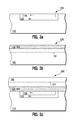
- FIGS. 1-3 show a semiconductor structure, in accordance with first embodiments of the present of invention.
- FIGS. 4-6 show another semiconductor structure in accordance with second embodiments of the present invention.
- FIG. 1 shows a cross-section view of a semiconductor structure 100 , in accordance with embodiments of the present of invention. More specifically, in one embodiment, the semiconductor structure 100 comprises a P ⁇ semiconductor substrate 110 and an insulating layer 130 , e.g. a buried oxide (BOX) layer, on the P ⁇ semiconductor (e.g., silicon, germanium, etc.) substrate 110 .
- a P ⁇ semiconductor substrate 110 e.g., silicon, germanium, etc.
- BOX buried oxide
- the semiconductor structure 100 further comprises a device layer 132 on the BOX layer 130 .
- the device layer 132 includes many device regions 131 (comprising silicon in one embodiment) but only three device regions 131 are shown in FIG. 1 . It should be noted that the device layer 132 may include active devices such as transistors.
- the semiconductor structure 100 further comprises (i) interconnect layers 140 (or also referred to as BEOL layer—Back End Of Line layer) on the device layer 132 and (ii) shallow trench isolation (STI) regions 144 for electrically separating the device regions 131 from each other.
- the STI regions 144 comprise silicon dioxide.
- the semiconductor structure 100 further comprises (i) N+ doped silicon regions 141 b and 142 b in the P ⁇ semiconductor substrate 110 and (ii) diode contact regions 141 and 142 in direct physical contact with the N+ doped silicon regions 141 b and 142 b , respectively.
- the diode contact regions 141 and 142 comprise N+ doped polysilicon.
- the N+ doped silicon region 141 b and the P ⁇ semiconductor substrate 110 form a first P ⁇ N junction.
- the first P ⁇ N junction can be considered a P ⁇ N junction diode which can be referred to as a P ⁇ N junction diode 141 b + 110 .
- the N+ doped silicon region 142 b and the P ⁇ semiconductor substrate 110 form a second P ⁇ N junction.
- the second P ⁇ N junction can be considered a P ⁇ N junction diode which can be referred to as a P ⁇ N junction diode 142 b + 110 .
- the semiconductor structure 100 further comprises a substrate contact region 143 in direct physical contact with the P ⁇ semiconductor substrate 110 .
- the substrate contact region 143 comprises polysilicon.
- the BEOL layer 140 may have many wires (not shown) that provide electrical paths to the device regions 131 , the diode contact regions 141 and 142 , and the substrate contact region 143 of the semiconductor structure 100 .
- the formation of the semiconductor structure 100 of FIG. 1 is as follows. Illustratively, the formation of the semiconductor structure 100 starts with an SOI (silicon on insulator) substrate 110 + 130 + 132 which comprises the layers 110 , 130 , and 132 .
- SOI silicon on insulator
- the STI regions 144 are formed in the device layer 132 of the SOI substrate 110 + 130 + 132 using a conventional method so as to form the device regions 131 .
- contact holes 141 , 142 , and 143 are formed in the SOI substrate 110 + 130 + 132 using a conventional method. Then, insulating layers 141 a , 142 a , and 143 a are formed on sidewalls of the contact holes 141 , 142 , and 143 , respectively using a conventional method.
- the contact holes 141 and 142 are filled with N+ doped polysilicon having dopants with a high diffusivity in silicon, e.g. phosphorus, so as to form the diode contact regions 141 and 142 , respectively.
- the contact hole 143 is filled with P+ polysilicon so as to form the substrate contact region 143 .
- the semiconductor structure 100 is annealed at high temperatures such that dopants from the diode contact regions 141 and 142 diffuse into the P ⁇ semiconductor substrate 110 resulting in the N+ doped silicon regions 141 b and 142 b , respectively.
- devices such as transistors, capacitors, and resistors are fabricated in the device regions 131 using conventional methods.
- the BEOL layer 140 is formed on top the device layer 132 using a conventional method so as to provide electrical paths to the diode contact regions 141 and 142 , the device regions 131 in the device layer 132 , and the substrate contact region 143 .
- the charge neutralizing operation of the structure 100 is as follows.
- the voltage potential of the P ⁇ semiconductor substrate 110 is set at ⁇ 4V
- the voltage potentials of the N+ doped silicon regions 141 b and 142 b are set at ⁇ 5V.
- the P ⁇ N junction diodes 141 b + 110 and 142 b + 110 are forward biased. Therefore, electrons are injected from the N+ doped silicon regions 141 b and 142 b into the P ⁇ semiconductor substrate 110 .
- the voltage potentials of the device regions 131 are set at values higher than the voltage potential of the P ⁇ semiconductor substrate 110 .
- the injected electrons in the P ⁇ semiconductor substrate 110 are pulled toward the device regions 131 and some of the injected electrons can enter the BOX layer 130 and neutralize trapped holes which may be present in the BOX layer 130 .
- electron-hole pairs may be created in the BOX layer 130 .
- the electrons of the created electron-hole pairs having high mobility can easily escape the BOX layer 130 , whereas the holes of the created electron-hole pairs having low mobility become trapped holes in the BOX layer 130 .
- some standard processing steps involve tools that emit ionizing radiation, such as soft X-rays, so the standard process can generate trapped holes in the BOX layer 130 .
- the voltage potentials of the device regions 131 are set in a range from ground (i.e., 0V) to VDD wherein the VDD is in a range from 0.5V to 5V.
- the P ⁇ semiconductor substrate 110 , the substrate contact region 143 and the diode contact regions 141 and 142 are connected to the ground, whereas the device regions 131 are coupled to voltage potentials in the operating voltage range from 0V to VDD.
- FIG. 2 shows a cross-section view of a structure 200 , in accordance with embodiments of the present invention.
- the structure 200 of FIG. 2 is similar to the structure 100 of FIG. 1 , except that the structure 200 comprises (i) an N+ well 120 in the semiconductor substrate 110 , (ii) a P ⁇ well 150 in the N+ well 120 , (iii) an N+ well contact region 145 electrically coupled to the N+ well 120 , and (iv) a P ⁇ well contact region 146 electrically coupled to the P ⁇ well 150 .
- the contact regions of the structure 200 of FIG. 2 are formed using any conventional method.
- the fabrication of the structure 200 of FIG. 2 is similar to the fabrication of the structure 100 of FIG. 1 , except that the N+ well 120 and P ⁇ well 150 can be formed by ion implantation.
- the formation of the SOI substrate 110 + 130 + 132 for forming the structure 200 of FIG. 2 is as follows. Illustratively, on one hand with reference to FIG. 3A , the formation of the SOI substrate 110 + 130 + 132 is started with the substrate 110 . Next, in one embodiment, the N+ well 120 and the P ⁇ well 150 are respectively formed on the top surface of the substrate 110 by ion implantation resulting in a structure 220 of FIG. 3A (also called handler wafer 220 ).
- the BOX layer 130 is formed on a wafer 230 by, illustratively, a chemical vapor deposition (CVD) process.
- CVD chemical vapor deposition
- hydrogen ions are implanted in the silicon substrate 160 so as to form a hydrogen ion layer 161 embedded in the silicon substrate 160 .
- the portion of the silicon substrate 160 above the hydrogen ion layer 161 will become the device layer 132 .
- the wafer 230 of FIG. 3B is turned upside down and bonded to the handler wafer 220 of FIG. 3A , resulting in the structure 200 of FIG. 3C .
- the structure 200 of FIG. 3C is annealed so that the structure 200 of FIG. 3C splits along the hydrogen ion layer 161 (SMARTCUTTM process).
- the lower portion of the structure 200 of FIG. 3C after the split is the SOI substrate 110 + 130 + 132 which is used to form the structure 200 of FIG. 2 .
- the charge neutralizing operation of the structure 200 is similar to the charge neutralizing operation of the structure 100 of FIG. 1 . More specifically, for illustration, the voltage potential of the P ⁇ well 150 is set at ⁇ 4V, and the voltage potentials of the N+ doped silicon regions 141 b and 142 b are set at ⁇ 5V. In one embodiment, the N+ well 120 and the semiconductor substrate 110 are coupled to ground, and the voltage potentials of the device regions 131 are set in a range from ground to VDD. As a result, electrons are injected from the N+ doped silicon regions 141 b and 142 b into the P ⁇ well 150 . Then, the injected electrons in the P ⁇ well 150 are pulled toward the device regions 131 and some of the injected electrons may enter the BOX layer 130 and may neutralize trapped holes which may be present in the BOX layer 130 .
- the N+ well 120 and the semiconductor substrate 110 being at ground ensures that devices (not shown) in the device regions 131 not directly above the P ⁇ well 150 can be in normal operation during the charge neutralizing operation described above.
- FIG. 4 shows a cross-section view of a structure 400 , in accordance with embodiments of the present invention.
- the structure 400 is similar to the structure 100 of FIG. 1 , except that the N+ doped silicon regions 141 b and 142 b and the diode contact regions 141 and 142 of FIG. 1 are replaced by (i) an N+ silicon layer 170 and (ii) a diode contact region 171 (comprising polysilicon in one embodiment) electrically coupled to the N+ silicon layer 170 , respectively.
- the N+ silicon layer 170 is sandwiched between the P ⁇ semiconductor substrate 110 and the BOX layer 130 .
- the formation of the structure 400 of FIG. 4 is similar to the formation of the structure 100 of FIG. 1 , wherein the N+ silicon layer 170 can be formed by ion implantation.
- the formation of the SOI substrate 110 + 170 + 130 + 132 for forming the structure 400 of FIG. 4 is as follows. Illustratively, on one hand, with reference to FIG. 5A , the formation of the structure 400 ( FIG. 4 ) is started with the P ⁇ semiconductor substrate 110 . Next, in one embodiment, a top layer 170 of P ⁇ semiconductor substrate 110 is heavily doped by, illustratively, ion implantation, with N-type dopants (such as arsenic) to form the N+ silicon layer 170 , resulting in the structure 520 of FIG. 5A (also called a handler wafer 520 ).
- N-type dopants such as arsenic
- a wafer 530 is formed.
- the formation of wafer 530 of FIG. 5B is similar to the formation of wafer 230 of FIG. 3B as described above.
- the wafer 530 of FIG. 5B is turned upside down and bonded to the handler wafer 520 of FIG. 5A , resulting in the structure 400 of FIG. 5C .
- the structure 400 of FIG. 5C is annealed so that the structure 400 of FIG. 5C splits along the hydrogen ion layer 161 .
- the lower portion of the structure 400 of FIG. 5C after the split is the SOI substrate 110 + 170 + 130 + 132 which is used to form the structure 400 of FIG. 4 .
- the charge neutralizing operation of the structure 400 is as follows. More specifically, for illustration, the voltage potential of the P ⁇ semiconductor substrate 110 is set at ⁇ 5V, the voltage potential of the N+ silicon layer 170 is set at ⁇ 1V, and the device layers 131 are set at a voltage higher than the voltage of the N+ silicon layer 170 . In one embodiment, the device layers 131 are set at a voltage in a range from ground to VDD. As a result, the P ⁇ N junction diode 170 + 110 is reverse biased resulting in a depletion layer (not shown) at P ⁇ N junction of the P ⁇ N junction diode 170 + 110 .
- the contact regions 171 and 172 of the structure 400 of FIG. 4 are formed using any conventional method.
- the structure 400 of FIG. 4 is exposed to radiation (not shown) to create electron-hole pairs in the depletion layer of the P ⁇ N junction diode 170 + 110 .
- the structure 400 of FIG. 4 is put on a heat chuck (not shown) to create electron-hole pairs in the depletion layer of the P ⁇ N junction diode 170 + 110 through thermal generation. The electrons of the created electron-hole pairs in the depletion layer are accelerated up by the electric field and move in the direction from the P ⁇ semiconductor substrate 110 to the N+ silicon layer 170 .
- a thickness 175 of the N+ silicon layer 170 is such that some of the accelerated electrons pass through the N+ silicon layer 170 and enter the BOX layer 130 and neutralize trapped holes that may be present there.
- the P ⁇ semiconductor substrate 110 , the substrate contact region 172 , and the diode contact region 171 are connected to the ground, whereas the device regions 131 are coupled to voltage potentials in the operating voltage range from 0V to VDD.
- FIG. 6 shows a cross-section view of a structure 600 , in accordance with embodiments of the present invention.
- the structure 600 of FIG. 6 is similar to the structure 400 of FIG. 4 , except that the structure 600 comprises (i) an N+ well 120 in the semiconductor substrate 110 , (ii) a P ⁇ well 150 in the N+ well 120 , (iii) an N+ well contact region 173 electrically coupled to the N+ well 120 , and (iv) a P ⁇ well contact region 172 electrically coupled to the P ⁇ well 150 .
- the fabrication of the structure 600 of FIG. 6 is similar to the fabrication of the structure 400 of FIG. 4 , wherein the N+ well 120 and P ⁇ well 150 can be formed by ion implantation. In one embodiment, the contact regions of the structure 600 of FIG. 6 are formed using any conventional method.
- the charge neutralizing operation of the structure 600 is similar to the charge neutralizing operation of the structure 400 of FIG. 4 . More specifically, for illustration, the voltage potential of the P ⁇ well 150 is set at ⁇ 5V, and the voltage potential of the N+ silicon layer 170 is set at ⁇ 1V. In one embodiment, the N+ well 120 and the semiconductor substrate 110 are coupled to ground, and the voltage potentials of the device regions 131 are set at a voltage higher than the voltage of the N+ silicon layer 170 . In one embodiment, the device layers 131 are set at a voltage in a range from ground to VDD.
- the structure 600 of FIG. 6 is exposed to radiation (not shown) to create electron-hole pairs in the depletion layer of the P ⁇ N junction diode 170 + 110 .
- the structure 600 of FIG. 6 is put on a heat chuck (not shown) to create electron-hole pairs in the depletion layer of the P ⁇ N junction diode 170 + 110 through thermal generation. The electrons of the created electron-hole pairs in the depletion layer are accelerated up by the electric field and move in the direction from the P ⁇ semiconductor substrate 110 to the N+ silicon layer 170 .
- a thickness 176 of the N+ silicon layer 170 is such that some of the accelerated electrons pass through the N+ silicon layer 170 and enter the BOX layer 130 and neutralize trapped holes that may be present there. It should be noted that the N+ well 120 and the semiconductor substrate 110 being at ground ensures that devices (not shown) in the device regions 131 not directly above the P ⁇ well 150 can be in normal operation during the charge neutralizing operation described above.
- the charge neutralizing operation of the structures 100 , 200 , 400 , and 600 can be performed in three modes: (i) one time operation mode in which the charge neutralizing operation is performed only when trapped holes are accumulated in the BOX layer 130 exceeding a certain level, (ii) periodic operation mode in which the charge neutralizing operation is performed periodically applicable to the case when the structures 100 , 200 , 400 , 600 are subject to radiation, and (iii) continuous operation mode in which the charge neutralizing operation is performed continuously and simultaneously with the normal operation of the structure 100 , 200 , 400 , 600 .
- the charge neutralization operation can be applied after a charge accumulation monitor circuit indicates the trapped charge in the BOX layer 130 exceeds a preset limit. Note that in case (iii), device design must be done such that devices in the device regions 131 can operate with the potential in the layers below the BOX layer 130 at a potential other than ground.
- the devices directly above the P ⁇ well 150 of the structure 200 of FIG. 2 and the structure 600 of FIG. 6 can be in charge neutralizing operation, while other devices outside the P ⁇ well 150 of the structure 200 and the structure 600 can be in normal operation.
- electrons can be injected into any layer to neutralize the trapped holes there.
- holes can be injected into a layer to neutralize trapped negative charges there using similar methods described above.
- To inject holes into a layer requires reversing dopant polarities and voltage polarities from embodiments to inject electrons into a layer. This would be desirable, e.g., in an insulator which traps electrons instead of holes.
Abstract
Description
Claims (16)
Priority Applications (1)
| Application Number | Priority Date | Filing Date | Title |
|---|---|---|---|
| US12/792,837 US8035200B2 (en) | 2006-02-21 | 2010-06-03 | Neutralization of trapped charge in a charge accumulation layer of a semiconductor structure |
Applications Claiming Priority (2)
| Application Number | Priority Date | Filing Date | Title |
|---|---|---|---|
| US11/276,248 US7736915B2 (en) | 2006-02-21 | 2006-02-21 | Method for neutralizing trapped charge in a charge accumulation layer of a semiconductor structure |
| US12/792,837 US8035200B2 (en) | 2006-02-21 | 2010-06-03 | Neutralization of trapped charge in a charge accumulation layer of a semiconductor structure |
Related Parent Applications (1)
| Application Number | Title | Priority Date | Filing Date |
|---|---|---|---|
| US11/276,248 Division US7736915B2 (en) | 2006-02-21 | 2006-02-21 | Method for neutralizing trapped charge in a charge accumulation layer of a semiconductor structure |
Publications (2)
| Publication Number | Publication Date |
|---|---|
| US20100237475A1 US20100237475A1 (en) | 2010-09-23 |
| US8035200B2 true US8035200B2 (en) | 2011-10-11 |
Family
ID=38428150
Family Applications (2)
| Application Number | Title | Priority Date | Filing Date |
|---|---|---|---|
| US11/276,248 Expired - Fee Related US7736915B2 (en) | 2006-02-21 | 2006-02-21 | Method for neutralizing trapped charge in a charge accumulation layer of a semiconductor structure |
| US12/792,837 Expired - Fee Related US8035200B2 (en) | 2006-02-21 | 2010-06-03 | Neutralization of trapped charge in a charge accumulation layer of a semiconductor structure |
Family Applications Before (1)
| Application Number | Title | Priority Date | Filing Date |
|---|---|---|---|
| US11/276,248 Expired - Fee Related US7736915B2 (en) | 2006-02-21 | 2006-02-21 | Method for neutralizing trapped charge in a charge accumulation layer of a semiconductor structure |
Country Status (1)
| Country | Link |
|---|---|
| US (2) | US7736915B2 (en) |
Citations (9)
| Publication number | Priority date | Publication date | Assignee | Title |
|---|---|---|---|---|
| JPH05136259A (en) | 1991-11-12 | 1993-06-01 | Hitachi Ltd | Semiconductor substrate and semiconductor device |
| US5360752A (en) | 1993-10-28 | 1994-11-01 | Loral Federal Systems Company | Method to radiation harden the buried oxide in silicon-on-insulator structures |
| US5795813A (en) | 1996-05-31 | 1998-08-18 | The United States Of America As Represented By The Secretary Of The Navy | Radiation-hardening of SOI by ion implantation into the buried oxide layer |
| US5923067A (en) | 1997-04-04 | 1999-07-13 | International Business Machines Corporation | 3-D CMOS-on-SOI ESD structure and method |
| US6268630B1 (en) | 1999-03-16 | 2001-07-31 | Sandia Corporation | Silicon-on-insulator field effect transistor with improved body ties for rad-hard applications |
| US6459125B2 (en) | 1998-02-26 | 2002-10-01 | Mitsubishi Denki Kabushiki Kaisha | SOI based transistor inside an insulation layer with conductive bump on the insulation layer |
| US6917078B2 (en) | 2002-08-30 | 2005-07-12 | Micron Technology Inc. | One transistor SOI non-volatile random access memory cell |
| US20050179093A1 (en) | 2004-02-17 | 2005-08-18 | Silicon Space Technology Corporation | Buried guard ring and radiation hardened isolation structures and fabrication methods |
| US7271608B1 (en) | 2002-11-25 | 2007-09-18 | Ridgetop Group, Inc. | Prognostic cell for predicting failure of integrated circuits |
-
2006
- 2006-02-21 US US11/276,248 patent/US7736915B2/en not_active Expired - Fee Related
-
2010
- 2010-06-03 US US12/792,837 patent/US8035200B2/en not_active Expired - Fee Related
Patent Citations (9)
| Publication number | Priority date | Publication date | Assignee | Title |
|---|---|---|---|---|
| JPH05136259A (en) | 1991-11-12 | 1993-06-01 | Hitachi Ltd | Semiconductor substrate and semiconductor device |
| US5360752A (en) | 1993-10-28 | 1994-11-01 | Loral Federal Systems Company | Method to radiation harden the buried oxide in silicon-on-insulator structures |
| US5795813A (en) | 1996-05-31 | 1998-08-18 | The United States Of America As Represented By The Secretary Of The Navy | Radiation-hardening of SOI by ion implantation into the buried oxide layer |
| US5923067A (en) | 1997-04-04 | 1999-07-13 | International Business Machines Corporation | 3-D CMOS-on-SOI ESD structure and method |
| US6459125B2 (en) | 1998-02-26 | 2002-10-01 | Mitsubishi Denki Kabushiki Kaisha | SOI based transistor inside an insulation layer with conductive bump on the insulation layer |
| US6268630B1 (en) | 1999-03-16 | 2001-07-31 | Sandia Corporation | Silicon-on-insulator field effect transistor with improved body ties for rad-hard applications |
| US6917078B2 (en) | 2002-08-30 | 2005-07-12 | Micron Technology Inc. | One transistor SOI non-volatile random access memory cell |
| US7271608B1 (en) | 2002-11-25 | 2007-09-18 | Ridgetop Group, Inc. | Prognostic cell for predicting failure of integrated circuits |
| US20050179093A1 (en) | 2004-02-17 | 2005-08-18 | Silicon Space Technology Corporation | Buried guard ring and radiation hardened isolation structures and fabrication methods |
Non-Patent Citations (2)
| Title |
|---|
| Notice of Allowance (Mail Date Feb. 4, 2010) for U.S. Appl. No. 11/276,248, filed Feb. 21, 2006; Confirmation No. 2838. |
| Nowlin, R.N.; Schrimpf, R.D.; Enlow, E.W.; Combs, W.E.; Pease, R.L.; Mechanism of Ionizing-Radiation-Induced Degradation in Modern Bipolar Devices; IEEE 1991 Bipolar Circuits and Technology Meeting, Sep. 9-10, 1991. pp. 174-177. |
Also Published As
| Publication number | Publication date |
|---|---|
| US7736915B2 (en) | 2010-06-15 |
| US20070195841A1 (en) | 2007-08-23 |
| US20100237475A1 (en) | 2010-09-23 |
Similar Documents
| Publication | Publication Date | Title |
|---|---|---|
| US7566600B2 (en) | SOI device with reduced drain induced barrier lowering | |
| US6798021B2 (en) | Transistor having a graded active layer and an SOI based capacitor | |
| US6268629B1 (en) | Field effect transistor with reduced narrow channel effect | |
| US9853086B2 (en) | CMOS-based thermopile with reduced thermal conductance | |
| US20150364582A1 (en) | Semiconductor device | |
| US7064414B2 (en) | Heater for annealing trapped charge in a semiconductor device | |
| JP2015159180A (en) | semiconductor device | |
| CN101211978A (en) | Semiconductor device | |
| US8183606B2 (en) | Semiconductor device and method of manufacturing the same | |
| CN103022131A (en) | Semiconductor device | |
| TWI668731B (en) | Semiconductor device structures with multiple nitrided layers and methods of forming the same | |
| US20090152670A1 (en) | Semiconductor device and method of fabricating the same | |
| US9231025B2 (en) | CMOS-based thermoelectric device with reduced electrical resistance | |
| US20140008724A1 (en) | Apparatus and Method for MOS Transistor | |
| US7875509B2 (en) | Manufacturing method of semiconductor apparatus and semiconductor apparatus, power converter using the same | |
| US8035200B2 (en) | Neutralization of trapped charge in a charge accumulation layer of a semiconductor structure | |
| US9484203B2 (en) | Methods of manufacturing semiconductor devices | |
| KR100231133B1 (en) | Semiconductor device and method for manufacturing the same | |
| CN109713028B (en) | Semiconductor device and manufacturing method thereof | |
| JP2010232361A (en) | Semiconductor memory device | |
| US6159809A (en) | Method for manufacturing surface channel type P-channel MOS transistor while suppressing P-type impurity penetration | |
| KR100990840B1 (en) | Method for manufacturing semiconductor device provided with three dimensional cylinder surface channel | |
| KR100774818B1 (en) | Silicon on insulator wafer | |
| US20160276389A1 (en) | Solid-state imaging device and manufacturing method thereof | |
| JP2004104142A (en) | Semiconductor device |
Legal Events
| Date | Code | Title | Description |
|---|---|---|---|
| STCF | Information on status: patent grant |
Free format text: PATENTED CASE |
|
| REMI | Maintenance fee reminder mailed | ||
| FPAY | Fee payment |
Year of fee payment: 4 |
|
| SULP | Surcharge for late payment | ||
| AS | Assignment |
Owner name: GLOBALFOUNDRIES U.S. 2 LLC, NEW YORK Free format text: ASSIGNMENT OF ASSIGNORS INTEREST;ASSIGNOR:INTERNATIONAL BUSINESS MACHINES CORPORATION;REEL/FRAME:036550/0001 Effective date: 20150629 |
|
| AS | Assignment |
Owner name: GLOBALFOUNDRIES INC., CAYMAN ISLANDS Free format text: ASSIGNMENT OF ASSIGNORS INTEREST;ASSIGNORS:GLOBALFOUNDRIES U.S. 2 LLC;GLOBALFOUNDRIES U.S. INC.;REEL/FRAME:036779/0001 Effective date: 20150910 |
|
| AS | Assignment |
Owner name: WILMINGTON TRUST, NATIONAL ASSOCIATION, DELAWARE Free format text: SECURITY AGREEMENT;ASSIGNOR:GLOBALFOUNDRIES INC.;REEL/FRAME:049490/0001 Effective date: 20181127 |
|
| FEPP | Fee payment procedure |
Free format text: MAINTENANCE FEE REMINDER MAILED (ORIGINAL EVENT CODE: REM.); ENTITY STATUS OF PATENT OWNER: LARGE ENTITY |
|
| LAPS | Lapse for failure to pay maintenance fees |
Free format text: PATENT EXPIRED FOR FAILURE TO PAY MAINTENANCE FEES (ORIGINAL EVENT CODE: EXP.); ENTITY STATUS OF PATENT OWNER: LARGE ENTITY |
|
| STCH | Information on status: patent discontinuation |
Free format text: PATENT EXPIRED DUE TO NONPAYMENT OF MAINTENANCE FEES UNDER 37 CFR 1.362 |
|
| FP | Expired due to failure to pay maintenance fee |
Effective date: 20191011 |
|
| AS | Assignment |
Owner name: GLOBALFOUNDRIES INC., CAYMAN ISLANDS Free format text: RELEASE BY SECURED PARTY;ASSIGNOR:WILMINGTON TRUST, NATIONAL ASSOCIATION;REEL/FRAME:054636/0001 Effective date: 20201117 |
|
| AS | Assignment |
Owner name: GLOBALFOUNDRIES U.S. INC., NEW YORK Free format text: RELEASE BY SECURED PARTY;ASSIGNOR:WILMINGTON TRUST, NATIONAL ASSOCIATION;REEL/FRAME:056987/0001 Effective date: 20201117 |