US8022748B2 - Power source circuits for driving liquid crystal displays - Google Patents
Power source circuits for driving liquid crystal displays Download PDFInfo
- Publication number
- US8022748B2 US8022748B2 US12/152,203 US15220308A US8022748B2 US 8022748 B2 US8022748 B2 US 8022748B2 US 15220308 A US15220308 A US 15220308A US 8022748 B2 US8022748 B2 US 8022748B2
- Authority
- US
- United States
- Prior art keywords
- voltage
- circuit
- high voltage
- resistor
- transistor
- Prior art date
- Legal status (The legal status is an assumption and is not a legal conclusion. Google has not performed a legal analysis and makes no representation as to the accuracy of the status listed.)
- Active, expires
Links
Images


Classifications
-
- G—PHYSICS
- G09—EDUCATION; CRYPTOGRAPHY; DISPLAY; ADVERTISING; SEALS
- G09G—ARRANGEMENTS OR CIRCUITS FOR CONTROL OF INDICATING DEVICES USING STATIC MEANS TO PRESENT VARIABLE INFORMATION
- G09G3/00—Control arrangements or circuits, of interest only in connection with visual indicators other than cathode-ray tubes
- G09G3/20—Control arrangements or circuits, of interest only in connection with visual indicators other than cathode-ray tubes for presentation of an assembly of a number of characters, e.g. a page, by composing the assembly by combination of individual elements arranged in a matrix no fixed position being assigned to or needed to be assigned to the individual characters or partial characters
- G09G3/34—Control arrangements or circuits, of interest only in connection with visual indicators other than cathode-ray tubes for presentation of an assembly of a number of characters, e.g. a page, by composing the assembly by combination of individual elements arranged in a matrix no fixed position being assigned to or needed to be assigned to the individual characters or partial characters by control of light from an independent source
- G09G3/36—Control arrangements or circuits, of interest only in connection with visual indicators other than cathode-ray tubes for presentation of an assembly of a number of characters, e.g. a page, by composing the assembly by combination of individual elements arranged in a matrix no fixed position being assigned to or needed to be assigned to the individual characters or partial characters by control of light from an independent source using liquid crystals
- G09G3/3611—Control of matrices with row and column drivers
- G09G3/3696—Generation of voltages supplied to electrode drivers
-
- G—PHYSICS
- G09—EDUCATION; CRYPTOGRAPHY; DISPLAY; ADVERTISING; SEALS
- G09G—ARRANGEMENTS OR CIRCUITS FOR CONTROL OF INDICATING DEVICES USING STATIC MEANS TO PRESENT VARIABLE INFORMATION
- G09G2300/00—Aspects of the constitution of display devices
- G09G2300/06—Passive matrix structure, i.e. with direct application of both column and row voltages to the light emitting or modulating elements, other than LCD or OLED
-
- G—PHYSICS
- G09—EDUCATION; CRYPTOGRAPHY; DISPLAY; ADVERTISING; SEALS
- G09G—ARRANGEMENTS OR CIRCUITS FOR CONTROL OF INDICATING DEVICES USING STATIC MEANS TO PRESENT VARIABLE INFORMATION
- G09G2330/00—Aspects of power supply; Aspects of display protection and defect management
- G09G2330/02—Details of power systems and of start or stop of display operation
- G09G2330/021—Power management, e.g. power saving
-
- H—ELECTRICITY
- H02—GENERATION; CONVERSION OR DISTRIBUTION OF ELECTRIC POWER
- H02M—APPARATUS FOR CONVERSION BETWEEN AC AND AC, BETWEEN AC AND DC, OR BETWEEN DC AND DC, AND FOR USE WITH MAINS OR SIMILAR POWER SUPPLY SYSTEMS; CONVERSION OF DC OR AC INPUT POWER INTO SURGE OUTPUT POWER; CONTROL OR REGULATION THEREOF
- H02M3/00—Conversion of DC power input into DC power output
- H02M3/02—Conversion of DC power input into DC power output without intermediate conversion into AC
- H02M3/04—Conversion of DC power input into DC power output without intermediate conversion into AC by static converters
- H02M3/06—Conversion of DC power input into DC power output without intermediate conversion into AC by static converters using resistors or capacitors, e.g. potential divider
- H02M3/07—Conversion of DC power input into DC power output without intermediate conversion into AC by static converters using resistors or capacitors, e.g. potential divider using capacitors charged and discharged alternately by semiconductor devices with control electrode, e.g. charge pumps
Definitions
- This invention is related to power supply circuits (or power source circuits), and, in particular, to power supply circuits (or power source circuits) for driving liquid crystal displays.
- Liquid crystal display screens occupy a broad market in the field of portable displays. Consumers are increasingly requiring low power consumption and high resolution in portable visual switches.
- the display quality of liquid crystal screens is related to the power source voltages of their liquid crystal drive units. Therefore, liquid crystal drive units must have low power consumption, and liquid crystal drive voltages should be symmetrical. Additionally, in order to broaden the practical applicability of liquid crystal drive units, there should be a wide range of options in choosing power source voltages.
- Liquid crystal drive units need to provide high drive voltages, so in terms of reliability, stability, and cost, power source circuits that produce high voltages are normally integrated into the liquid crystal drive units.
- Power source circuits include boost circuits that can achieve low electrical consumption levels by using charge pump circuits that boost voltage through the use of charge pumps along with the accompanying control circuits.
- the produced voltage is a whole-number multiple of an externally-provided system voltage (in theory), and an appropriate liquid crystal drive voltage cannot be directly produced.
- a low dropout regulator (LDO) or another structure is further required to regulate the production of stable high voltage for use in driving the liquid crystal.
- This type of chip may contain a voltage higher than the highest liquid crystal drive voltage, thereby leading to a complex circuit structure and high power consumption.
- the production of the highest negative driving voltage is also normally performed by first using a charge pump circuit to produce a highest negative voltage, then using a subtractor to produce a smaller negative voltage for use as the highest negative driving voltage for the liquid crystal.
- the existence in a chip of a negative voltage even greater than the negative liquid crystal driving voltage can also lead to circuit complexity and high energy consumption.
- An object of the present invention is to provide a type of power source circuit having low structure complexity and low power consumption for driving liquid crystal displays.
- Another object of the present invention is to provide a type of liquid crystal drive unit that includes a power source circuit and a liquid crystal drive element.
- this invention provides a type of power source circuit, comprising a charge pump circuit used to operate the charge pump to produce driving voltages; a first control circuit, used in the closed-loop control of said charge pump circuit to produce a positive high voltage; a bias-ratio circuit, used with the positive high voltage and the zero-potential voltage produced by the first control circuit to produce a positive sub-high voltage and a lowest positive high voltage; and a second control circuit, used in accordance with the positive sub-high voltage and the lowest positive high voltage produced by said bias-ratio circuit in the closed-loop control of said charge pump circuit to produce a negative high voltage.
- the system contains no voltage higher than the liquid crystal's driving voltages, and also does not contain any lower negative voltage than the liquid crystal's highest negative driving voltage, thereby reducing the circuit's electrical consumption.
- An advantage of the present invention is that it provides a type of power source circuit having low structure complexity and low power consumption for driving liquid crystal displays.
- Another advantage of the present invention is that it provides a type of liquid crystal drive unit that includes a power source circuit and a liquid crystal drive element.
- FIG. 1 contains a structural diagram of the liquid crystal display unit of the liquid crystal drive unit in the embodiments of this invention.
- FIG. 2 is a waveform diagram of the voltages of the COM and SEG electrodes in the embodiments of this invention.
- FIG. 3 is a diagram of the relationship between the driving voltages of the COM and SEG electrodes in the embodiments of this invention.
- FIG. 4 is a structural diagram of the power source circuit provided by the embodiments of this invention.
- FIG. 5 is a structural diagram of the charge pump circuit provided by the embodiments of this invention.
- FIG. 6 is a waveform diagram of the charge pump circuit's reference time sequences provided by the embodiments of this invention.
- FIG. 7 is a diagram of the relationships between and production sequences of the various stages of the charge pump circuit provided by the embodiments of this invention.
- FIG. 8 is a structural diagram of the first control circuit provided by the embodiments of this invention.
- FIG. 9 is a structural diagram of the bias-ratio circuit provided by the embodiments of this invention.
- FIG. 10 is a structural diagram of the second control circuit provided by the embodiments of this invention.
- FIG. 11 is a technological cross-section drawing of the MOS switches that make up the N channel and P channel provided by the embodiments of this invention.
- control circuit through the control circuit's closed-loop control of the conductivity and non-conductivity of the charge pump circuit's on-off switches, by controlling the charge pump circuit, stable highest positive and highest negative liquid crystal drive voltages are directly produced. This reduces power consumption and leads to a simple, easily realized structure.
- FIG. 1 shows a structure of the liquid crystal display unit of the liquid crystal drive unit in the embodiments of this invention. For convenience of explanation, only portions related to these embodiments are shown.
- the liquid crystal display unit ( 10 ) includes the liquid crystal screen ( 11 ) and the liquid crystal drive unit ( 12 ).
- the liquid crystal screen ( 11 ) includes column electrodes (COM), and row electrodes (SEG).
- COM electrodes are also called public electrodes or scanning electrodes; SEG electrodes are also called segment electrodes or data electrodes.
- the number of COM electrodes and SEG electrodes varies with the size of the liquid crystal screen ( 11 ). Pixels are located at the positions corresponding to the intersection points between correlated COM electrodes and SEG electrodes. Each pixel is formed by sealing liquid crystals between COM electrodes and SEG electrodes, and their transparency varies with the voltage applied to the COM electrodes and SEG electrodes.
- the pixels in the liquid crystal screen ( 11 ) can be divided into selected points, non-selected points, and semi-selected points. Pixels that are selected in both the row and column directions are selected points; pixels that are selected in neither the row nor column directions are non-selected points; and pixels that are selected in one of either the row or column directions are semi-selected points.
- the liquid crystal electrode voltage includes both selected voltage and non-selected voltage.
- the liquid crystal drive unit ( 12 ) contains a power source circuit ( 121 ), an X drive part ( 122 ), and a Y drive part ( 123 ).
- the power source circuit ( 121 ) produces the SEG electrode driving voltage and COM electrode driving voltage in accordance with the externally provided zero-potential voltage (VSS) and the externally provided system power source voltage (VIN).
- the X drive part ( 122 ) drives the liquid crystal screen's ( 11 ) SEG electrodes SEG 1 -SEG N using the SEG driving voltage produced by the power source circuit ( 121 ).
- the Y drive part ( 123 ) drives the liquid crystal screen's ( 11 ) COM electrodes COM 1 -COM M using the COM driving voltage produced by the power source circuit ( 121 ).
- FIG. 2 shows the waveform of the voltages of the COM and SEG electrodes in the embodiments of this invention.
- This embodiment contains five driving voltages: a positive high voltage VH, a positive sub-high voltage VG, a lowest positive high voltage VM, a zero-potential voltage VSS, and a negative high voltage VL.
- the magnitude relationships between these five voltages are as follows: VH>VG>VM>VSS>VL.
- the positive high voltage VH and the negative high voltage VL are the most positive and the most negative liquid crystal driving voltages; the liquid crystal drive system does not contain any higher positive voltage than the highest positive driving voltage used by the liquid crystals, nor does it contain any lower negative voltage than the highest negative driving voltage used by the liquid crystals.
- the resistance-divided voltage between the positive high voltage VH and the zero-potential voltage VSS produces the positive sub-high voltage VG and the lowest positive high voltage VM.
- VH, VL, and VM are the COM electrode voltages; VH and VL are the COM electrode selected voltages. VH is a positive high voltage, VL is a negative high voltage, and both are symmetrical with respect to VM. VM is the COM electrode non-selected voltage. VG and VSS are the SEG electrode voltages, and are also both symmetrical with respect to VM. When the COM electrode selected voltage is VH, the SEG electrode selected voltage is VSS and the non-selected voltage is VG When the COM electrode selected voltage is VL, the SEG electrode selected voltage is VG and the non-selected voltage is VSS.
- FIG. 3 shows the relationship between the driving voltages of the COM and SEG electrodes in the embodiments of this invention.
- VH is a positive high voltage
- VL is a negative high voltage
- both are symmetrical with respect to VM; for example, the voltages between VM and VL and VM and VH are both 16V.
- VG and VSS are also symmetrical with respect to VM; for example the voltages between VM and VG and VM and VSS are both 2V.
- the ratio of selected voltage to non-selected voltage is the bias-ratio; accordingly, in this invention VH/VM is the bias-ratio.
- the bias-ratio can be programmably controlled, i.e. VH, VG, VM, and VL are adjustable. At the same time, the consistency and symmetry of voltage conversions is ensured, thus resolving the contradiction between voltage adjustability and voltage consistency.
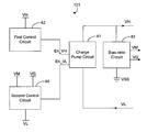
- FIG. 4 shows the structure of the power source circuit provided by the embodiments of this invention, including the charge pump circuit ( 41 ) that produces the liquid crystal driving voltages, and the control circuit and bias-ratio circuit ( 43 ) that through a closed-loop controls the charge pump circuit ( 41 ) to produce the driving voltages.
- the control circuit includes the first control circuit ( 42 ) that controls the charge pump circuit ( 41 ) through a closed-loop to produce a positive high voltage, and the second control circuit ( 44 ) that controls the charge pump ( 41 ) through a closed-loop to produce a negative high voltage.
- VH and VL are directly produced when the first control circuit ( 42 ) and the second control circuit ( 44 ) control the charge pump circuit ( 41 ).
- VG and VM are produced when VH and VSS pass through the bias-ratio circuit ( 43 ) resistance-divided voltage.
- the charge pump circuit ( 41 ) controls the charging and discharging of the capacitor, gradually storing the capacitor's charge in another capacitor, thus boosting its voltage and producing high voltage.
- MOS metal oxide semiconductor
- MOS switches used as examples to demonstrate the realization of the charge pump circuit.
- other on-off switches can be used to realize the charge pump circuit.
- MOS transistors either P-channel MOS transistors or N-channel MOS transistors can be used based on the circuit requirements and according to the circuit principles demonstrated in these embodiments; these embodiments do not represent restrictions on possible circuits.
- the charge pump circuit ( 41 ) can be split into an N-stage (N ⁇ 2) sub-circuit in which each sub-circuit stage has the same circuit structure, and each sub-circuit stage has the same structural principle.
- N ⁇ 1 the first through the (N ⁇ 1)th sub-circuit stages produce the positive high voltage VH
- the Nth sub-circuit stage produces the negative high voltage VL.
- Each sub-circuit stage includes four MOS transistors that serve as on-off switches, one charging and discharging flying capacitor that is used to transfer charge, and one storage capacitor that is used to store charge and stabilize voltage.
- the first and third MOS transistors are serially connected, and the second and fourth MOS transistors are also serially connected.
- One terminal (not serially connected) of the first and fourth MOS transistors receives the kth voltage; one terminal (not serially connected) of the second MOS transistor receives the zero-potential voltage VSS; one terminal (not serially connected) of the third MOS transistor is the voltage output terminal for the kth sub-circuit stage, and connects to one terminal of the storage capacitor and the first MOS transistor of the (k+1)th sub-circuit stage; the other terminal of the storage capacitor receives zero-potential voltage VSS.
- the first and second terminals of the flying capacitor connect to the serially connected terminals of the first and third MOS transistors and the serially connected terminals of the second and fourth MOS transistors, respectively.
- Each sub-circuit stage operates in two time stages.
- the first and second MOS transistors are conductive, and the third and fourth MOS transistors are non-conductive; the kth voltage (e.g. the first sub-circuit stage is the initial voltage) charges the flying capacitor, and the voltage at the flying capacitor's first terminal is higher than the voltage at its second terminal.
- the second stage (T 2 ) the third and fourth MOS transistors are conductive, and the first and second MOS transistors are non-conductive; the voltage at the flying capacitor's second terminal is increased, and because of the capacitor's transient maintenance property, the voltage at the flying capacitor's first terminal is also increased, and the charge is transferred from the flying capacitor to the storage capacitor.
- the first and second time stages are repeated for a sufficient amount of time, after which the storage capacitor's voltage is increased and stabilizes at a specific level, thereby achieving stable high voltage.
- FIG. 5 shows the structure of the charge pump circuit provided by the embodiments of this invention, including 4 sub-circuit stages, all with nearly identical structures and identical operating principles.
- the first control circuit ( 42 ) is the clock signal enabling terminal for the first through the third sub-circuit stages, and controls the production of positive high voltage VH;
- the second control circuit is the clock signal enabling terminal for the fourth sub-circuit stage, and controls the production of negative high voltage VL.
- the first sub-circuit stage is used below as an illustration of the sub-circuit's specific connective structure; the other sub-circuits are similar, and are not described further.
- the first, third, and fourth MOS transistors are P-channel MOS transistors (startup voltage less than zero), while the second MOS transistors is an N-channel MOS transistor (startup voltage greater than zero).
- the first MOS transistor (P 1 ) and the third MOS transistor (P 2 ) are serially connected, and the second MOS transistor (N 1 ) and fourth MOS transistor (P 3 ) are also serially connected.
- the serially connected terminals of the first and third MOS transistors (P 1 , P 2 ) connect to the first terminal of the flying capacitor (C 1 ); the serially connected terminals of the second and fourth MOS transistors (N 1 , P 3 ) are connected to the second terminal of the flying capacitor (C 1 ).
- the first MOS transistor's (P 1 ) drain connects to the third MOS transistor's (P 2 ) source, its gate receives the clock signal CLK 1 , and its source receives externally provided system power source voltage VIN.
- the second MOS transistor's (N 1 ) drain connects to the fourth MOS transistor's (P 3 ) source, its gate receives clock signal CLK 1 N, and its source receives the zero-potential voltage VSS.
- the third MOS transistor's (P 2 ) gate receives clock signal CLK 2 , its drain connects to the first terminal of the second sub-circuit stage's storage capacitor (C 5 ) and the source of the second sub-circuit stage's first MOS transistor (P 5 ), and its storage capacitor's (C 5 ) second terminal receives zero-potential voltage VSS.
- the fourth MOS transistor's (P 3 ) gate receives clock signal CLK 2 , and its drain receives externally provided system power source voltage VIN.
- FIG. 6 shows the waveform of the charge pump circuit's reference time sequence provided by the embodiments of this invention.
- CLK 1 and CLK 2 are non-overlapping clocks; the clocks' non-overlapping time (t) is greater than zero.
- CLK 1 N and CLK 2 N are the reverse clocks of CLK 1 and CLK 2 , respectively.
- the voltage ranges of CLK 1 , CLK 2 , CLK 1 N, and CLK 2 N are all from the system's zero-potential voltage VSS to initial voltage VIN, and all are correspondingly separated into a first stage (T 1 ) and a second stage (T 2 ), wherein the first stage (T 1 ) and second stage (T 2 ) continually alternate back and forth.
- the time sequence of every sub-circuit stage of the charge pump circuit ( 41 ) is produced from the reference time sequence.
- the voltage range of the reference time sequence is from the system's zero-potential voltage VSS to initial voltage VIN, and thus a level shifter must be used to convert the reference voltage to the conductive and non-conductive voltage required by the MOS switches in each sub-circuit stage of the charge pump circuit ( 41 ).
- the first and second MOS transistors (P 1 , N 1 ) are conductive, while the third and fourth (P 2 , P 3 ) are non-conductive.
- Initial voltage VIN charges the flying capacitor (C 1 ), and the voltage at the first terminal of the flying capacitor (C 1 ) is higher than the voltage at the second terminal.
- the third and fourth MOS transistors (P 2 , P 3 ) are conductive, while the first and second MOS transistors (P 1 , N 1 ) are non-conductive.
- the flying capacitor (C 1 ) is serially connected to the storage capacitor (C 5 ), and charge is redistributed. Because initial voltage VIN increases the voltage at the flying capacitor's (C 1 ) second terminal, the flying capacitor (C 1 ) will discharge into the storage capacitor (C 5 ); after this process has been repeated for a sufficient amount of time, the voltage in the storage capacitor (C 5 ) stabilizes at a level of VIN*2 (under ideal conditions with no load consumption), and thus second voltage V 2 X, which is higher than initial voltage VIN, is obtained.
- the negative high voltage VL is obtained through the fourth sub-circuit stage.
- MOS switches P 12 and N 4 are conductive, N 5 and N 6 are non-conductive, the positive high voltage VH charges the flying capacitor C 4 , and the voltage at the first terminal of flying capacitor C 4 is higher than the voltage at the second terminal.
- MOS switches N 5 and N 6 are conductive, and P 12 and N 4 are non-conductive; at this time, flying capacitor C 4 is serially connected to storage capacitor C 8 , and charge is redistributed.
- VSS decreases the voltage at the first terminal of flying capacitor C 4
- the voltage at the first terminal of storage capacitor C 8 is also decreased and the charges of flying capacitor C 4 and storage capacitor C 8 are redistributed. Once this process has been repeated for a sufficient amount of time, the voltage in storage capacitor C 8 stabilizes at the level of positive high voltage VH (under ideal conditions with no load consumption).
- FIG. 8 shows the structure of the first control circuit provided by the embodiments of this invention, including the resistance voltage division circuit ( 81 ) between positive high voltage VH and the zero-potential voltage VSS, the reference voltage production circuit ( 82 ), the error-ratio gauge ( 83 ) and the D trigger sampling circuit ( 84 ).
- the resistance voltage division circuit ( 81 ) produces divided voltage Vr through the resistance-divided voltage between positive high voltage VH and the zero-potential voltage VSS; the reference voltage production circuit ( 82 ) produces the reference voltage Vref through a bandgap reference circuit, and inputs Vref and Vr into the non-inverting and inverting input terminals of the error-ratio gauge ( 83 ), respectively.
- the error-ratio gauge's ( 83 ) output enabling trigger signal is input into the data terminal of the D trigger sampling circuit ( 84 ), and, after the charge pump circuit ( 41 ) sampling the clock enabling signal, becomes the clock enabling terminal for the first through third sub-circuit stages of the charge pump circuit ( 41 ).
- the D trigger sampling circuit ( 84 ) outputs valid positive high voltage clock enabling signal EN_VH to the clock enabling terminals of the charge pump circuit's ( 41 ) first through third sub-circuit stages.
- the charge pump circuit's ( 41 ) clock starts up and performs charging and discharging, charge is continually added to the storage capacitor, and VH is thus increased.
- the voltage at the error-ratio gauge's ( 83 ) non-inverting terminal is less than the voltage at its inverting terminal, and the enabling trigger signal output by the error-ratio gauge ( 83 ) is low.
- the D trigger sampling circuit ( 84 ) outputs an invalid clock enabling signal, the charge pump circuit shuts down, charging and discharging are not performed, charge is no longer added to the storage capacitor, and the voltage stabilizes at Vref*(R 2 +Rx 2 )/Rx 2 .
- FIG. 9 shows the structure of the bias-ratio circuit provided by the embodiments of this invention.
- resistors R 0 , Rx 1 , and Rx 0 are serially connected between the positive high voltage VH and the zero-potential voltage VSS.
- One terminal of resistor R 0 connects to the positive high voltage (VH) output terminal of the charge pump circuit ( 41 ); the other end connects to Rx 1 , while the other terminal of Rx 1 connects to resistor R 0 , and the other terminal of resistor R 0 receives the zero-potential voltage VSS.
- VG is output at the connected terminal of R 0 and Rx 1
- VM is output at the connected terminal of Rx 1 and Rx 0 .
- VH and VG and VM are symmetrical with respect VM, the resistance of resistors Rx 1 and Rx 0 are equal, and vary identically.
- the bias-ratio can be programmably controlled; through the logic control method used to adjust the resistances of resistors Rx 0 and Rx 1 , bias-ratio VH/VM and voltages VM and VG can also be adjusted.
- FIG. 10 shows the structure of the second control circuit provided by the embodiments of this invention, including the resistance voltage division circuit ( 101 ), the error-ratio gauge ( 102 ), and the D trigger sampling circuit ( 103 ).
- resistors Rx 3 and R 3 are serially connected, the terminal of resistor Rx 3 that is not serially connected connects to the positive sub-high voltage (VG) output terminal of the bias-ratio circuit ( 43 ), the terminal of resistor R 3 that is not serially connected receives the negative high voltage VL, and the connected terminal of resistors Rx 3 and R 3 outputs voltage VMX.
- Voltage VMX and VM are input into the non-inverting and inverting input terminals of the error-ratio gauge ( 102 ), respectively.
- the enabling trigger signal output by the error-ratio gauge ( 102 ) is input into the data terminal of the D trigger sampling circuit ( 103 ), and, after the charge pump circuit ( 41 ) sampling the clock enabling signal, becomes the clock enabling terminal for the fourth sub-circuit stage of the charge pump circuit ( 41 ).
- the voltage VMX produced by voltage splitting by the resistance voltage division circuit ( 101 ) and the voltage VM produced by the bias-ratio circuit ( 43 ) are input into the non-inverting and inverting input terminals of the error-ratio gauge ( 102 ).
- the error-ratio gauge ( 102 ) compares said voltages VMX and VM, the enabling trigger signal that it outputs is input into the data terminal of the D trigger sampling circuit ( 103 ), and after going through sampling by the D trigger sampling circuit ( 103 ) it serves as the sequence enabling signal EN_VL for the charge pump circuit's ( 41 ) negative high voltage production circuit, thereby controlling the conductivity and non-conductivity of this portion of MOS switches, and thus controlling the magnitude of the negative high voltage (VL).
- the voltage at the error-ratio gauge's ( 102 ) non-inverting terminal is greater than the voltage at its inverting terminal, the output enabling trigger signal is high, the D trigger sampling circuit ( 103 ) outputs a valid clock enabling signal that serves as the sequence enabling signal EN_VL for the charge pump circuit's ( 41 ) negative high voltage production circuit, the charge pump circuit's ( 41 ) clock starts up, and charging and discharging are performed.
- the voltage at the error-ratio gauge's ( 102 ) non-inverting terminal is less than the voltage at its inverting terminal, the output enabling signal is low, the D trigger sampling circuit ( 103 ) outputs an invalid clock enabling signal, the charge pump circuit ( 41 ) shuts down, and charging and discharging are not performed.
- VL VM ⁇ [VM*R 3/ Rx 3].
- Rx 3 and Rx 0 are adjusted using the same logic control to ensure the consistency of variations in VL and VH.
- MOS transistors can be created in the semiconductor creation process of FIG. 11 ; both high and low voltage MOS elements can be created.
- MOS transistor N 1 in the charge pump circuit is a low voltage N-channel MOS transistor (LVNMOS)
- MOS transistors N 2 , N 3 , N 4 , and N 5 are high voltage N-channel MOS transistors (HVNMOS- 2 )
- MOS transistor N 6 is a high voltages N-channel MOS transistor (HVNMOS- 1 ).
- MOS transistors P 1 , P 2 , and P 3 are low voltage P-channel MOS transistors (LVPMOS), MOS transistors P 4 , P 5 , P 6 , P 7 , P 8 , P 9 , P 11 , and P 12 are high voltage P-channel MOS transistors (HVPMOS).
- HVPMOS high voltage P-channel MOS transistors
- Other logic circuits can be created using low voltage MOS elements.
- the control circuit controls the length of time of conductivity and non-conductivity of the charge pump circuit's on-off switches, and thus controls the amount of charge transferred to the storage capacitor. In this way stable positive and negative voltage are obtained.
- the control circuit's closed-loop control of the charge pump circuit the highest positive and highest negative liquid crystal driving voltages are directly produced.
- the system does not contain any voltage higher than the liquid crystal driving voltages, nor does it contain any voltage lower than the highest negative liquid crystal drive voltage, thereby reducing power consumption, and leading to a simple, easily realized structure.
- the resistance of the resistors and the logic control in the voltage division circuit in the second control circuit in the embodiments of this invention are exactly equal to those of the bias-ratio circuit. This guarantees consistency between changes in the bias-ratio circuit and changes in the negative voltage, and also guarantees excellent consistency and symmetry in changes in the liquid crystal driving voltage.
- a charge pump circuit used in operating the charge pump to produce driving voltages;
- said driving voltages include a positive high voltage, a positive sub-high voltage, a lowest positive high voltage, a zero-potential voltage, and a negative high voltage.
- Said positive high voltage and said negative high voltage, as well as said positive sub-high voltage and said zero-potential voltage are respectively symmetrical with respect to said lowest positive high voltage;
- a first control circuit used in the closed-loop control of said charge pump circuit to produce said positive high voltage
- bias-ratio circuit used in accordance with the positive high voltage and the zero-potential voltage produced by said first control circuit to produce said positive sub-high voltage and said lowest positive high voltage
- a second control circuit used in accordance with the positive sub-high voltage and lowest positive high voltage produced by said bias-ratio circuit in the closed-loop control of said charge pump circuit to produce said negative high voltage.
- Certain other embodiments of this invention is to provide a type of liquid crystal drive unit that includes a power source circuit and a liquid crystal drive element; said power source circuit produces the liquid crystal driving voltages used by said liquid crystal drive element, and said power source circuit includes:
- Said driving voltages include a positive high voltage, a positive sub-high voltage, a lowest positive high voltage, a zero-potential voltage, and a negative high voltage.
- Said positive high voltage and said negative high voltage, as well as said positive sub-high voltage and the zero-potential voltage are symmetrical with respect to said lowest positive high voltage;
- a first control circuit used in the closed-loop control of said of said charge pump circuit to produce said positive high voltage
- bias-ratio circuit used in accordance with the positive high voltage and the zero-potential voltage produced by said first control circuit to produce said positive sub-high voltage and said lowest positive high voltage
- a second control circuit used in accordance with the positive sub-high voltage and the lowest positive high voltage produced by said bias-ratio circuit in the closed-loop control of said charge pump circuit to produce said negative high voltage.
- Certain other embodiments of this invention is to provide a type of liquid crystal display unit that includes a liquid crystal screen and a liquid crystal drive unit;
- said liquid crystal screen includes multiple COM electrodes and SEG electrodes
- said liquid crystal drive unit is used to create the driving voltages for the COM electrodes and SEG electrodes of said liquid crystal screen;
- said liquid crystal drive unit includes a power source circuit, wherein said power source circuit includes:
- a charge pump circuit used in utilizing the charge pump to create driving voltages for the COM electrodes and SEG electrodes of said liquid crystal screen.
- Said driving voltages include a positive high voltage, a positive sub-high voltage, a lowest positive high voltage, a zero-potential voltage, and a negative high voltage.
- Said positive high voltage and said negative high voltage, as well as said positive sub-high voltage and said zero-potential voltage are separately symmetrical with respect to said lowest positive high voltage;
- a first control circuit used in the closed-loop control of said charge pump circuit to produce said positive high voltage
- bias-ratio circuit used in accordance with the positive high voltage and the zero-potential voltage produced by said first control circuit to produce said positive sub-high voltage and the lowest positive high voltage
- a second control circuit used in accordance with the positive sub-high voltage and the lowest positive high voltage produced by said bias-ratio circuit in the closed-loop control of said charge pump circuit to produce said negative high voltage.
- boost circuit includes:
- a charge pump circuit used in utilizing the charge pump to create positive high voltage
- control circuit used in the closed-loop control of said charge pump circuit to produce high voltage in accordance with an external voltage.
- the control circuit through the control circuit's closed-loop control of the conductivity and non-conductivity of the charge pump circuit's on-off switches, stable highest positive and highest negative liquid crystal drive voltages are directly produced by controlling the charge pump circuit.
- the system does not contain any voltage higher than the liquid crystal drive voltages, nor does it contain any voltage lower than the highest negative liquid crystal drive voltage, thereby reducing power consumption, and leading to a simple, easily realized structure, while also ensuring the consistency and symmetry of the positive and negative voltages.
Landscapes
- Engineering & Computer Science (AREA)
- Chemical & Material Sciences (AREA)
- Crystallography & Structural Chemistry (AREA)
- Physics & Mathematics (AREA)
- Computer Hardware Design (AREA)
- General Physics & Mathematics (AREA)
- Theoretical Computer Science (AREA)
- Dc-Dc Converters (AREA)
- Liquid Crystal Display Device Control (AREA)
- Control Of Indicators Other Than Cathode Ray Tubes (AREA)
Abstract
Description
VH*Rx2/(R2+Rx2)=Vr=Vref;
or in another form: VH=Vref*(R2+Rx2)/Rx2.
VG=VH*(Rx1+Rx0)/(R0+Rx1+Rx0);
VM=VH*Rx0/(R0+Rx1+Rx0);
VH=VM*(R0+Rx1+Rx0)/Rx0=VM+[VM*(R0+Rx1)/Rx0].
VG−VL=VM*(R3+Rx3)/R3;
VL=VM−[VM*R3/Rx3].
Claims (20)
Applications Claiming Priority (3)
| Application Number | Priority Date | Filing Date | Title |
|---|---|---|---|
| CN200710074403 | 2007-05-10 | ||
| CN200710074403.0 | 2007-05-10 | ||
| CN2007100744030A CN101303832B (en) | 2007-05-10 | 2007-05-10 | Power supply circuit, liquid crystal drive device, liquid crystal display device |
Publications (2)
| Publication Number | Publication Date |
|---|---|
| US20080291191A1 US20080291191A1 (en) | 2008-11-27 |
| US8022748B2 true US8022748B2 (en) | 2011-09-20 |
Family
ID=40071966
Family Applications (1)
| Application Number | Title | Priority Date | Filing Date |
|---|---|---|---|
| US12/152,203 Active 2030-05-24 US8022748B2 (en) | 2007-05-10 | 2008-05-12 | Power source circuits for driving liquid crystal displays |
Country Status (2)
| Country | Link |
|---|---|
| US (1) | US8022748B2 (en) |
| CN (1) | CN101303832B (en) |
Cited By (1)
| Publication number | Priority date | Publication date | Assignee | Title |
|---|---|---|---|---|
| US20110084675A1 (en) * | 2009-10-08 | 2011-04-14 | Renesas Electronics Corporation | Booster circuit |
Families Citing this family (16)
| Publication number | Priority date | Publication date | Assignee | Title |
|---|---|---|---|---|
| JP5011182B2 (en) * | 2008-03-24 | 2012-08-29 | ルネサスエレクトロニクス株式会社 | Charge pump circuit |
| KR101056331B1 (en) * | 2009-02-27 | 2011-08-11 | 삼성모바일디스플레이주식회사 | Power supply unit, organic light emitting display device using same and driving method thereof |
| CN103258515B (en) * | 2013-05-13 | 2015-08-05 | 京东方科技集团股份有限公司 | Gate drive voltage feeding mechanism, Supply Method and display device |
| CN103714779A (en) * | 2013-12-19 | 2014-04-09 | 电子科技大学 | Source driving circuit and driving method of AMOLED pixel array |
| CN104883051B (en) * | 2015-05-27 | 2017-08-25 | 中国航天科技集团公司第九研究院第七七一研究所 | Negative pressure charge pump circuit in a kind of multi-mode control configurable complimentary piece |
| CN104967307B (en) * | 2015-06-23 | 2017-12-19 | 北京兆易创新科技股份有限公司 | The clock driving method and system of a kind of charge pump |
| CN107666143B (en) * | 2016-07-27 | 2019-03-22 | 帝奥微电子有限公司 | Negative pressure charge pump circuit |
| CN108242221B (en) * | 2016-12-27 | 2023-10-17 | 无锡中微爱芯电子有限公司 | Low-power consumption high-drive LCD bias driving circuit integrated in MCU |
| CN107967904B (en) * | 2018-01-02 | 2020-07-31 | 上海天马微电子有限公司 | Scanning driving circuit, display panel and display device |
| CN111613042A (en) * | 2020-04-26 | 2020-09-01 | 珠海东之尼电子科技有限公司 | Control method of IO common control circuit, remote controller and storage medium |
| US11522446B2 (en) * | 2020-11-19 | 2022-12-06 | Stmicroelectronics International N.V. | Low input supply and low output impedance charge pump circuit configured for positive and negative voltage generation |
| CN113884742B (en) * | 2021-09-10 | 2024-09-06 | 珠海迈巨微电子有限责任公司 | Current detection device, semiconductor chip, battery management system and power-consuming equipment |
| CN116171470B (en) * | 2021-09-24 | 2025-07-25 | 京东方科技集团股份有限公司 | Voltage supply unit, voltage supply method, display driving module and display device |
| CN114812915B (en) * | 2022-06-24 | 2022-10-18 | 中国空气动力研究与发展中心低速空气动力研究所 | Pressure scanning valve circuit |
| CN115881054B (en) * | 2022-12-27 | 2025-10-03 | 上海贝岭股份有限公司 | Liquid crystal display driving device and electronic equipment |
| CN119724122B (en) * | 2024-12-26 | 2026-01-13 | 深圳飞安瑞科技股份有限公司 | A display driver circuit, module, and electronic device |
Citations (3)
| Publication number | Priority date | Publication date | Assignee | Title |
|---|---|---|---|---|
| US6798274B2 (en) * | 2002-03-27 | 2004-09-28 | Sanyo Electric Co., Ltd. | Booster and imaging device using booster |
| US7253676B2 (en) * | 2003-12-25 | 2007-08-07 | Kabushiki Kaisha Toshiba | Semiconductor device and driving method of semiconductor device |
| US7403062B2 (en) * | 2006-12-19 | 2008-07-22 | Aimtron Technology Corp. | Dual edge modulated charge pumping circuit and method |
Family Cites Families (1)
| Publication number | Priority date | Publication date | Assignee | Title |
|---|---|---|---|---|
| EP0721137B1 (en) * | 1994-07-14 | 2004-01-21 | Seiko Epson Corporation | Power source circuit, liquid crystal display device, and electronic device |
-
2007
- 2007-05-10 CN CN2007100744030A patent/CN101303832B/en not_active Expired - Fee Related
-
2008
- 2008-05-12 US US12/152,203 patent/US8022748B2/en active Active
Patent Citations (3)
| Publication number | Priority date | Publication date | Assignee | Title |
|---|---|---|---|---|
| US6798274B2 (en) * | 2002-03-27 | 2004-09-28 | Sanyo Electric Co., Ltd. | Booster and imaging device using booster |
| US7253676B2 (en) * | 2003-12-25 | 2007-08-07 | Kabushiki Kaisha Toshiba | Semiconductor device and driving method of semiconductor device |
| US7403062B2 (en) * | 2006-12-19 | 2008-07-22 | Aimtron Technology Corp. | Dual edge modulated charge pumping circuit and method |
Cited By (1)
| Publication number | Priority date | Publication date | Assignee | Title |
|---|---|---|---|---|
| US20110084675A1 (en) * | 2009-10-08 | 2011-04-14 | Renesas Electronics Corporation | Booster circuit |
Also Published As
| Publication number | Publication date |
|---|---|
| CN101303832A (en) | 2008-11-12 |
| CN101303832B (en) | 2010-12-22 |
| US20080291191A1 (en) | 2008-11-27 |
Similar Documents
| Publication | Publication Date | Title |
|---|---|---|
| US8022748B2 (en) | Power source circuits for driving liquid crystal displays | |
| US8125432B2 (en) | Common voltage generation circuit employing a charge-pump operation to generate low-potential-side voltage | |
| US9030125B2 (en) | Power circuit having multiple stages of charge pumps | |
| US7336273B2 (en) | Power supply voltage converting circuit, control method thereof, display apparatus, and portable terminal | |
| US9361845B2 (en) | Display device compensating clock signal with temperature | |
| US8102357B2 (en) | Display device | |
| JP3693464B2 (en) | Display panel drive device | |
| US20100039364A1 (en) | Drive voltage generating circuit and liquid crystal display including the same | |
| US8674750B2 (en) | Charge pump, a method for controlling the same, and a display driving system comprising the charge pump | |
| KR20070087520A (en) | Shift register circuit and image display device having the same | |
| US20070040825A1 (en) | Display device | |
| CN114944139B (en) | Multi-level output grid transfer circuit and display device | |
| KR20010014560A (en) | Voltage booster circuit, voltage boosting method, and electronic unit | |
| US20240322678A1 (en) | Charge pump circuit, display driver and display device | |
| JP2010118999A (en) | Semiconductor integrated circuit | |
| JP3841083B2 (en) | Boost circuit, power supply circuit, and liquid crystal drive device | |
| KR20060043317A (en) | Voltage supply circuit, voltage supply method, power circuit, electro-optical devices and electronics | |
| CN1993876B (en) | Apparatus comprising a charge pump and LCD driver comprising such an apparatus | |
| US11837132B2 (en) | Output buffer, data driver, and display device having the same | |
| WO2009084278A1 (en) | Power supply circuit and display device including same | |
| US10152937B2 (en) | Semiconductor device, power supply circuit, and liquid crystal display device | |
| US20040141342A1 (en) | Power source circuit | |
| CN119068841B (en) | Gate drive circuit and display device | |
| US20240106434A1 (en) | Output buffer circuit, charge pump device, display drive device, and display device | |
| WO2000058777A1 (en) | Driving method for liquid crystal device and liquid crystal device and electronic equipment |
Legal Events
| Date | Code | Title | Description |
|---|---|---|---|
| AS | Assignment |
Owner name: BYD COMPANY LIMITED, CHINA Free format text: ASSIGNMENT OF ASSIGNORS INTEREST;ASSIGNORS:ZHAO, CHUNBO;YANG, YUN;FENG, WEI;REEL/FRAME:022445/0504 Effective date: 20071029 |
|
| STCF | Information on status: patent grant |
Free format text: PATENTED CASE |
|
| FPAY | Fee payment |
Year of fee payment: 4 |
|
| MAFP | Maintenance fee payment |
Free format text: PAYMENT OF MAINTENANCE FEE, 8TH YEAR, LARGE ENTITY (ORIGINAL EVENT CODE: M1552); ENTITY STATUS OF PATENT OWNER: LARGE ENTITY Year of fee payment: 8 |
|
| AS | Assignment |
Owner name: BYD MICROELECTRONICS CO., LTD., CHINA Free format text: ASSIGNMENT OF ASSIGNORS INTEREST;ASSIGNOR:BYD COMPANY LIMITED;REEL/FRAME:051561/0906 Effective date: 20200107 |
|
| AS | Assignment |
Owner name: BYD SEMICONDUCTOR COMPANY LIMITED, CHINA Free format text: CHANGE OF NAME;ASSIGNOR:BYD MICROELECTRONICS CO., LTD.;REEL/FRAME:055280/0971 Effective date: 20200121 |
|
| MAFP | Maintenance fee payment |
Free format text: PAYMENT OF MAINTENANCE FEE, 12TH YEAR, LARGE ENTITY (ORIGINAL EVENT CODE: M1553); ENTITY STATUS OF PATENT OWNER: LARGE ENTITY Year of fee payment: 12 |