US8008755B2 - Mold for forming molding member and method of manufacturing LED package using the same - Google Patents
Mold for forming molding member and method of manufacturing LED package using the same Download PDFInfo
- Publication number
- US8008755B2 US8008755B2 US12/076,548 US7654808A US8008755B2 US 8008755 B2 US8008755 B2 US 8008755B2 US 7654808 A US7654808 A US 7654808A US 8008755 B2 US8008755 B2 US 8008755B2
- Authority
- US
- United States
- Prior art keywords
- mold
- package substrate
- projecting portion
- convex portion
- preparing
- Prior art date
- Legal status (The legal status is an assumption and is not a legal conclusion. Google has not performed a legal analysis and makes no representation as to the accuracy of the status listed.)
- Expired - Fee Related, expires
Links
Images


Classifications
-
- B—PERFORMING OPERATIONS; TRANSPORTING
- B29—WORKING OF PLASTICS; WORKING OF SUBSTANCES IN A PLASTIC STATE IN GENERAL
- B29C—SHAPING OR JOINING OF PLASTICS; SHAPING OF MATERIAL IN A PLASTIC STATE, NOT OTHERWISE PROVIDED FOR; AFTER-TREATMENT OF THE SHAPED PRODUCTS, e.g. REPAIRING
- B29C45/00—Injection moulding, i.e. forcing the required volume of moulding material through a nozzle into a closed mould; Apparatus therefor
- B29C45/14—Injection moulding, i.e. forcing the required volume of moulding material through a nozzle into a closed mould; Apparatus therefor incorporating preformed parts or layers, e.g. injection moulding around inserts or for coating articles
- B29C45/14336—Coating a portion of the article, e.g. the edge of the article
- B29C45/14418—Sealing means between mould and article
-
- B—PERFORMING OPERATIONS; TRANSPORTING
- B29—WORKING OF PLASTICS; WORKING OF SUBSTANCES IN A PLASTIC STATE IN GENERAL
- B29C—SHAPING OR JOINING OF PLASTICS; SHAPING OF MATERIAL IN A PLASTIC STATE, NOT OTHERWISE PROVIDED FOR; AFTER-TREATMENT OF THE SHAPED PRODUCTS, e.g. REPAIRING
- B29C45/00—Injection moulding, i.e. forcing the required volume of moulding material through a nozzle into a closed mould; Apparatus therefor
- B29C45/14—Injection moulding, i.e. forcing the required volume of moulding material through a nozzle into a closed mould; Apparatus therefor incorporating preformed parts or layers, e.g. injection moulding around inserts or for coating articles
- B29C45/14639—Injection moulding, i.e. forcing the required volume of moulding material through a nozzle into a closed mould; Apparatus therefor incorporating preformed parts or layers, e.g. injection moulding around inserts or for coating articles for obtaining an insulating effect, e.g. for electrical components
- B29C45/14655—Injection moulding, i.e. forcing the required volume of moulding material through a nozzle into a closed mould; Apparatus therefor incorporating preformed parts or layers, e.g. injection moulding around inserts or for coating articles for obtaining an insulating effect, e.g. for electrical components connected to or mounted on a carrier, e.g. lead frame
-
- B—PERFORMING OPERATIONS; TRANSPORTING
- B29—WORKING OF PLASTICS; WORKING OF SUBSTANCES IN A PLASTIC STATE IN GENERAL
- B29C—SHAPING OR JOINING OF PLASTICS; SHAPING OF MATERIAL IN A PLASTIC STATE, NOT OTHERWISE PROVIDED FOR; AFTER-TREATMENT OF THE SHAPED PRODUCTS, e.g. REPAIRING
- B29C45/00—Injection moulding, i.e. forcing the required volume of moulding material through a nozzle into a closed mould; Apparatus therefor
- B29C45/17—Component parts, details or accessories; Auxiliary operations
- B29C45/26—Moulds
- B29C45/34—Moulds having venting means
-
- B—PERFORMING OPERATIONS; TRANSPORTING
- B29—WORKING OF PLASTICS; WORKING OF SUBSTANCES IN A PLASTIC STATE IN GENERAL
- B29C—SHAPING OR JOINING OF PLASTICS; SHAPING OF MATERIAL IN A PLASTIC STATE, NOT OTHERWISE PROVIDED FOR; AFTER-TREATMENT OF THE SHAPED PRODUCTS, e.g. REPAIRING
- B29C45/00—Injection moulding, i.e. forcing the required volume of moulding material through a nozzle into a closed mould; Apparatus therefor
- B29C45/16—Making multilayered or multicoloured articles
- B29C45/1671—Making multilayered or multicoloured articles with an insert
-
- H—ELECTRICITY
- H01—ELECTRIC ELEMENTS
- H01L—SEMICONDUCTOR DEVICES NOT COVERED BY CLASS H10
- H01L2224/00—Indexing scheme for arrangements for connecting or disconnecting semiconductor or solid-state bodies and methods related thereto as covered by H01L24/00
- H01L2224/01—Means for bonding being attached to, or being formed on, the surface to be connected, e.g. chip-to-package, die-attach, "first-level" interconnects; Manufacturing methods related thereto
- H01L2224/42—Wire connectors; Manufacturing methods related thereto
- H01L2224/44—Structure, shape, material or disposition of the wire connectors prior to the connecting process
- H01L2224/45—Structure, shape, material or disposition of the wire connectors prior to the connecting process of an individual wire connector
- H01L2224/45001—Core members of the connector
- H01L2224/45099—Material
- H01L2224/451—Material with a principal constituent of the material being a metal or a metalloid, e.g. boron (B), silicon (Si), germanium (Ge), arsenic (As), antimony (Sb), tellurium (Te) and polonium (Po), and alloys thereof
- H01L2224/45138—Material with a principal constituent of the material being a metal or a metalloid, e.g. boron (B), silicon (Si), germanium (Ge), arsenic (As), antimony (Sb), tellurium (Te) and polonium (Po), and alloys thereof the principal constituent melting at a temperature of greater than or equal to 950°C and less than 1550°C
- H01L2224/45139—Silver (Ag) as principal constituent
-
- H—ELECTRICITY
- H01—ELECTRIC ELEMENTS
- H01L—SEMICONDUCTOR DEVICES NOT COVERED BY CLASS H10
- H01L2224/00—Indexing scheme for arrangements for connecting or disconnecting semiconductor or solid-state bodies and methods related thereto as covered by H01L24/00
- H01L2224/01—Means for bonding being attached to, or being formed on, the surface to be connected, e.g. chip-to-package, die-attach, "first-level" interconnects; Manufacturing methods related thereto
- H01L2224/42—Wire connectors; Manufacturing methods related thereto
- H01L2224/47—Structure, shape, material or disposition of the wire connectors after the connecting process
- H01L2224/48—Structure, shape, material or disposition of the wire connectors after the connecting process of an individual wire connector
- H01L2224/4805—Shape
- H01L2224/4809—Loop shape
- H01L2224/48091—Arched
-
- H—ELECTRICITY
- H01—ELECTRIC ELEMENTS
- H01L—SEMICONDUCTOR DEVICES NOT COVERED BY CLASS H10
- H01L2224/00—Indexing scheme for arrangements for connecting or disconnecting semiconductor or solid-state bodies and methods related thereto as covered by H01L24/00
- H01L2224/01—Means for bonding being attached to, or being formed on, the surface to be connected, e.g. chip-to-package, die-attach, "first-level" interconnects; Manufacturing methods related thereto
- H01L2224/42—Wire connectors; Manufacturing methods related thereto
- H01L2224/47—Structure, shape, material or disposition of the wire connectors after the connecting process
- H01L2224/48—Structure, shape, material or disposition of the wire connectors after the connecting process of an individual wire connector
- H01L2224/481—Disposition
- H01L2224/48151—Connecting between a semiconductor or solid-state body and an item not being a semiconductor or solid-state body, e.g. chip-to-substrate, chip-to-passive
- H01L2224/48221—Connecting between a semiconductor or solid-state body and an item not being a semiconductor or solid-state body, e.g. chip-to-substrate, chip-to-passive the body and the item being stacked
- H01L2224/48245—Connecting between a semiconductor or solid-state body and an item not being a semiconductor or solid-state body, e.g. chip-to-substrate, chip-to-passive the body and the item being stacked the item being metallic
- H01L2224/48247—Connecting between a semiconductor or solid-state body and an item not being a semiconductor or solid-state body, e.g. chip-to-substrate, chip-to-passive the body and the item being stacked the item being metallic connecting the wire to a bond pad of the item
-
- H—ELECTRICITY
- H01—ELECTRIC ELEMENTS
- H01L—SEMICONDUCTOR DEVICES NOT COVERED BY CLASS H10
- H01L2924/00—Indexing scheme for arrangements or methods for connecting or disconnecting semiconductor or solid-state bodies as covered by H01L24/00
- H01L2924/0001—Technical content checked by a classifier
- H01L2924/00011—Not relevant to the scope of the group, the symbol of which is combined with the symbol of this group
-
- H—ELECTRICITY
- H01—ELECTRIC ELEMENTS
- H01L—SEMICONDUCTOR DEVICES NOT COVERED BY CLASS H10
- H01L2924/00—Indexing scheme for arrangements or methods for connecting or disconnecting semiconductor or solid-state bodies as covered by H01L24/00
- H01L2924/0001—Technical content checked by a classifier
- H01L2924/00014—Technical content checked by a classifier the subject-matter covered by the group, the symbol of which is combined with the symbol of this group, being disclosed without further technical details
-
- H—ELECTRICITY
- H01—ELECTRIC ELEMENTS
- H01L—SEMICONDUCTOR DEVICES NOT COVERED BY CLASS H10
- H01L2924/00—Indexing scheme for arrangements or methods for connecting or disconnecting semiconductor or solid-state bodies as covered by H01L24/00
- H01L2924/013—Alloys
- H01L2924/0132—Binary Alloys
- H01L2924/01322—Eutectic Alloys, i.e. obtained by a liquid transforming into two solid phases
-
- H—ELECTRICITY
- H01—ELECTRIC ELEMENTS
- H01L—SEMICONDUCTOR DEVICES NOT COVERED BY CLASS H10
- H01L2924/00—Indexing scheme for arrangements or methods for connecting or disconnecting semiconductor or solid-state bodies as covered by H01L24/00
- H01L2924/15—Details of package parts other than the semiconductor or other solid state devices to be connected
- H01L2924/181—Encapsulation
-
- H—ELECTRICITY
- H01—ELECTRIC ELEMENTS
- H01L—SEMICONDUCTOR DEVICES NOT COVERED BY CLASS H10
- H01L33/00—Semiconductor devices with at least one potential-jump barrier or surface barrier specially adapted for light emission; Processes or apparatus specially adapted for the manufacture or treatment thereof or of parts thereof; Details thereof
- H01L33/48—Semiconductor devices with at least one potential-jump barrier or surface barrier specially adapted for light emission; Processes or apparatus specially adapted for the manufacture or treatment thereof or of parts thereof; Details thereof characterised by the semiconductor body packages
- H01L33/52—Encapsulations
- H01L33/54—Encapsulations having a particular shape
Definitions
- the present invention relates to a mold for forming a molding member and a method of manufacturing a light emitting diode (LED) package using the same.
- LEDs are semiconductor elements which convert electric energy into light energy, and are composed of compound semiconductor which emits light with a specific wavelength depending on energy bandgap. Further, LEDs are used in various fields such as optical communication and display.
- LEDs are provided in a package type depending on the use purpose and requested shape thereof.
- an LED package is manufactured by the following method. First, an LED chip is mounted on a substrate having an electrode pattern formed thereon or a lead frame, and a terminal of the LED chip is electrically connected to the electrode pattern (or lead). Then, a molding member is formed on the LED chip by using epoxy, silicon, or a combination thereof, and a convex lens is attached to the molding member. Then, the LED package is completed.
- the lens is formed to increase light emission efficiency within a constant orientation angle. Depending on the shape of the lens, the propagating path of light can be differently set.
- FIGS. 1A to 1D are process diagrams briefly showing a conventional method of manufacturing an LED package.
- a package substrate 13 having an LED chip 11 mounted thereon is prepared, and a molding member 16 surrounding the LED chip 11 is formed.
- the package substrate 13 has a lead frame 15 inserted therein, and the LED chip 11 is mounted on the lead frame 15 , exposed through a groove formed on the top surface of the package substrate 13 , through an adhesive.
- an electrode pattern (not shown) of the LED chip 11 is connected to the lead frame 15 through a wiring process, and transparent resin is injected into the groove and is then solidified to form the molding member 16 .
- the LED chip 11 is mounted on the package substrate 13 , and the molding member 16 is formed on the LED chip 16 . Then, as shown in FIG. 1B , an adhesive for attaching a lens is coated on the surface of the molding member 16 .
- a lens 19 which is previously manufactured by casting or the like is bonded on the adhesive 17 , and the adhesive 17 is then cured by a curing process. Accordingly, as shown in FIG. 1D , the lens 19 is fixed on the molding member 16 .
- the lens is formed on the molding member by the process of attaching the lens, a coupling force between the lens and the package substrate is so weak that they can be easily separated from each other. Further, the lens is separately formed. Therefore, the manufacturing process becomes complicated.
- An advantage of the present invention is that it provides a method of manufacturing an LED package, in which a molding member with a convex lens shape is formed on a package substrate by injecting resin into a mold such that the manufacturing process can be simplified.
- the contact surface between the package substrate and the mold is minimized to thereby prevent resin from leaking and bubbles from being generated.
- a method of manufacturing a light emitting diode (LED) package comprises the steps of: preparing a package substrate having an LED chip mounted thereon; preparing a mold which has a convex portion, a plane portion extending outward from the convex portion, and a projecting portion formed on the lower surface of the plane portion, the projecting portion having a sharp end; engaging the mold with the package substrate such that the projecting portion is contacted with the surface of the package substrate; and filling transparent resin into the convex portion.
- a transparent-resin inlet or air discharge port passing through the package substrate may be formed.
- a transparent-resin inlet or air discharge port passing through the convex portion may be formed.
- a transparent-resin inlet and an air discharge port passing through the package substrate may be formed, or a transparent-resin inlet and an air discharge port passing through the convex portion may be formed.
- a method of manufacturing an LED package comprises the steps of: preparing a package substrate having an LED chip mounted thereon; forming a projecting portion which projects from the surface of the package substrate and has an outer surface inclined toward the inside; preparing a mold which has a convex portion and a plane portion extending outward from the convex portion; engaging the mold with the package substrate such that the mold is contacted with the outer surface of the projecting portion; and filling transparent resin into the convex portion.
- a transparent-resin inlet or air discharge port passing through the package substrate may be formed.
- a transparent-resin inlet or air discharge port passing through the convex portion may be formed.
- a transparent-resin inlet and an air discharge port passing through the package substrate may be formed, or a transparent-resin inlet and an air discharge port passing through the convex portion may be formed.
- a mold for forming a molding member on a package substrate having an LED chip mounted thereon comprises a convex portion; a plane portion that extends from the convex portion to form a plane surface; and a projecting portion that projects from the lower surface of the plane portion and of which the end is sharpened.
- the convex portion may have a through-hole passing through the convex portion.
- the convex portion may have first and second through holes.
- the projecting portion may have first and second surfaces, of which at least one is formed of an inclined surface.
- the first surface forms the outer surface of the projecting portion
- the second surface forms the inner surface of the projecting portion, the second surface extending vertically from the plane portion.
- the first surface forms the outer surface of the projecting portion
- the second surface forms the inner surface of the projecting portion, the first surface extending vertically from the plane portion.
- the first and second surfaces may be formed of inclined surfaces of which the ends meet each other.
- a method of manufacturing an LED package comprises the steps of: preparing a package substrate having an LED chip mounted thereon; preparing a mold which has a convex portion and a plane portion; engaging the mold with the package substrate; and filling transparent resin into the convex portion such that a hemispheric molding member is formed on the LED chip.
- Any one of the mold and the package substrate has a projecting portion with a sharp end.
- the preparing of the package substrate may include the step of: forming a projecting portion which projects from the surface of the package substrate and has an outer inclined surface to be contacted with the mold.
- the preparing of the mold may include the step of: forming a projecting portion which projects from the lower surface of the plane portion and has first and second surfaces of which the ends meet each other.
- first and second surfaces may be formed of an inclined surface.
- the first surface forms the outer surface of the projecting portion, and the second surface forms the inner surface of the projecting portion, the second surface extending vertically from the plane portion.
- the first surface forms the outer surface of the projecting portion, and the second surface forms the inner surface of the projecting portion, the first surface extending vertically from the plane portion.
- the first and second surfaces may be formed of inclined surfaces of which the ends meet each other.
- the method may further include the step of separating the mold from the molding member.
- FIGS. 1A to 1D are process diagrams briefly showing a conventional method of manufacturing an LED package
- FIGS. 2A to 2C are process diagrams for explaining a method of manufacturing a package according to an embodiment of the invention.
- FIG. 3 is a diagram showing an example of an LED package substrate according to the invention.
- FIGS. 4A and 4B are diagrams of a mold for forming a molding member according to an embodiment of the invention.
- FIG. 5 is a cross-sectional view of a mold for forming a molding member according to another embodiment of the invention.
- FIGS. 2A to 2C are process diagrams for explaining a method of manufacturing a package according to an embodiment of the invention.
- FIGS. 4A and 4B are diagrams of a mold for forming a molding member according to an embodiment of the invention.
- a cup-shaped LED package substrate 120 is prepared, which has a groove 145 formed therein and at least one lead frame 110 provided on the bottom surface of the groove 145 .
- the inner side wall of the groove 145 may be formed with a reflecting surface which is inclined upward.
- the LED package substrate 120 is composed of a lower substrate 120 a having the lead frame 110 and an upper substrate 120 b having the groove 145 .
- the LED package substrate may be another package substrate with a cup structure for chip mounting.
- an LED chip 130 is mounted on the bottom surface of the groove 145 , and a terminal (not shown) of the LED chip 130 is electrically connected to the lead frame 110 through a wire 127 .
- the terminal may be connected by a flip-chip method.
- the LED chip 130 may include a submount substrate and an LED chip mounted on the top surface of the submount substrate. Further, the LED chip 130 may be fixed to the top surface of the lead frame 110 through an adhesive such as Ag resin or eutectic solder.
- the LED chip 130 includes at least one or more LEDs which generate blue, red, green, and ultraviolet (UV) wavelengths.
- the LED chip 130 may be composed of only a blue LED or blue and red LEDs.
- the LED chip 130 may be composed of another single LED or other LEDs, if they generate blue, red, green, and UV wavelengths.
- transparent liquid resin mixed with phosphor materials is filled in the groove 145 of the package structure having the LED chip 130 mounted thereon, and is then cured to form a phosphor layer 140 .
- the transparent resin may be input into the groove 145 through a dispensing process or the like and is formed of any one of epoxy, silicon, strained silicon, urethane resin, oxetane resin, acrylic resin, polycarbonate, and polyimide.
- the phosphor layer 140 which is formed by mixing resin with phosphor materials, includes phosphor materials which convert a wavelength into any one of yellow, red, and green.
- the phosphor materials can be determined depending on the light emission wavelength of the LED chip 130 .
- phosphor materials which can convert light emitted from the LED chip 130 to implement white light are used.
- the LED chip 130 is composed of a blue LED
- yellow phosphor materials are used as the phosphor materials.
- the phosphor layer 140 is not an essential component, but may be omitted.
- a first through-hole 150 a passing through the package substrate 120 and the lead frame 110 is formed.
- the first through-hole 150 a may be used as a transparent resin inlet or air discharge port. As shown in FIG. 3 , two through-holes 150 may be formed. That is, the first and second through-holes 150 a and 150 b may be formed so as to be used as a transparent resin inlet and an air discharge port, respectively.
- a mold 160 for forming a molding member is engaged with the surface of the package substrate 120 having the first through-hole 150 a provided therein, and the transparent resin 151 is injected into a space between the package substrate 120 and the mold 160 .
- the transparent resin 151 may be injected by an injector such as a dispenser or the like and is formed of any one of epoxy, silicon, strained silicon, urethane resin, oxetane resin, acrylic resin, polycarbonate, and polyimide.
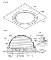
- the mold 160 includes a convex portion 161 , a plane portion 163 extending outward from the convex portion 161 , and a projecting portion 165 formed on the lower surface of the plane portion 164 .
- the projecting portion 165 has an inclined surface.
- the convex portion 161 defines a space between the package substrate 120 and the mold 160 . That is, the space is formed by the convex portion 161 of the mold 160 .
- a second through-hole 150 b is formed in the convex portion 161 of the mold 160 .
- the second through-hole 150 b may be used as a transparent resin inlet or air discharge port.
- the transparent resin is injected into the convex portion 161 through the first through-hole 150 a of the package substrate 120 , the air within the convex portion 161 is discharged to the outside through the second through-hole 150 b provided in the convex portion 161 .
- the transparent resin may be injected through the second through-hole 150 b , and the air may be discharged through the first through-hole 150 a.
- the transparent resin is injected through the first through-hole 150 a , and the air is discharged through the second through-hole 150 b . Therefore, the mold 160 does not need to have a through-hole formed therein.
- the package substrate 120 may not have a through-hole.
- the package structure is moved to a high-temperature chamber to cure the transparent resin.
- the transparent resin 151 filled in the convex portion 161 may leak to the outside such that bubbles are generated in the convex portion 161 .
- the package substrate 120 and the mold 160 are engaged in such a manner that they come in line contact with each other.
- the projecting portion 165 having an inclined surface is provided on the plane portion 163 of the mold 160 contacted with the package substrate 120 .
- the end of the projecting portion 165 is sharpened in such a manner that the contact surface between the package substrate 120 and the mold 160 is minimized.
- the projecting portion 165 is formed to project from the plane portion 163 and has first and second surfaces 165 a and 165 b . At least one of the first and second surfaces 165 a and 165 b is formed of an inclined surface such that the end of the projecting portion 165 has a sharp end.
- both of the first and second surfaces 165 a and 165 b are formed of inclined surfaces, or one of the first and second surfaces 165 a and 165 b is formed of an inclined surface.
- the ends of the first and second surfaces 165 a and 165 b meet each other, the end of the projecting portion 165 has a sharp shape.
- the projecting portion 165 projecting from the plane portion 163 is contacted with the package substrate 120 .
- the projecting portion 165 comes in line contact with the package substrate 120 .
- high pressure may be applied to secure the airtightness within the convex portion 161 .
- the lead frame may be deformed.
- a molding member 152 with a lens shape is formed by separating the mold 160 from the molding member 152 , as shown in FIG. 2C .
- the projecting portion with a sharp end is formed on the surface of the package substrate contacted with the mold such that the contact surface between the package substrate and the mold is minimized. Then, since pressure is concentrated on the end of the projecting portion, it is possible to secure the airtightness of the convex portion without the deformation of the lead frame.
- the transparent resin is prevented from leaking such that bubbles are not generated, it is possible to further enhance light efficiency.
- the projecting portion with a sharp end is formed on the lower surface of the plane portion contacted with the package substrate.
- a projecting portion with a sharp end may be formed on the surface of the package substrate.
- a projecting portion with a sharp end is provided on the surface of the package substrate, which is to be contacted with the mold, such that part of the projecting portion is included in the convex portion. Then, the inclined surface of the projecting portion comes in line contact with the mold.
- FIG. 5 is a cross-sectional view of a mold for forming a molding member according to another embodiment of the invention, showing a state where a projecting portion is formed on the surface of the package substrate such that the package substrate comes in line contact with the mold.
- the package substrate 120 includes a projecting portion 175 formed on the surface thereof, the projecting portion 175 having first and second surfaces 175 a and 175 b of which the ends meet each other.
- At least one of the first and second surfaces 175 a and 175 b is formed of an inclined surface, and the end of the projecting portion 175 has a sharp shape.
- both of the first and second surfaces 175 a and 175 b are formed of inclined surfaces, or only one of the first and second surfaces 175 a and 175 b is formed of an inclined surface.
- the ends of the first and second surfaces 175 a and 175 b meet each other, the end of the projecting portion 175 has a sharp shape.
- the outer surface of the projecting portion 175 that is, the first surface 175 a should be formed of an inclined surface, in order for line contact with the mold 160 .
- the first surface 175 a should be inclined toward the side where the LED chip is mounted.
- part of the projecting portion 175 projecting from the surface of the package substrate 120 is included in the convex portion 161 of the mold 160 , and the first surface 175 a comes in line contact with the mold 160 .
- the mold having the dome-shaped or hemispheric convex portion is prepared and then engaged with the package substrate such that a space is formed in the convex portion. Then, transparent resin is injected into the space and is cured in such a manner that a dome-shaped or hemispheric molding member is formed on the surface of the package substrate.
- the process of attaching a lens to a molding member may be omitted. Therefore, the manufacturing process can be simplified.
- the projecting portion with a sharp end is provided, the contact surface between the mold and the package substrate is minimized when the mold and the package substrate are engaged with each other. Then, the transparent resin is prevented from leaking, so that bubbles are not generated, which makes it possible to enhance light efficiency.
Abstract
Description
Claims (25)
Applications Claiming Priority (2)
| Application Number | Priority Date | Filing Date | Title |
|---|---|---|---|
| KR1020070135476A KR100947400B1 (en) | 2007-12-21 | 2007-12-21 | Mold for forming a molding member and method of fabricating led package using the same |
| KR10-2007-0135476 | 2007-12-21 |
Publications (2)
| Publication Number | Publication Date |
|---|---|
| US20090162957A1 US20090162957A1 (en) | 2009-06-25 |
| US8008755B2 true US8008755B2 (en) | 2011-08-30 |
Family
ID=40789125
Family Applications (1)
| Application Number | Title | Priority Date | Filing Date |
|---|---|---|---|
| US12/076,548 Expired - Fee Related US8008755B2 (en) | 2007-12-21 | 2008-03-19 | Mold for forming molding member and method of manufacturing LED package using the same |
Country Status (2)
| Country | Link |
|---|---|
| US (1) | US8008755B2 (en) |
| KR (1) | KR100947400B1 (en) |
Cited By (1)
| Publication number | Priority date | Publication date | Assignee | Title |
|---|---|---|---|---|
| US20140319562A1 (en) * | 2013-04-29 | 2014-10-30 | Genesis Photonics Inc. | Light-emitting diode package structure |
Families Citing this family (22)
| Publication number | Priority date | Publication date | Assignee | Title |
|---|---|---|---|---|
| KR100761387B1 (en) * | 2005-07-13 | 2007-09-27 | 서울반도체 주식회사 | Mold for forming a molding member and method of fabricating a molding member using the same |
| US20080029774A1 (en) * | 2006-08-04 | 2008-02-07 | Acol Technologies S.A. | Semiconductor light source packages with broadband and angular uniformity support |
| US7915061B2 (en) * | 2007-05-31 | 2011-03-29 | GE Lighting Solutions, LLC | Environmentally robust lighting devices and methods of manufacturing same |
| KR100947400B1 (en) * | 2007-12-21 | 2010-03-12 | 삼성전기주식회사 | Mold for forming a molding member and method of fabricating led package using the same |
| JP5263788B2 (en) * | 2009-10-22 | 2013-08-14 | シャープ株式会社 | Display device |
| JP5263895B2 (en) * | 2010-01-12 | 2013-08-14 | ルネサスエレクトロニクス株式会社 | Semiconductor device and manufacturing method of semiconductor device |
| US8357564B2 (en) * | 2010-05-17 | 2013-01-22 | Stats Chippac, Ltd. | Semiconductor device and method of forming prefabricated multi-die leadframe for electrical interconnect of stacked semiconductor die |
| CN101963296B (en) * | 2010-07-07 | 2013-03-20 | 杨东佐 | Manufacture method of LED integrated structure |
| TW201204986A (en) * | 2010-07-21 | 2012-02-01 | Hon Hai Prec Ind Co Ltd | Light Emitting Diode lead frame assembly and method of making the same |
| DE102011003608A1 (en) * | 2010-08-20 | 2012-02-23 | Tridonic Gmbh & Co. Kg | Housed LED module |
| CN102420282B (en) * | 2010-09-27 | 2014-07-02 | 展晶科技(深圳)有限公司 | Light-emitting diode packaging structure and manufacturing method thereof |
| CN102447042A (en) * | 2010-10-15 | 2012-05-09 | 展晶科技(深圳)有限公司 | LED (Light Emitting Diode) package structure and process |
| KR101761637B1 (en) * | 2010-11-24 | 2017-07-27 | 삼성전자주식회사 | Light emitting diode package and manufaturing method thereof |
| KR20120119350A (en) * | 2011-04-21 | 2012-10-31 | 삼성전자주식회사 | Light emitting device module and method for manufacturing the same |
| KR101289073B1 (en) * | 2011-12-30 | 2013-07-22 | 삼성전자주식회사 | Mold for lighting emitting device package and method of manufacturing lens of light emitting device package |
| US8772819B2 (en) * | 2012-01-19 | 2014-07-08 | GEM Weltronics TWN Corporation | Multi-layer array type LED device |
| US10195928B2 (en) * | 2013-02-08 | 2019-02-05 | Saint-Gobain Glass France | Quarter window assembly for a vehicle door and method of making the assembly |
| CN104157769B (en) * | 2013-05-13 | 2017-04-05 | 新世纪光电股份有限公司 | Package structure for LED |
| CN106058027A (en) * | 2016-06-29 | 2016-10-26 | 深圳市源磊科技有限公司 | LED light source with lens and manufacturing method of LED light source |
| KR102471693B1 (en) | 2017-12-05 | 2022-11-28 | 쑤저우 레킨 세미컨덕터 컴퍼니 리미티드 | Light emitting device package and light source unit |
| WO2019112250A1 (en) * | 2017-12-05 | 2019-06-13 | 엘지이노텍 주식회사 | Light-emitting element package and light source device |
| US10931080B2 (en) | 2018-09-17 | 2021-02-23 | Waymo Llc | Laser package with high precision lens |
Citations (7)
| Publication number | Priority date | Publication date | Assignee | Title |
|---|---|---|---|---|
| US20030168720A1 (en) * | 2002-03-06 | 2003-09-11 | Nichia Corporation | Semiconductor device and manufacturing method for same |
| KR20060135498A (en) | 2005-06-24 | 2006-12-29 | 엘지이노텍 주식회사 | Light emitting device package and mauufacture method of light emitting device package |
| KR20070008269A (en) | 2005-07-13 | 2007-01-17 | 서울반도체 주식회사 | Mold for forming a molding member and method of fabricating a molding member using the same |
| JP2007184310A (en) | 2005-12-29 | 2007-07-19 | Citizen Electronics Co Ltd | Light emitting device |
| US20090162957A1 (en) * | 2007-12-21 | 2009-06-25 | Samsung Electro-Mechanics Co., Ltd. | Mold for forming molding member and method of manufacturing LED package using the same |
| US20100047941A1 (en) * | 2005-06-03 | 2010-02-25 | Samsung Electo-Mechanics Co., Ltd. | High power led package and fabrication method thereof |
| US20100053978A1 (en) * | 2008-08-26 | 2010-03-04 | Han-Ming Lee | Radiating semi-conductor light |
-
2007
- 2007-12-21 KR KR1020070135476A patent/KR100947400B1/en not_active IP Right Cessation
-
2008
- 2008-03-19 US US12/076,548 patent/US8008755B2/en not_active Expired - Fee Related
Patent Citations (8)
| Publication number | Priority date | Publication date | Assignee | Title |
|---|---|---|---|---|
| US20030168720A1 (en) * | 2002-03-06 | 2003-09-11 | Nichia Corporation | Semiconductor device and manufacturing method for same |
| US20100047941A1 (en) * | 2005-06-03 | 2010-02-25 | Samsung Electo-Mechanics Co., Ltd. | High power led package and fabrication method thereof |
| KR20060135498A (en) | 2005-06-24 | 2006-12-29 | 엘지이노텍 주식회사 | Light emitting device package and mauufacture method of light emitting device package |
| KR20070008269A (en) | 2005-07-13 | 2007-01-17 | 서울반도체 주식회사 | Mold for forming a molding member and method of fabricating a molding member using the same |
| US20080268559A1 (en) * | 2005-07-13 | 2008-10-30 | Seoul Semiconductor Co., Ltd. | Mold for Forming a Molding Member and Method of Fabricating a Molding Member Using the Same |
| JP2007184310A (en) | 2005-12-29 | 2007-07-19 | Citizen Electronics Co Ltd | Light emitting device |
| US20090162957A1 (en) * | 2007-12-21 | 2009-06-25 | Samsung Electro-Mechanics Co., Ltd. | Mold for forming molding member and method of manufacturing LED package using the same |
| US20100053978A1 (en) * | 2008-08-26 | 2010-03-04 | Han-Ming Lee | Radiating semi-conductor light |
Non-Patent Citations (1)
| Title |
|---|
| Korean Notice of Allowance dated Dec. 24, 2009 and issued in corresponding Korean Patent Application 10-2007-0135476. |
Cited By (1)
| Publication number | Priority date | Publication date | Assignee | Title |
|---|---|---|---|---|
| US20140319562A1 (en) * | 2013-04-29 | 2014-10-30 | Genesis Photonics Inc. | Light-emitting diode package structure |
Also Published As
| Publication number | Publication date |
|---|---|
| US20090162957A1 (en) | 2009-06-25 |
| KR20090067719A (en) | 2009-06-25 |
| KR100947400B1 (en) | 2010-03-12 |
Similar Documents
| Publication | Publication Date | Title |
|---|---|---|
| US8008755B2 (en) | Mold for forming molding member and method of manufacturing LED package using the same | |
| US10454003B2 (en) | Light emitting device and manufacturing method thereof | |
| US8735190B2 (en) | Batwing LED with remote phosphor configuration | |
| US7452737B2 (en) | Molded lens over LED die | |
| US8188498B2 (en) | Light emitting device package | |
| KR100880638B1 (en) | Light emitting device package | |
| EP1657758B1 (en) | Method of manufacturing a light emitting diode with molded lens | |
| TWI473291B (en) | Light emitting diode component | |
| US9018663B2 (en) | Lens-equipped optical semiconductor device and method for manufacturing the same | |
| JP4945106B2 (en) | Semiconductor light emitting device | |
| US8058662B2 (en) | Light emitting diode and method of fabricating the same | |
| KR101219106B1 (en) | Light emitting device package and methdod of manufacturing the same | |
| US20170054062A1 (en) | Method of manufacturing light emitting device | |
| US8216864B2 (en) | LED device and packaging method thereof | |
| JP2003234511A (en) | Semiconductor light-emitting device and manufacturing method thereof | |
| US20070194691A1 (en) | Light emitting diode package structure having high light extraction efficiency and method of manufacturing the same | |
| KR101837967B1 (en) | Vacuum tray and method of manufacturing light emitting diode using the same | |
| KR20080029469A (en) | Method of fabricating light emitting diode package having multi-molding members | |
| KR20090051508A (en) | White light emitting diode and fabrication method thereof | |
| KR100899552B1 (en) | Method for fabricating light emitting diode package | |
| KR100748239B1 (en) | Light emitting diode package and method of manufacturing the same | |
| KR20060033438A (en) | High power light emitting diode device having improved thermal reliability | |
| KR101049480B1 (en) | Light emitting diode package and manufacturing method thereof | |
| JP2017076701A (en) | Optical semiconductor device, lead frame with resin, and production method of phosphor layer |
Legal Events
| Date | Code | Title | Description |
|---|---|---|---|
| AS | Assignment |
Owner name: SAMSUNG ELECTRO-MECHANICS CO., LTD.,KOREA, REPUBLI Free format text: ASSIGNMENT OF ASSIGNORS INTEREST;ASSIGNOR:JOUNG, IL KWEON;REEL/FRAME:020721/0001 Effective date: 20080220 Owner name: SAMSUNG ELECTRO-MECHANICS CO., LTD., KOREA, REPUBL Free format text: ASSIGNMENT OF ASSIGNORS INTEREST;ASSIGNOR:JOUNG, IL KWEON;REEL/FRAME:020721/0001 Effective date: 20080220 |
|
| AS | Assignment |
Owner name: SAMSUNG LED CO., LTD.,KOREA, REPUBLIC OF Free format text: ASSIGNMENT OF ASSIGNORS INTEREST;ASSIGNOR:SAMSUNG ELECTRO-MECHANICS CO., LTD.;REEL/FRAME:024379/0337 Effective date: 20100419 Owner name: SAMSUNG LED CO., LTD., KOREA, REPUBLIC OF Free format text: ASSIGNMENT OF ASSIGNORS INTEREST;ASSIGNOR:SAMSUNG ELECTRO-MECHANICS CO., LTD.;REEL/FRAME:024379/0337 Effective date: 20100419 |
|
| FEPP | Fee payment procedure |
Free format text: PAYOR NUMBER ASSIGNED (ORIGINAL EVENT CODE: ASPN); ENTITY STATUS OF PATENT OWNER: LARGE ENTITY |
|
| AS | Assignment |
Owner name: SAMSUNG ELECTRONICS CO., LTD., KOREA, REPUBLIC OF Free format text: MERGER;ASSIGNOR:SAMSUNG LED CO., LTD.;REEL/FRAME:028744/0272 Effective date: 20120403 |
|
| REMI | Maintenance fee reminder mailed | ||
| LAPS | Lapse for failure to pay maintenance fees | ||
| STCH | Information on status: patent discontinuation |
Free format text: PATENT EXPIRED DUE TO NONPAYMENT OF MAINTENANCE FEES UNDER 37 CFR 1.362 |
|
| FP | Lapsed due to failure to pay maintenance fee |
Effective date: 20150830 |