US7973303B2 - Nitride semiconductor device - Google Patents
Nitride semiconductor device Download PDFInfo
- Publication number
- US7973303B2 US7973303B2 US12/580,152 US58015209A US7973303B2 US 7973303 B2 US7973303 B2 US 7973303B2 US 58015209 A US58015209 A US 58015209A US 7973303 B2 US7973303 B2 US 7973303B2
- Authority
- US
- United States
- Prior art keywords
- layer
- nitride semiconductor
- stress control
- semiconductor device
- type
- Prior art date
- Legal status (The legal status is an assumption and is not a legal conclusion. Google has not performed a legal analysis and makes no representation as to the accuracy of the status listed.)
- Active, expires
Links
Images


Classifications
-
- H—ELECTRICITY
- H01—ELECTRIC ELEMENTS
- H01L—SEMICONDUCTOR DEVICES NOT COVERED BY CLASS H10
- H01L33/00—Semiconductor devices with at least one potential-jump barrier or surface barrier specially adapted for light emission; Processes or apparatus specially adapted for the manufacture or treatment thereof or of parts thereof; Details thereof
- H01L33/02—Semiconductor devices with at least one potential-jump barrier or surface barrier specially adapted for light emission; Processes or apparatus specially adapted for the manufacture or treatment thereof or of parts thereof; Details thereof characterised by the semiconductor bodies
- H01L33/26—Materials of the light emitting region
- H01L33/30—Materials of the light emitting region containing only elements of group III and group V of the periodic system
- H01L33/32—Materials of the light emitting region containing only elements of group III and group V of the periodic system containing nitrogen
-
- H—ELECTRICITY
- H01—ELECTRIC ELEMENTS
- H01L—SEMICONDUCTOR DEVICES NOT COVERED BY CLASS H10
- H01L33/00—Semiconductor devices with at least one potential-jump barrier or surface barrier specially adapted for light emission; Processes or apparatus specially adapted for the manufacture or treatment thereof or of parts thereof; Details thereof
- H01L33/02—Semiconductor devices with at least one potential-jump barrier or surface barrier specially adapted for light emission; Processes or apparatus specially adapted for the manufacture or treatment thereof or of parts thereof; Details thereof characterised by the semiconductor bodies
- H01L33/12—Semiconductor devices with at least one potential-jump barrier or surface barrier specially adapted for light emission; Processes or apparatus specially adapted for the manufacture or treatment thereof or of parts thereof; Details thereof characterised by the semiconductor bodies with a stress relaxation structure, e.g. buffer layer
Definitions
- the present invention relates to a nitride semiconductor device, and more particularly, to a nitride semiconductor device capable of enhancing light emission efficiency by alleviating thermal stress and lattice stress acting on an active layer.
- Nitride semiconductors are broadly utilized for green or blue light emitting diodes (LEDs) or laser diodes (LDs), which serve as the light sources of, for example, full-color displays, image scanners, various signal systems and optical communications devices.
- the nitride semiconductor devices may be provided as light emitting devices including active layers that emit light of various colors, such as blue and green, by electron-hole recombination.
- nitride semiconductor devices Since the development of nitride semiconductor devices, technical advancements to broaden their application ranges have been made. Thus, many studies are being conducted to determine how to utilize nitride semiconductor devices in general lighting apparatuses and electrical lighting sources. According to the related art, nitride light emitting devices have been used as components employed in low-current, low output mobile products. However, of late, the application ranges of nitride light emitting devices have been broadened to the field of high-current, high-output products. This has led to a need to enhance light emission efficiency by improving the quality of nitride semiconductor crystals and the like.
- An aspect of the present invention provides a nitride semiconductor device capable of enhancing light emission efficiency by alleviating thermal stress and lattice sterns acting on an active layer.
- a nitride semiconductor device including: n-type and p-type nitride semiconductor layers; an active layer disposed between the n-type and p-type nitride semiconductor layers, the active layer having a lamination of quantum barrier layers and quantum well layers alternated with each other; a thermal stress control layer disposed between the n-type nitride semiconductor layer and the active layer, and formed of a material having a smaller thermal expansion coefficient than the n-type and p-type nitride semiconductor layers; and a lattice stress control layer disposed between the thermal stress control layer and the active layer, and including a first layer and a second layer, wherein the first is formed of a material having a band gap energy which is less than that of the thermal stress control layer and greater than that of the quantum well layer, and has a pit in a top surface thereof, and the second layer is formed of a different material from the first layer, and is disposed between the first layer and the active
- the thermal stress control layer may be formed of Al x1 In y1 Ga (1-x1) N where 0 ⁇ x1 ⁇ 1 and 0 ⁇ y1 ⁇ 0.01.
- the n-type and p-type nitride semiconductor layers may be formed of GaN.
- the thermal stress control layer may include a third layer formed of Al x1 In y1 Ga (1-x1) N where 0 ⁇ x1 ⁇ 1 and 0 ⁇ y1 ⁇ 0.01, and a fourth layer disposed between the third layer and the lattice stress control layer and formed of a different material from the third layer.
- the fourth layer may be formed of Al x2 Ga (1-x2) N where 0 ⁇ x2 ⁇ 1.
- the thermal stress control layer may have a thickness of 100 nm or more.
- the first layer is formed of Al x3 In y3 Ga (1-x3-y3) N where 0 ⁇ x3 ⁇ 1 and 0 ⁇ y3 ⁇ 1.
- the second layer may be formed of Al x4 In y4 Ga (1-x4-y4) N where 0 ⁇ x4 ⁇ 1 and 0 ⁇ y4 ⁇ y3.
- the first layer may have an In content smaller than that of the quantum well layer.
- the pit may be formed by removing a defective portion of the first layer.
- the first layer may have a thickness of 20 nm or more.
- FIG. 1 is a cross-sectional view of a nitride semiconductor device according to an exemplary embodiment of the present invention
- FIG. 2 illustrates the conduction band energy level of layers in the structure of FIG. 1 , including a thermal stress control layer and a lattice stress control layer;
- FIG. 3 is a graph depicting variations in wavelength distribution at predetermined locations in a wafer according to an embodiment of the present invention and comparative examples of the related art;
- FIG. 4 shows photoluminescence (PL) intensity depending on whether or not a lattice stress control layer is employed
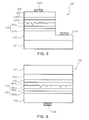
- FIG. 5 is a cross-sectional view of a nitride semiconductor device according to another exemplary embodiment of the present invention.
- FIG. 6 is a cross-sectional view of a nitride semiconductor device according to another exemplary embodiment of the present invention.
- FIGS. 7 and 8 are graphs depicting the quantity of light and the characteristic of reverse bias of a vertical nitride semiconductor device of FIG. 6 respectively, in comparison with the related art.
- FIG. 1 is a cross-sectional view of a nitride semiconductor device according to an exemplary embodiment of the present invention.
- FIG. 2 illustrates the conduction band energy levels of layers illustrated in FIG. 1 , including a thermal stress control layer and a lattice stress control layer.
- a nitride semiconductor device 100 includes a substrate 101 , an n-type nitride semiconductor layer 102 , a thermal stress control layer 103 , a lattice stress control layer 104 , an active layer 105 , and a p-type nitride semiconductor layer 106 .
- An n-type electrode 107 a may be disposed on the exposed surface of the n-type nitride semiconductor layer 102
- a p-type electrode 107 b may be disposed on the top surface of the p-type nitride semiconductor layer 106
- an ohmic contact layer (not shown), formed of a transparent electrode material, may be disposed between the p-type nitride semiconductor layer 106 and the p-type electrode 107 b .
- a horizontal nitride semiconductor device structure is illustrated in which the n-type and p-type electrodes 107 a and 107 b are disposed in the same direction.
- the present invention is not limited thereto, and may be used for a vertical nitride semiconductor device as will be described later. In the vertical nitride semiconductor device, a sapphire substrate may be removed.
- the substrate 101 is provided as a substrate for growing a single nitride crystal, and a sapphire substrate may be used in general.
- the sapphire substrate is a crystal body having Hexa-Rhombo (Hexa-Rhombo R3c) symmetry.
- the sapphire substrate has a lattice constant of 13.001 ⁇ in c-axis orientation, and a lattice constant of 4.765 ⁇ in a-axis orientation, and has a C-plane (0001), an A-plane (1120) and an R-plane (1102).
- a substrate may be formed of Si, SiC, GaN, ZnO, MgAl 2 O 4 , MgO, LiAlO 2 or LiGaO 2 according to shape.
- a buffer layer for example, an un-doped GaN layer may be grown to improve the quality of the nitride-based semiconductor single crystal grown on the substrate 101 .
- the n-type and p-type nitride semiconductor layers 102 and 106 may be formed of n-doped and p-doped semiconductor materials represented by Al x In y Ga (1-x-y) N where 0 ⁇ x ⁇ 1, 0 ⁇ y ⁇ 1, and 0 ⁇ x+y ⁇ 1.
- Representative examples of the semiconductor material include GaN, AlGaN and InGaN.
- the n-type impurities may utilize Si, Ge, Se and Te, and the p-type impurities may utilize Mg, Zn and Be.
- the n-type and p-type nitride semiconductor layers 102 and 106 may be grown by use of a known process such as metal-organic chemical vapor deposition (MOCVD) or hydride vapor phase epitaxy (HVPE).
- MOCVD metal-organic chemical vapor deposition
- HVPE hydride vapor phase epitaxy
- the active layer 105 is disposed between the n-type and p-type nitride semiconductor layers 102 and 106 and emits light with a predetermined energy by electron-hole recombination.
- the active layer 105 may have a multiple quantum well (MQW) structure in which quantum well layers and quantum barrier layers are alternately laminated.
- MQW multiple quantum well
- a structure of InGaN/GaN may be used in general.
- the thermal stress control layer 103 serves to reduce stress caused by variations in the thermal expansion coefficient (CTE) and acting on a nitride semiconductor layer grown on the thermal stress control layer 103 , particularly, on the active layer 105 .
- the thermal stress control layer 103 may be formed of a material having a smaller CTE than the n-type and p-type nitride semiconductor layers 102 and 106 .
- the thermal stress control layer 103 may be formed of a material represented by Al x1 In y1 Ga (1-x1) N where 0 ⁇ x1 ⁇ 1 and 0 ⁇ y1 ⁇ 0.01.
- a nitride semiconductor layer containing Al has a smaller CTE than GaN, thereby reducing the extent to which GaN expands or contracts due to variations in temperature.
- a GaN film, grown on a substrate such as a sapphire substrate is curved concavely due to tensile stress as its thickness increases.
- the GaN film is curved convexly at temperatures lower than the growth temperature of GaN, due to compressive stress.
- the thermal stress control layer 103 formed of a material with a lower CTE than the GaN film is used as in this embodiment, then tensile stress acts on the growing active layer 105 , thereby minimizing influences of the variations in temperature, that is, the curving of the GaN film.
- the thermal stress control layer 103 may have a thickness t 1 of about 100 nm or more.
- a thermal stress control layer may apply compressive stress to an active layer after a substrate serving to grow a nitride single crystal is removed.
- FIG. 3 is a graph depicting variations in wavelength distribution over locations in a wafer according to the embodiment of the present invention and comparative examples of the related art.
- Sample 1 in FIG. 3 represents a general LED structure including none of thermal stress and lattice stress control layers
- sample 2 represents an LED structure employing just a lattice stress control layer
- sample 3 represents an LED structure employing the structure of FIG. 1 , that is, both the thermal stress and lattice stress control layers.
- the composition of the InGaN film varies according to the temperature of a growth plane.
- the extent to which the active layer 105 is curved may be estimated based on differences in an emission wavelength at each spot. It can be seen from FIG. 3 that the LED structure employing the thermal stress control layer as in this embodiment ensures uniform light emission over the entire emission plane since the curving of a nitride film is minimized.
- the thermal stress control layer 103 may serve to alleviate the thermal stress applied to the active layer 105 .
- the thermal stress control layer 103 disposed under the active layer 105 may cause stress due to a difference in the lattice constant therebetween.
- this embodiment employs the lattice stress control layer 104 between the thermal stress control layer 103 and the active layer 105 .
- the lattice stress control layer 104 serves to reduce a difference in the lattice constant between the thermal stress control layer 103 and the active layer 105 .
- the lattice stress control layer 104 may be formed of a material having a band gap energy which is less than that of the thermal stress control layer 103 and greater than that of the quantum well layers of the active layer 105 .
- the lattice stress control layer 104 may be formed of Alx 3 In y3 Ga (1-x3-y3) N where 0 ⁇ x3 ⁇ 1 and 0 ⁇ y3 ⁇ 1 and have a smaller In content than that in the quantum well layer of the active layer 105 . This allows a smaller difference in the lattice constant with the active layer 105 than that between the active layer 105 and the thermal stress control layer 103 .
- the lattice stress control layer 104 may include a first layer 104 a and a second layer 104 b .
- the first layer 104 a may be formed of Al x3 In y3 Ga (1-x3-y3) N where 0 ⁇ x3 ⁇ 1 and 0 ⁇ y3 ⁇ 1 and have a thickness t 2 of about 20 nm in order to alleviate lattice stress.
- the crystalline properties of the first layer 104 a may be undermined in a portion around a threading dislocation. Accordingly, as shown in FIG. 1 , pits are formed in the top surface of the first layer 104 a by removing a portion where crystalline defects, such as threading dislocations, occur. The pits may be formed by etching the top surface of the first layer 104 . In this case, defective portions may be removed first to form pits.
- the etching process may be performed successively with the process of growing a nitride semiconductor in an in-situ process.
- a reaction chamber may be situated in an atmosphere of a gas such as H 2 , N 2 or NH 3 or a combination thereof.
- This in-situ process may favorably affect process efficiency since a growing epi-structure does not need to be moved to the outside of the reaction chamber.
- the second layer 104 b is disposed on the first layer 104 a , filling the pits. To this end, the second layer 104 b has a different composition from the first layer 104 a , and has high crystalline properties.
- the second layer 104 b may be formed of Al x4 In y4 Ga (1-x4-y4) N where 0 ⁇ x4 ⁇ 1 and 0 ⁇ y4 ⁇ y3.
- the use of the second layer 104 b having superior crystalline properties on the defect-removed portion may suppress current leakage, thereby enhancing light emission efficiency.
- FIG. 4 illustrates the intensity of photoluminescence (PL) depending on whether or not a lattice stress control layer is used.
- Sample 3 of FIG. 4 is identical to sample 3 of FIG. 3 , and sample 4 represents a structure including just the thermal stress control layer without the lattice stress control layer. It can be seen from FIG. 4 that the use of both the thermal stress control layer and the lattice stress control layer enhances light emission efficiency.
- FIG. 5 is a cross-sectional view of nitride semiconductor device according to another exemplary embodiment of the present invention.
- a nitride semiconductor device 200 includes a substrate 201 , an n-type nitride semiconductor layer 202 , a thermal stress control layer 203 , a lattice stress control layer 204 , an active layer 205 , and a p-type nitride semiconductor layer 206 .
- An n-type electrode 107 a and a p-type electrode 107 b are formed on the exposed surface of the n-type nitride semiconductor layer 102 and the top surface of the p-type nitride semiconductor layer 106 , respectively.
- the thermal stress control layer 203 includes two layers. That is, as shown in FIG. 5 , the thermal stress control layer 203 includes a third layer 203 a and a fourth layer 203 b .
- the third layer 203 a may be formed of Al x1 In y1 Ga (1-x1) N where 0 ⁇ x1 ⁇ 1 and 0 ⁇ y1 ⁇ 0.01.
- the fourth layer 203 b may be formed of a different material from the third layer 203 a , for example, Al x2 Ga (1-x2) N where 0 ⁇ x2 ⁇ 1.
- the fourth layer 203 b may be disposed between the third layer 203 a serving to alleviate thermal stress and the lattice stress control layer 204 , so that it can alleviate any stress generated between the two layers.
- the active layer 205 has a structure that emits light in a green wavelength range
- a big difference in stress occurs between the lattice stress control layer 204 and the thermal stress control layer, that is, the third layer 203 a , without the fourth layer 203 b . This may degrade the crystalline quality of the lattice stress control layer 204 .
- a semiconductor light emitting device 300 has a vertical electrode structure in which electrodes of opposite polarities are oppositely disposed.
- the semiconductor light emitting device 300 includes an n-type nitride semiconductor layer 302 , a thermal stress control layer 303 , a lattice stress control layer 304 , an active layer 305 , a p-type nitride semiconductor layer 306 , and a conductive substrate 307 .
- the lattice stress control layer 304 includes first and second layers 304 a and 304 b
- the thermal stress control layer 303 includes third and fourth layers 303 a and 303 b .
- a substrate for the growth of a semiconductor single crystal is removed by a laser lift-off process or the like, and an n-type electrode 308 is dispose on the exposed surface of the n-type semiconductor layer 302 after the removal process.
- Like terms may be understood as being designated for like elements throughout embodiments. Thus, a description will be made only about the conductive substrate 307 .
- the conductive substrate 307 serves as both a p-type electrode and a support, which supports a light emission structure, that is, the n-type nitride semiconductor layer 302 , the thermal stress control layer 303 , the lattice stress control layer 304 , the active layer 305 and the p-type nitride semiconductor layer 306 in the laser lift-off process or the like.
- the conductive substrate 307 may be formed of a material such as Si, Cu, Ni, Au, W or Ti.
- the conductive substrate 307 may be formed by plating, bonding or the like according to a selected material.
- a reflective metal layer (not shown) for an ohmic contact and light reflection may be interposed between the p-type nitride semiconductor layer 306 and the conductive layer 307 .
- FIGS. 7 and 8 are graphs depicting the emission quantity and reverse-bias characteristics of the vertical nitride semiconductor device of FIG. 6 respectively, in comparison with the related art.
- the structure according to the present invention is a vertical nitride semiconductor device having 1 mm ⁇ 1 mm chip size, and the structure of the related art corresponds to the structure of FIG. 6 , excluding the thermal stress control layer and the lattice stress control layer.
- the structure of the present invention has emission characteristics improved by about 12% as compared to the related art structure.
- the structure of the present invention realizes the superior characteristics of reverse bias to the related art structure.
- a nitride semiconductor device realizes enhanced emission efficiency by alleviating thermal stress and lattice stress acting on the active layer.
Abstract
Description
Claims (11)
Applications Claiming Priority (2)
| Application Number | Priority Date | Filing Date | Title |
|---|---|---|---|
| KR10-2008-0130075 | 2008-12-19 | ||
| KR1020080130075A KR100990646B1 (en) | 2008-12-19 | 2008-12-19 | Nitride Semiconductor Device |
Publications (2)
| Publication Number | Publication Date |
|---|---|
| US20100155699A1 US20100155699A1 (en) | 2010-06-24 |
| US7973303B2 true US7973303B2 (en) | 2011-07-05 |
Family
ID=42264687
Family Applications (1)
| Application Number | Title | Priority Date | Filing Date |
|---|---|---|---|
| US12/580,152 Active 2030-01-26 US7973303B2 (en) | 2008-12-19 | 2009-10-15 | Nitride semiconductor device |
Country Status (3)
| Country | Link |
|---|---|
| US (1) | US7973303B2 (en) |
| JP (1) | JP5246714B2 (en) |
| KR (1) | KR100990646B1 (en) |
Cited By (2)
| Publication number | Priority date | Publication date | Assignee | Title |
|---|---|---|---|---|
| US9070835B2 (en) | 2013-04-19 | 2015-06-30 | Samsung Electronics Co., Ltd. | Semiconductor light emitting device |
| US9112105B1 (en) | 2014-02-04 | 2015-08-18 | Samsung Electronics Co., Ltd. | Nitride semiconductor light emitting device |
Families Citing this family (7)
| Publication number | Priority date | Publication date | Assignee | Title |
|---|---|---|---|---|
| JP2010225765A (en) * | 2009-03-23 | 2010-10-07 | Panasonic Corp | Semiconductor device and method of manufacturing the same |
| KR101778161B1 (en) * | 2011-01-26 | 2017-09-13 | 엘지이노텍 주식회사 | Light emitting device |
| US20130099357A1 (en) * | 2011-10-21 | 2013-04-25 | Rytis Dargis | Strain compensated reo buffer for iii-n on silicon |
| US10256368B2 (en) * | 2012-12-18 | 2019-04-09 | Sk Siltron Co., Ltd. | Semiconductor substrate for controlling a strain |
| JP6302485B2 (en) * | 2012-12-18 | 2018-03-28 | エスケー シルトロン カンパニー リミテッド | Semiconductor substrate |
| KR20140100115A (en) * | 2013-02-05 | 2014-08-14 | 삼성전자주식회사 | Semiconductor light emitting device |
| KR102506441B1 (en) * | 2017-12-04 | 2023-03-06 | 삼성전자주식회사 | Fabrication method of semiconductor light emitting array and semiconductor light emitting array |
Citations (2)
| Publication number | Priority date | Publication date | Assignee | Title |
|---|---|---|---|---|
| KR20010034578A (en) | 1998-03-12 | 2001-04-25 | 오가와 에지 | Nitride semiconductor device |
| US6635904B2 (en) | 2001-03-29 | 2003-10-21 | Lumileds Lighting U.S., Llc | Indium gallium nitride smoothing structures for III-nitride devices |
Family Cites Families (6)
| Publication number | Priority date | Publication date | Assignee | Title |
|---|---|---|---|---|
| JPS617674A (en) | 1984-06-22 | 1986-01-14 | Nec Corp | Group iii-v compound semiconductor light-emitting element |
| JP3924973B2 (en) * | 1994-12-02 | 2007-06-06 | 日亜化学工業株式会社 | Nitride semiconductor light emitting device manufacturing method and nitride semiconductor light emitting device |
| JP3890930B2 (en) * | 1995-03-29 | 2007-03-07 | 日亜化学工業株式会社 | Nitride semiconductor light emitting device |
| JPH10303510A (en) | 1997-04-23 | 1998-11-13 | Fuji Electric Co Ltd | Iii-group nitride semiconductor device and its manufacture |
| US6423984B1 (en) | 1998-09-10 | 2002-07-23 | Toyoda Gosei Co., Ltd. | Light-emitting semiconductor device using gallium nitride compound semiconductor |
| JP4899632B2 (en) | 2006-05-19 | 2012-03-21 | 日立電線株式会社 | Nitride semiconductor light emitting diode |
-
2008
- 2008-12-19 KR KR1020080130075A patent/KR100990646B1/en active IP Right Grant
-
2009
- 2009-10-15 US US12/580,152 patent/US7973303B2/en active Active
- 2009-10-15 JP JP2009238773A patent/JP5246714B2/en active Active
Patent Citations (2)
| Publication number | Priority date | Publication date | Assignee | Title |
|---|---|---|---|---|
| KR20010034578A (en) | 1998-03-12 | 2001-04-25 | 오가와 에지 | Nitride semiconductor device |
| US6635904B2 (en) | 2001-03-29 | 2003-10-21 | Lumileds Lighting U.S., Llc | Indium gallium nitride smoothing structures for III-nitride devices |
Cited By (2)
| Publication number | Priority date | Publication date | Assignee | Title |
|---|---|---|---|---|
| US9070835B2 (en) | 2013-04-19 | 2015-06-30 | Samsung Electronics Co., Ltd. | Semiconductor light emitting device |
| US9112105B1 (en) | 2014-02-04 | 2015-08-18 | Samsung Electronics Co., Ltd. | Nitride semiconductor light emitting device |
Also Published As
| Publication number | Publication date |
|---|---|
| KR100990646B1 (en) | 2010-10-29 |
| JP5246714B2 (en) | 2013-07-24 |
| US20100155699A1 (en) | 2010-06-24 |
| JP2010147459A (en) | 2010-07-01 |
| KR20100071380A (en) | 2010-06-29 |
Similar Documents
| Publication | Publication Date | Title |
|---|---|---|
| US7973303B2 (en) | Nitride semiconductor device | |
| US8664693B2 (en) | Light emitting diode having algan buffer layer and method of fabricating the same | |
| US8030640B2 (en) | Nitride semiconductor light emitting device and method of manufacturing the same | |
| US8946772B2 (en) | Substrate for epitaxial growth, process for manufacturing GaN-based semiconductor film, GaN-based semiconductor film, process for manufacturing GaN-based semiconductor light emitting element and GaN-based semiconductor light emitting element | |
| US8728841B2 (en) | Method of manufacturing ESD resistant nitride semiconductor light emitting device with enhanced light extraction efficiency | |
| KR100978330B1 (en) | Semiconductor light emitting device and illuminating device using it | |
| US20140191192A1 (en) | Semiconductor light-emitting device | |
| JP2005311374A (en) | Strain-controlled iii-nitride light-emitting device | |
| JP6062966B2 (en) | Gallium nitride light emitting diode | |
| US8269242B2 (en) | Semiconductor light emitting device having surface plasmon layer | |
| US20080042161A1 (en) | Nitride semiconductor light emitting diode | |
| US20160372631A1 (en) | Light emitting diode | |
| US20140103359A1 (en) | Semiconductor light-emitting device and method for manufacturing same | |
| JP2008118049A (en) | GaN-BASED SEMICONDUCTOR LIGHT EMITTING DEVICE | |
| KR101747349B1 (en) | Semiconductor light emitting device | |
| JP4079926B2 (en) | Method of manufacturing ternary nitride buffer layer of nitride light emitting device and method of manufacturing nitride light emitting device | |
| EP2290708B1 (en) | Light-emitting element and a production method therefor | |
| JP2007214378A (en) | Nitride-based semiconductor element | |
| JP2008160025A (en) | Nitride semiconductor light-emitting device | |
| JP2008227103A (en) | GaN-BASED SEMICONDUCTOR LIGHT EMITTING ELEMENT | |
| KR101919109B1 (en) | Uv light emitting deviceand uv light emitting device package | |
| KR20120095652A (en) | Semiconductor light emitting device | |
| KR101417051B1 (en) | A light emitting diode and a method of fabricating the same | |
| KR100730752B1 (en) | Compound semiconductor having supper lattice layer and light emitting diode using the same and method for fabricating the ligth emitting diode | |
| KR20100133157A (en) | Semiconductor light emitting device and manufacturing method of the same |
Legal Events
| Date | Code | Title | Description |
|---|---|---|---|
| AS | Assignment |
Owner name: SAMSUNG LED CO., LTD.,KOREA, REPUBLIC OF Free format text: ASSIGNMENT OF ASSIGNORS INTEREST;ASSIGNORS:SAKONG, TAN;SUNG, YOUN JOON;LEE, JEONG WOOK;REEL/FRAME:023381/0007 Effective date: 20090921 Owner name: SAMSUNG LED CO., LTD., KOREA, REPUBLIC OF Free format text: ASSIGNMENT OF ASSIGNORS INTEREST;ASSIGNORS:SAKONG, TAN;SUNG, YOUN JOON;LEE, JEONG WOOK;REEL/FRAME:023381/0007 Effective date: 20090921 |
|
| FEPP | Fee payment procedure |
Free format text: PAYOR NUMBER ASSIGNED (ORIGINAL EVENT CODE: ASPN); ENTITY STATUS OF PATENT OWNER: LARGE ENTITY |
|
| STCF | Information on status: patent grant |
Free format text: PATENTED CASE |
|
| AS | Assignment |
Owner name: SAMSUNG ELECTRONICS CO., LTD., KOREA, REPUBLIC OF Free format text: MERGER;ASSIGNOR:SAMSUNG LED CO., LTD.;REEL/FRAME:028744/0272 Effective date: 20120403 |
|
| FPAY | Fee payment |
Year of fee payment: 4 |
|
| MAFP | Maintenance fee payment |
Free format text: PAYMENT OF MAINTENANCE FEE, 8TH YEAR, LARGE ENTITY (ORIGINAL EVENT CODE: M1552); ENTITY STATUS OF PATENT OWNER: LARGE ENTITY Year of fee payment: 8 |
|
| MAFP | Maintenance fee payment |
Free format text: PAYMENT OF MAINTENANCE FEE, 12TH YEAR, LARGE ENTITY (ORIGINAL EVENT CODE: M1553); ENTITY STATUS OF PATENT OWNER: LARGE ENTITY Year of fee payment: 12 |