US7948405B2 - Sample rate converter - Google Patents
Sample rate converter Download PDFInfo
- Publication number
- US7948405B2 US7948405B2 US12/578,366 US57836609A US7948405B2 US 7948405 B2 US7948405 B2 US 7948405B2 US 57836609 A US57836609 A US 57836609A US 7948405 B2 US7948405 B2 US 7948405B2
- Authority
- US
- United States
- Prior art keywords
- sampling frequency
- signal
- output
- sample rate
- integrator
- Prior art date
- Legal status (The legal status is an assumption and is not a legal conclusion. Google has not performed a legal analysis and makes no representation as to the accuracy of the status listed.)
- Active
Links
Images


Classifications
-
- H—ELECTRICITY
- H03—ELECTRONIC CIRCUITRY
- H03H—IMPEDANCE NETWORKS, e.g. RESONANT CIRCUITS; RESONATORS
- H03H17/00—Networks using digital techniques
- H03H17/02—Frequency selective networks
- H03H17/06—Non-recursive filters
- H03H17/0621—Non-recursive filters with input-sampling frequency and output-delivery frequency which differ, e.g. extrapolation; Anti-aliasing
- H03H17/0628—Non-recursive filters with input-sampling frequency and output-delivery frequency which differ, e.g. extrapolation; Anti-aliasing the input and output signals being derived from two separate clocks, i.e. asynchronous sample rate conversion
-
- H—ELECTRICITY
- H03—ELECTRONIC CIRCUITRY
- H03H—IMPEDANCE NETWORKS, e.g. RESONANT CIRCUITS; RESONATORS
- H03H17/00—Networks using digital techniques
- H03H17/02—Frequency selective networks
- H03H17/06—Non-recursive filters
- H03H17/0621—Non-recursive filters with input-sampling frequency and output-delivery frequency which differ, e.g. extrapolation; Anti-aliasing
-
- H—ELECTRICITY
- H03—ELECTRONIC CIRCUITRY
- H03H—IMPEDANCE NETWORKS, e.g. RESONANT CIRCUITS; RESONATORS
- H03H17/00—Networks using digital techniques
- H03H17/02—Frequency selective networks
- H03H17/0248—Filters characterised by a particular frequency response or filtering method
- H03H17/028—Polynomial filters
Definitions
- the present invention relates to sample rate converters, and particularly to a sample rate estimator for use in sample rate converters.
- Sample rate converters are devices that are used to convert an input digital signal having a first, input, sample rate to an output digital signal having a different second, output, sample rate. They are common to many different fields of signal processing, including, but not limited to, communications and audio systems. For example, in audio systems and applications, the sample rate of a CD is 44.1 kHz; the sample rate of a digital audio tape (DAT) is typically 48 kHz. Clearly, if data is required to be transferred from CD to DAT, the sample rate must be converted such that the audio can be output at the correct frequency from the DAT, i.e. such that it does not sound “speeded up”.
- ASRC asynchronous sample rate converter
- the ASRC 10 has a rate estimator 12 , which receives a clock signal from the first, input, sample-rate domain, and a clock signal from the second, output, sample-rate domain, and calculates a delay variable a on the basis of the two clock signals.
- a polynomial interpolator 14 receives the delay variable ⁇ and calculates the output signal data samples (i.e. the data having a different sample rate) by interpolating between the input signal data samples using ⁇ . This aspect will be described in greater detail with respect to FIG. 3 .
- an upsampling filter 16 is used to upsample the input data such that the polynomial interpolator 14 is less complex. That is, by increasing the number of data points in the input data, the required accuracy of the interpolation is less, and a lower-order interpolator can be used.
- a downsampling filter 18 is then used to downsample the data output from the interpolator 14 .
- the rate estimator 12 may also calculate a ratio of the input sample rate to the output sample rate. Such a ratio may be useful for other parts of the system in which the sample rate converter 10 is incorporated.
- the rate estimator 12 should converge as quickly as possible to the correct values of the frequency ratio and the delay variable ⁇ , such that the sample rate converter 10 can begin to output data as soon as possible after start up.
- FIG. 2 is a graph illustrating the delay variable a used to calculate the output data.
- an analogue input signal 30 has a smoothly varying amplitude over time.
- An input digital signal is generated by periodically sampling the analogue signal 30 at an input sample rate to obtain input samples (illustrated as solid lines in FIG. 2 ).
- the desired output samples (illustrated by dashed lines in FIG. 2 ) are synchronized with an output clock signal which has a higher frequency than the input clock signal.
- the delay variable a corresponds to the time difference between corresponding samples in the input data and the output data. More specifically, the delay variable a associated with each sample in the output data is the time difference between that sample and the previous sample in the input data.
- ⁇ starts at one and is then ramped down with each sample by an amount that is proportional to the difference between the input and output sample rates.
- ⁇ becomes less than zero, the value of ⁇ wraps with modulo 1, and starts decreasing again from a value just less than one. At the point of wrapping, an additional output sample is generated.
- ⁇ could be defined as being equal to zero initially before being increased to one (the normalized period of the input clock signal), and then wrapping back to zero.
- the polynomial interpolator 14 comprises a buffer that is used to store the input data having an input sample rate FS I .
- FIG. 3 is an illustration of this buffer 20 , which is depicted as a circle in the present case.
- the buffer 20 comprises a number of memory locations, or slots, 22 , in which data samples are stored.
- a read pointer 24 points to a slot which contains data that is to be read out to the polynomial interpolator, and used to calculate a new data sample for the output data having an output sample rate FS O .
- Data is read out of the buffer 20 at the output sample rate FS O .
- a write pointer 26 points to a slot in which input data having the input sample rate FS I is to be written. Data is written to the buffer 20 at the input sample rate FS I .
- the buffer 20 is depicted as a circle, it will be apparent to those skilled in the art that the buffer 20 may take a linear form, with the pointers 24 , 26 cycling back to the first address of the buffer upon reaching the end address of the buffer.
- FS I and FS O are generally different, and thus there necessarily exist mechanisms for preventing the read pointer 24 from catching up with the write pointer 26 or vice versa.
- the output sample rate is higher than the input sample rate.
- the read pointer 24 reads a data sample from the same slot 22 twice. This compensates for the inherent frequency difference between the input sample rate FS I and the output sample rate FS O .
- clock “jitter” short-term variation in the clock frequencies—may cause the write pointer 26 to catch up with the read pointer 24 , or the read pointer 24 to catch up with the write pointer 26 .
- data would be overwritten that has not yet been read.
- an entire buffer's worth of data samples would not be read. Either of these events would cause the sample rate converter 10 to malfunction.
- the rate estimator 12 is to be used to generate read and write pointers for the buffer, it is desirable that these never be equal to one another. That is, the read and write pointers should not point to the same data element in the buffer, causing the sample rate converter 10 to malfunction.
- the sample rate converter 10 should be resistant to such jitter, and continue to output stable values of ⁇ and the frequency ratio, and different values of the read and write pointers, regardless of the jitter in the input clock frequency.
- a sample rate converter circuit for receiving a first signal at a first sampling frequency and for outputting a second signal, representative of said first signal, having a second sampling frequency, said sample rate converter comprising:
- a method of converting a signal sample rate from a first sampling frequency to a second sampling frequency comprising:
- a sample rate converter circuit for receiving a first signal having a first sampling frequency and for outputting a second signal, representative of said first signal, having a second sampling frequency, said sample rate converter comprising:
- a sample rate converter circuit adapted to receive a first signal having a first sampling frequency and to output a second signal, representative of said first signal, having a second sampling frequency, said sample rate converter comprising:
- a signal processing circuit comprising an input for receiving a first signal at a first sampling frequency and an output for outputting a second signal, representative of said first signal, at a second sampling frequency, said signal processing circuit comprising a sample rate converter circuit in accordance with the first or third aspect of the invention.
- FIG. 1 is a block schematic diagram of an asynchronous sample rate converter
- FIG. 2 illustrates sample positions of the input and output samples
- FIG. 3 illustrates a buffer in the polynomial interpolator of FIG. 1 ;
- FIG. 4 shows a first rate estimator for use in the sample rate converter of FIG. 1 ;
- FIG. 5 shows a second rate estimator for use in the sample rate converter of FIG. 1 .
- FIG. 6 shows a third rate estimator for use in the sample rate converter of FIG. 1 ;
- FIG. 7 shows a signal processing device in accordance with a further aspect of the invention.
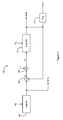
- FIG. 4 illustrates an example of a rate estimator 100 for use as the rate estimator 12 in the sample rate converter 10 of FIG. 1 .
- the rate estimator 100 comprises an input integrator 102 that receives a clock signal having a frequency FS I corresponding to the sample rate of the input signal.
- the input integrator 102 essentially acts as a counter, therefore, clocked at the frequency FS I .
- the output “Write” of the input integrator 102 is used to generate a write pointer for writing data to a buffer, for example as illustrated in FIG. 3 .
- a certain number of least-significant bits (LSBs) of the output of the input integrator 102 may be used for this purpose.
- LSBs least-significant bits
- three LSBs may be used to define the write pointer.
- the output of the input integrator 102 is also fed to a control loop.
- a feedback signal is subtracted from the output of the input integrator 102 in an adding element 104 , generating an error signal e.
- the error signal e is multiplied by a gain coefficient K in a multiplying element 106 to generate a signal R which, as will be shown in more detail later, is an estimate of the ratio of the input sample rate and the output sample rate.
- the output R of the multiplying element 106 is input to an output integrator 110 , which receives a clock signal having a frequency corresponding to the output sample rate FS O .
- the output integrator 110 is therefore clocked at FS O .
- the output of the output integrator 110 may be used to generate a read pointer “Read” similar to the generation of the write pointer described above. That is, a certain number of LSBs may be used to define the read pointer. In fact, since the output integrator is able to generate a fractional output, the desired number of integer bits is used to define the read pointer.
- the output of the output integrator 110 is passed back to the adding element 104 for use as the feedback signal mentioned above.
- the output of the output integrator 110 is also applied to a filter 112 , which is used to separate off the fractional part of the signal, which is then used as the value of the delay variable ⁇ .
- the output of the input integrator 102 increments by 1.
- the output of the output integrator 110 increments by R.
- the rate of change of the output of the input integrator 102 is equal to L ⁇ FS I , where L is the upsampling factor of the upsampling filter 16 in FIG. 1 .
- the rate of change of the output of the output integrator 110 is equal to R ⁇ M ⁇ FS O , where M is equal to the downsampling factor of the downsampling filter 18 in FIG. 1 .
- the value of R stabilises by negative feedback. If the value of R is too low, the rate of change of the output integrator 110 reduces, and therefore the output of the error adding element 104 increases, causing R to increase again.
- R L . FS l M . FS O
- R is an estimate of the ratio of the input sample rate and the output sample rate (modified by the upsampling L and downsampling M).
- the fractional part of R is also equal to step size of the ⁇ -value needed by the polynomial interpolator 14 . Therefore the value of ⁇ can easily be obtained by first integrating R(n) then obtaining the fractional part.
- the read pointer for the buffers must change at the same time that the ⁇ -value wraps. This property is observed in the integer part of the output of the output integrator 110 .
- the integer part of the output of the output integrator 110 can be used to generate the read pointer.
- rate estimator 100 described with respect to FIG. 4 suffers from a number of problems.
- the write and read pointers are derived from the respective outputs of the integrators 102 , 110 , and it can be shown that the difference between the write and read pointers (the pointer offset, P O ) is equal to
- the loop attenuates jitter on the input FS I clock for FS I frequencies above a cutoff frequency that is defined by the value of K. That is, it ensures that variations in the clock timing compared to ideal regular clock instants do not affect the accuracy of the ⁇ value.
- the read pointer is also derived from the control loop, the read pointer is stable too and not affected by jitter on the input clock.
- the write pointer may move backwards and forwards relative to an “ideal” value.
- the read pointer is relatively stable, this means that the write pointer may catch up with the read pointer, causing the sample rate converter to malfunction as described above. Since the pointer offset is dependent on sample-rate ratio, it is not possible to guarantee how much jitter can be tolerated before the pointers catch up and the converter malfunctions.
- K i.e. R needs to be within N.K of its final value to guarantee that no glitches occur. Since K has a very low value it takes several hundred milliseconds before the loop has settled adequately to guarantee that pointer collisions cannot occur. This is an unacceptably long time in many applications.
- the convergence time is inversely proportional to the value of K.
- K results in a relatively short convergence time.
- a high value of K also causes considerable “ripple” in the output of the control loop. That is, a high value of K will cause the output to reach the correct output value quickly, but overshoot and oscillate about the converged output value.
- the ripple will cause a high level of distortion in the sample-rate converter since the value of a will fluctuate from sample-to-sample.
- a high value of K also has the disadvantage that the loop cutoff frequency is higher and the jitter attenuation is poor.
- FIG. 5 illustrates a rate estimator 200 according to the present invention.
- the rate estimator 200 is similar to the rate estimator 100 described with respect to FIG. 4 .
- Components having similar reference numerals are similar to their counterparts in FIG. 4 , and so will not be further described herein.
- the gain value K applied in the multiplying element 106 is adapted to improve the convergence time of the loop, without producing substantial oscillation in the output of the control loop. This is achieved by starting with a relatively high value of K, and then reducing that value as the output value approaches the correct value.
- K may take an initial value (e.g. 0.5), and then its value halves for every doubling of sampling time.
- initial value e.g. 0.5
- K may take an initial value (e.g. 0.5), and then its value halves for every doubling of sampling time.
- a person skilled in the art will be able to think of many schemes whereby the value of K is reduced over time.
- the value of K is repeatedly halved, under the control of a control block 208 .
- the value of K may be halved whenever the elapsed sampling time doubles.
- the rate estimator 200 doubles the value of e, the signal output from the adding element 104 , for the sample immediately after the K value is changed. This is achieved by means of an adding element 202 , which subtracts the output of the input integrator 102 from the output of the output integrator 110 , which must be a delaying integrator.
- the output of the adding element 202 is selectively added to the output of the output integrator 110 in another adding element 204 . This has the effect of doubling the value of the signal e when the output of the adder 204 is subtracted from the output of the input integrator 102 in the adder 104 .
- a switch 206 also operating under the control of the control block 208 , is employed so that the output of the adding element 202 is added to the output of the output integrator 110 (and hence the signal e is doubled) only when the K value is changed.
- the control block 208 ensures that the switch 206 is closed when the K value is changed, and kept open otherwise.
- the rate estimator 200 therefore overcomes the problem of slow convergence to the correct output value.
- the convergence of the control loop is initially quick, but then slowed to prevent ripple in the output value. No jumps are experienced in the output signal when the value of K changes, by appropriate compensation of the error signal on the samples immediately after the K value is changed.
- the adaption of K takes place upon start-up of the sample rate converter.
- the adaption of K may also take place if it is detected that the output value has drifted significantly from an ideal value, for example.
- FIG. 6 shows a further rate estimator 300 according to the present invention.
- the rate estimator 300 uses an architecture with two blocks 302 , 304 containing respective control loops to overcome the problem of the read and write pointers overtaking one another and prevent the offset being dependent on the sample-rate ratio.
- the loop in one of the blocks 302 uses an adaptive value of K as described above, so that the circuit quickly converges to the correct output value.
- the rate estimator 300 comprises a first block 302 whose function is to generate an estimate of the frequency ratio between the input and output sample rates for use as an offset in a second block 304 .
- the first block 302 comprises an input integrator 306 that receives a clock signal FS I having a frequency corresponding to the input sample rate.
- the input integrator 306 therefore operates as a counter.
- the output of the input integrator 306 is fed to a control loop.
- a feedback signal is subtracted from the output of the input integrator 306 in an adding element 308 , generating an error signal e.
- the error signal e is multiplied by a gain coefficient K in a multiplying element 310 to generate a signal R′ which, as was shown previously with respect to FIG.
- the signal R′ is input to an output integrator 314 , which is clocked at a frequency corresponding to the output sample rate FS O .
- the output of the output integrator 314 is used as the feedback signal mentioned above with respect to the adding element 308 .
- the value of K is adapted as mentioned previously with respect to FIG. 5 , under the control of a control block 322 .
- adding elements 316 , 318 and a switch 320 are included, corresponding to adding elements 202 , 204 and switch 206 in FIG. 5 , with the switch 320 also being controlled by the control block 322 .
- the error signal e is doubled by closing the switch 320 .
- the rate estimator 300 further comprises a second block 304 .
- a further input integrator 340 is provided, also being clocked at the frequency FS I corresponding to the input sample rate.
- the output of the input integrator 340 is used to generate a write pointer “Write” for writing data to a buffer, for example as illustrated in FIG. 3 .
- a certain number of least-significant bits (LSBs) of the output of the input integrator 340 may be used for this purpose. In a relatively simple example where the buffer has eight data slots, three LSBs may be used to define the write pointer.
- the output of the input integrator 340 is also fed to a control loop.
- a feedback signal is subtracted from the output of the input integrator 340 in an adding element 342 , generating an error signal E.
- the error signal E is multiplied by a gain coefficient K′ in a multiplying element 344 , with the value of K′ again being controlled by the control block 322 .
- the value of K′ is typically 1 ⁇ 8 of the value of K used in the first control loop, and thus the value of K′ is varied as the value of K is varied.
- the value of K′ may be kept the same as the value of K used in the first control loop, but the first loop may be run 8 times as fast as the second loop. Other combinations of ratios of the multiplying values and the loop rates are also possible.
- the output of the multiplying element 344 is added in an adding element 346 to the signal R′, output from the multiplying element 310 in the first loop 302 .
- the output of the adding element 346 is input to an output integrator 350 , which is clocked at a frequency corresponding to the output sample rate FS O .
- the output of the output integrator 350 may be used to generate a read pointer.
- an extra offset is required to be added to the output integrator 350 output in an adding element 352 . This aspect will be described in greater detail below.
- the output of the adding element 352 may then be used to generate the read pointer “Read”, similar to the generation of the write pointer described above. That is, a certain number of LSBs from the integer part of the word may be used to define the read pointer.
- the output of the output integrator 350 is further used as the feedback signal mentioned above with respect to the adding element 342 .
- the output of the output integrator 350 is also used to generate the value of the delay variable ⁇ , by taking the fractional part of the signal in a filter 354 .
- one of the actions of the first loop 302 is to generate a signal R′ that is an estimate of the ratio of the input and output sample rates. This is then supplied to the second loop 304 as an offset.
- the first loop 302 also comprises an adaptive value of K, with appropriate compensation to the error signal e, such that the output of the control loop 302 rapidly and smoothly converges to a stable value of R′.
- the adaptive value of K is not necessary for this embodiment to operate correctly.
- the error signal E output from the adding element 342 is driven substantially to zero.
- the read pointer “Read” and the write pointer “Write” are derived from the outputs of the output integrator 350 and the input integrator 340 , respectively. Therefore, if the error signal E is zero, the offset between the read and write pointers is zero, and independent of the sample-rate ratio.
- the read and write pointers are the same, and therefore an offset is added in the adding element 352 , before generating the read pointer “Read”.
- the offset is equal to half the length of the buffer, in order that the pointers should be spaced as far apart as possible.
- the pointers are maximally tolerant to short-term variations, or jitter, in the sample-rate ratio.
- the loop circuits may be adapted such that the time constants of each loop differ from each other. As mentioned above, this may be achieved by running the loops at different frequencies, by utilizing different values of K in each loop, or a combination of these. As an alternative example, the loop in the first block 302 may be run at four times the frequency of the loop in the second block 304 , and the K′ value used in the second block 304 may be half the K value used in the first block 302 .
- the present invention has therefore provided a rate estimator with an adaptive gain coefficient to ensure that a control loop converges as quickly as possible to a stable output value.
- compensation is provided for the sample immediately following adjustment of the K value, so that the output value is smoothly adapted.
- a rate estimator is provided with a dual-loop architecture.
- a first loop of the rate estimator generates a ratio of an input sample rate to an output sample rate and provides that ratio to a second loop as a first offset.
- the second loop generates read and write pointers for access to a buffer containing sample data, where the first offset ensures that a second offset between the read and write pointers is substantially independent of the sample-rate ratio.
- switches described herein can be implemented in a number of different ways (for example, MOS transistor switches or MOS transmission gate switches) depending upon, for example, an integrated circuit's process technology or the input and output voltage requirements.
- the sample rate converters described herein are preferably incorporated in an integrated circuit.
- the integrated circuit may be part of an audio and/or video system, such as an MP3 player, a mobile phone, a camera or a satellite navigation system, and the system can be portable (such as a battery-powered handheld system) or can be mains-powered (such as a hi-fi system or a television receiver) or can be an in-car, in-train, or in-plane entertainment system.
- FIG. 7 shows a signal processing device in the form of an audio codec 400 .
- the audio codec 400 has input/output circuitry 402 for digital data, connected to data path switching circuitry 404 , operating under the control of control circuitry 406 .
- the audio codec 400 also has an input for analogue data connected through an analogue-digital converter (ADC) 408 to the data path switching circuitry 404 , and an output for analogue data connected through a digital-analogue converter (DAC) 410 to the data path switching circuitry 404 .
- a sample rate converter 412 is connected to the data path switching circuitry 404 , to allow digital data at one sample rate to be converted to digital data at a second sample rate.
- the sample rate converter is of the general form shown in FIG. 1 , incorporating a rate estimator which may be as shown in FIG. 4
- processor control code for example on a carrier medium such as a disk, CD- or DVD-ROM, programmed memory such as read only memory (firmware), or on a data carrier such as an optical or electrical signal carrier.
- a carrier medium such as a disk, CD- or DVD-ROM, programmed memory such as read only memory (firmware), or on a data carrier such as an optical or electrical signal carrier.
- embodiments of the invention will be implemented on a DSP (digital signal processor), ASIC (application specific integrated circuit) or FPGA (field programmable gate array).
- the code may comprise conventional program code or microcode or, for example code for setting up or controlling an ASIC or FPGA.
- the code may also comprise code for dynamically configuring re-configurable apparatus such as re-programmable logic gate arrays.
- the code may comprise code for a hardware description language such as VerilogTM or VHDL (very high speed integrated circuit hardware description language).
- VerilogTM very high speed integrated circuit hardware description language
- VHDL very high speed integrated circuit hardware description language
- the code may be distributed between a plurality of coupled components in communication with one another.
- the embodiments may also be implemented using code running on a field-(re-)programmable analogue array or similar device in order to configure analogue/digital hardware.
Landscapes
- Physics & Mathematics (AREA)
- Mathematical Physics (AREA)
- Engineering & Computer Science (AREA)
- Computer Hardware Design (AREA)
- Algebra (AREA)
- General Physics & Mathematics (AREA)
- Pure & Applied Mathematics (AREA)
- Analogue/Digital Conversion (AREA)
Abstract
Description
-
- a buffer, for storing data samples received from said first signal;
- a first loop circuit, for receiving a first clock signal corresponding to said first sampling frequency and a second clock signal corresponding to said second sampling frequency, and for generating an estimate of a ratio of the first sampling frequency to the second sampling frequency; and
- a second loop circuit, for receiving said first clock signal, said second clock signal and said estimate of the ratio of the first sampling frequency to the second sampling frequency, and for outputting a write pointer so that said data samples can be stored in the buffer, and for outputting a read pointer so that said data samples can be read from the buffer,
- with a first offset between said read pointer and said write pointer, such that said first offset is substantially independent of said ratio of the first sampling frequency to the second sampling frequency.
-
- receiving a first signal at the first sampling frequency;
- storing in a buffer data samples received from said first signal;
- receiving a first clock signal corresponding to said first sampling frequency and a second clock signal corresponding to said second sampling frequency in a first loop circuit, and generating an estimate of a ratio of the first sampling frequency to the second sampling frequency; and
- receiving said first clock signal, said second clock signal and said estimate of the ratio of the first sampling frequency to the second sampling frequency in a second loop circuit; and
- outputting a write pointer so that said data samples can be stored in the buffer, and outputting a read pointer so that said data samples can be read from the buffer, with a first offset between said read pointer and said write pointer, such that said first offset is substantially independent of said ratio of the first sampling frequency to the second sampling frequency.
-
- a loop circuit, for receiving a first clock signal corresponding to said first sampling frequency and a second clock signal corresponding to said second sampling frequency, and for generating an estimate of a frequency ratio of the first sampling frequency to the second sampling frequency, wherein the loop circuit comprises:
- a multiplier, for multiplying an error signal of the loop circuit by a gain coefficient, wherein said gain coefficient is dynamically adjusted to change the rate of convergence of the loop circuit to the estimate of the frequency ratio,
- wherein the circuit is adapted to compensate for the adjustment of the gain coefficient by correspondingly adjusting said error signal.
-
- a loop circuit, for receiving a first clock signal corresponding to said first sampling frequency and a second clock signal corresponding to said second sampling frequency, and for generating an estimate of a frequency ratio of the first sampling frequency to the second sampling frequency, wherein the loop circuit comprises:
- a multiplier, for multiplying an error signal of the loop circuit by a gain coefficient,
- wherein the method comprises dynamically adjusting said gain coefficient to change the rate of convergence of the loop circuit to the estimate of the frequency ratio,
- and further comprises compensating for the adjustment of the gain coefficient by correspondingly adjusting said error signal.
and R is an estimate of the ratio of the input sample rate and the output sample rate (modified by the upsampling L and downsampling M). Hence the fractional part of R is also equal to step size of the α-value needed by the
where N is the length of the buffer. The pointer offset is therefore dependent on the sample-rate ratio. Since the sample rate ratio varies according to the application, and may also drift over time, it is not possible to guarantee that pointer collision cannot occur.
i.e. R needs to be within N.K of its final value to guarantee that no glitches occur. Since K has a very low value it takes several hundred milliseconds before the loop has settled adequately to guarantee that pointer collisions cannot occur. This is an unacceptably long time in many applications.
Claims (20)
Applications Claiming Priority (3)
| Application Number | Priority Date | Filing Date | Title |
|---|---|---|---|
| GB0818759.3 | 2008-10-13 | ||
| GB08187593 | 2008-10-13 | ||
| GB0818759A GB2456360B (en) | 2008-10-13 | 2008-10-13 | Sample rate converter |
Publications (2)
| Publication Number | Publication Date |
|---|---|
| US20100091922A1 US20100091922A1 (en) | 2010-04-15 |
| US7948405B2 true US7948405B2 (en) | 2011-05-24 |
Family
ID=40083956
Family Applications (1)
| Application Number | Title | Priority Date | Filing Date |
|---|---|---|---|
| US12/578,366 Active US7948405B2 (en) | 2008-10-13 | 2009-10-13 | Sample rate converter |
Country Status (2)
| Country | Link |
|---|---|
| US (1) | US7948405B2 (en) |
| GB (1) | GB2456360B (en) |
Cited By (2)
| Publication number | Priority date | Publication date | Assignee | Title |
|---|---|---|---|---|
| US20110280354A1 (en) * | 2010-05-13 | 2011-11-17 | Den-Kai Juang | Frame timing controller and frame timing control method for triggering at least receiver in mobile station to start receiving transmitted information of base station by referring to at least frame pointer |
| US20150145585A1 (en) * | 2013-11-26 | 2015-05-28 | Richtek Technology Corporation | Sample Rate Converter and Rate Estimator Thereof and Rate Estimation Method Thereof |
Families Citing this family (7)
| Publication number | Priority date | Publication date | Assignee | Title |
|---|---|---|---|---|
| US8737532B2 (en) * | 2012-05-31 | 2014-05-27 | Silicon Laboratories Inc. | Sample rate estimator for digital radio reception systems |
| CN104682918A (en) * | 2013-11-29 | 2015-06-03 | 立锜科技股份有限公司 | Sampling rate converter and ratio estimator used therein and ratio estimation method thereof |
| DE102015110275B4 (en) | 2015-06-25 | 2025-11-20 | Apple Inc. | Devices and methods for shifting a digital signal by a shift time to provide a shifted signal |
| US9768948B2 (en) * | 2015-09-23 | 2017-09-19 | Ibiquity Digital Corporation | Method and apparatus for time alignment of analog and digital pathways in a digital radio receiver |
| US10805183B2 (en) * | 2016-05-31 | 2020-10-13 | Octo Telematics S.P.A. | Method and apparatus for sampling rate conversion of a stream of samples |
| JP7164810B2 (en) * | 2018-09-06 | 2022-11-02 | 日本電信電話株式会社 | Signal processor and optical receiver |
| TWI718808B (en) * | 2019-12-16 | 2021-02-11 | 瑞昱半導體股份有限公司 | Interference canceller and method for cancelling interference |
Citations (9)
| Publication number | Priority date | Publication date | Assignee | Title |
|---|---|---|---|---|
| EP0323200A2 (en) | 1987-12-29 | 1989-07-05 | Sony Corporation | Circuit and method for sampling frequency conversion |
| US6005901A (en) | 1997-02-27 | 1999-12-21 | Advanced Micro Devices | Arrangement for asynchronous decimation using a frequency ratio estimator and method thereof |
| US6061704A (en) * | 1997-12-23 | 2000-05-09 | Telefonaktiebolaget Lm Ericsson | Method and apparatus for rate conversion |
| US6208671B1 (en) * | 1998-01-20 | 2001-03-27 | Cirrus Logic, Inc. | Asynchronous sample rate converter |
| US20020105448A1 (en) | 2001-02-06 | 2002-08-08 | Markus Freidhof | Device and method for conversion of sampling rate |
| US6518894B2 (en) * | 2001-02-12 | 2003-02-11 | Rohde & Schwarz Gmbh & Co. Kg | Device and method for sampling rate conversion |
| GB2386806A (en) | 2002-03-22 | 2003-09-24 | Motorola Inc | Asynchronous sampling rate conversion |
| US6747858B1 (en) | 2002-12-31 | 2004-06-08 | Texas Instruments Incorporated | Digital sample rate converter architecture |
| US20040120361A1 (en) | 2002-12-20 | 2004-06-24 | Texas Instruments Incorporated | Asynchronous sample rate converter and method |
-
2008
- 2008-10-13 GB GB0818759A patent/GB2456360B/en active Active
-
2009
- 2009-10-13 US US12/578,366 patent/US7948405B2/en active Active
Patent Citations (9)
| Publication number | Priority date | Publication date | Assignee | Title |
|---|---|---|---|---|
| EP0323200A2 (en) | 1987-12-29 | 1989-07-05 | Sony Corporation | Circuit and method for sampling frequency conversion |
| US6005901A (en) | 1997-02-27 | 1999-12-21 | Advanced Micro Devices | Arrangement for asynchronous decimation using a frequency ratio estimator and method thereof |
| US6061704A (en) * | 1997-12-23 | 2000-05-09 | Telefonaktiebolaget Lm Ericsson | Method and apparatus for rate conversion |
| US6208671B1 (en) * | 1998-01-20 | 2001-03-27 | Cirrus Logic, Inc. | Asynchronous sample rate converter |
| US20020105448A1 (en) | 2001-02-06 | 2002-08-08 | Markus Freidhof | Device and method for conversion of sampling rate |
| US6518894B2 (en) * | 2001-02-12 | 2003-02-11 | Rohde & Schwarz Gmbh & Co. Kg | Device and method for sampling rate conversion |
| GB2386806A (en) | 2002-03-22 | 2003-09-24 | Motorola Inc | Asynchronous sampling rate conversion |
| US20040120361A1 (en) | 2002-12-20 | 2004-06-24 | Texas Instruments Incorporated | Asynchronous sample rate converter and method |
| US6747858B1 (en) | 2002-12-31 | 2004-06-08 | Texas Instruments Incorporated | Digital sample rate converter architecture |
Cited By (3)
| Publication number | Priority date | Publication date | Assignee | Title |
|---|---|---|---|---|
| US20110280354A1 (en) * | 2010-05-13 | 2011-11-17 | Den-Kai Juang | Frame timing controller and frame timing control method for triggering at least receiver in mobile station to start receiving transmitted information of base station by referring to at least frame pointer |
| US8879585B2 (en) * | 2010-05-13 | 2014-11-04 | Mediatek Inc. | Frame timing controller and frame timing control method for triggering at least receiver in mobile station to start receiving transmitted information of base station by referring to at least frame pointer |
| US20150145585A1 (en) * | 2013-11-26 | 2015-05-28 | Richtek Technology Corporation | Sample Rate Converter and Rate Estimator Thereof and Rate Estimation Method Thereof |
Also Published As
| Publication number | Publication date |
|---|---|
| GB2456360A (en) | 2009-07-15 |
| GB2456360B (en) | 2009-12-02 |
| US20100091922A1 (en) | 2010-04-15 |
| GB0818759D0 (en) | 2008-11-19 |
Similar Documents
| Publication | Publication Date | Title |
|---|---|---|
| US7948405B2 (en) | Sample rate converter | |
| US10623014B2 (en) | Apparatuses and methods for sample rate conversion | |
| US9225353B2 (en) | Apparatuses and methods for linear to discrete quantization conversion with reduced sampling-variation errors | |
| US9000967B2 (en) | Apparatuses and methods for linear to discrete quantization conversion with reduced sampling variation errors | |
| US10263628B2 (en) | Apparatuses and methods for converting fluctuations in periodicity of an input signal into fluctuations in amplitude of an output signal | |
| US7816963B1 (en) | Phase interpolator with adaptive delay adjustment | |
| US9973172B2 (en) | Digital signal processor | |
| US6005901A (en) | Arrangement for asynchronous decimation using a frequency ratio estimator and method thereof | |
| US8730079B2 (en) | Sampling rate converter data flow control mechanism | |
| US7733151B1 (en) | Operating clock generation system and method for audio applications | |
| CN112564701B (en) | Integrated circuit chip and device including integrated circuit chip | |
| US20080315928A1 (en) | Digital phase locked loop with dithering | |
| US9705515B1 (en) | Digital phase locked loop and method of driving the same | |
| US6324235B1 (en) | Asynchronous sample rate tracker | |
| EP3001567B1 (en) | Phase tracker for a phase locked loop | |
| US7414550B1 (en) | Methods and systems for sample rate conversion and sample clock synchronization | |
| US8217812B2 (en) | Adjustable sampling rate converter | |
| US20120054454A1 (en) | Sampling frequency converter | |
| GB2464169A (en) | Sample rate converter with gain and error adjustment | |
| US9356767B1 (en) | Hybrid analog/digital clock recovery system | |
| US7570727B2 (en) | Data transmission controller and sampling frequency converter | |
| US9209783B2 (en) | Efficient drift avoidance mechanism for synchronous and asynchronous digital sample rate converters | |
| CA3259538C (en) | Method and apparatus for synchronizing frequency in remote terminals | |
| US20250310699A1 (en) | Idle tone mitigation using clock jitter | |
| JP2024151297A (en) | PLL circuit |
Legal Events
| Date | Code | Title | Description |
|---|---|---|---|
| AS | Assignment |
Owner name: WOLFSON MICROELECTRONICS PLC,UNITED KINGDOM Free format text: ASSIGNMENT OF ASSIGNORS INTEREST;ASSIGNOR:MAGRATH, ANTHONY;REEL/FRAME:023365/0774 Effective date: 20091012 Owner name: WOLFSON MICROELECTRONICS PLC, UNITED KINGDOM Free format text: ASSIGNMENT OF ASSIGNORS INTEREST;ASSIGNOR:MAGRATH, ANTHONY;REEL/FRAME:023365/0774 Effective date: 20091012 |
|
| STCF | Information on status: patent grant |
Free format text: PATENTED CASE |
|
| FEPP | Fee payment procedure |
Free format text: PAT HOLDER NO LONGER CLAIMS SMALL ENTITY STATUS, ENTITY STATUS SET TO UNDISCOUNTED (ORIGINAL EVENT CODE: STOL); ENTITY STATUS OF PATENT OWNER: LARGE ENTITY |
|
| FPAY | Fee payment |
Year of fee payment: 4 |
|
| AS | Assignment |
Owner name: CIRRUS LOGIC INTERNATIONAL (UK) LTD., UNITED KINGD Free format text: CHANGE OF NAME;ASSIGNOR:WOLFSON MICROELECTRONICS LTD;REEL/FRAME:035353/0413 Effective date: 20141127 Owner name: WOLFSON MICROELECTRONICS LTD, UNITED KINGDOM Free format text: CHANGE OF NAME;ASSIGNOR:WOLFSON MICROELECTRONICS PLC;REEL/FRAME:035356/0096 Effective date: 20140821 |
|
| AS | Assignment |
Owner name: CIRRUS LOGIC INTERNATIONAL SEMICONDUCTOR LTD., UNI Free format text: ASSIGNMENT OF ASSIGNORS INTEREST;ASSIGNOR:CIRRUS LOGIC INTERNATIONAL (UK) LTD.;REEL/FRAME:035806/0389 Effective date: 20150329 |
|
| AS | Assignment |
Owner name: CIRRUS LOGIC INC., TEXAS Free format text: ASSIGNMENT OF ASSIGNORS INTEREST;ASSIGNOR:CIRRUS LOGIC INTERNATIONAL SEMICONDUCTOR LTD.;REEL/FRAME:035909/0190 Effective date: 20150329 |
|
| MAFP | Maintenance fee payment |
Free format text: PAYMENT OF MAINTENANCE FEE, 8TH YEAR, LARGE ENTITY (ORIGINAL EVENT CODE: M1552); ENTITY STATUS OF PATENT OWNER: LARGE ENTITY Year of fee payment: 8 |
|
| MAFP | Maintenance fee payment |
Free format text: PAYMENT OF MAINTENANCE FEE, 12TH YEAR, LARGE ENTITY (ORIGINAL EVENT CODE: M1553); ENTITY STATUS OF PATENT OWNER: LARGE ENTITY Year of fee payment: 12 |