US7936326B2 - Apparatus and method for LCD panel drive for achieving time-divisional driving and inversion driving - Google Patents
Apparatus and method for LCD panel drive for achieving time-divisional driving and inversion driving Download PDFInfo
- Publication number
- US7936326B2 US7936326B2 US11/142,415 US14241505A US7936326B2 US 7936326 B2 US7936326 B2 US 7936326B2 US 14241505 A US14241505 A US 14241505A US 7936326 B2 US7936326 B2 US 7936326B2
- Authority
- US
- United States
- Prior art keywords
- data
- data lines
- data line
- lines
- pixels
- Prior art date
- Legal status (The legal status is an assumption and is not a legal conclusion. Google has not performed a legal analysis and makes no representation as to the accuracy of the status listed.)
- Active, expires
Links
Images


Classifications
-
- G—PHYSICS
- G09—EDUCATION; CRYPTOGRAPHY; DISPLAY; ADVERTISING; SEALS
- G09G—ARRANGEMENTS OR CIRCUITS FOR CONTROL OF INDICATING DEVICES USING STATIC MEANS TO PRESENT VARIABLE INFORMATION
- G09G3/00—Control arrangements or circuits, of interest only in connection with visual indicators other than cathode-ray tubes
- G09G3/20—Control arrangements or circuits, of interest only in connection with visual indicators other than cathode-ray tubes for presentation of an assembly of a number of characters, e.g. a page, by composing the assembly by combination of individual elements arranged in a matrix no fixed position being assigned to or needed to be assigned to the individual characters or partial characters
- G09G3/34—Control arrangements or circuits, of interest only in connection with visual indicators other than cathode-ray tubes for presentation of an assembly of a number of characters, e.g. a page, by composing the assembly by combination of individual elements arranged in a matrix no fixed position being assigned to or needed to be assigned to the individual characters or partial characters by control of light from an independent source
- G09G3/36—Control arrangements or circuits, of interest only in connection with visual indicators other than cathode-ray tubes for presentation of an assembly of a number of characters, e.g. a page, by composing the assembly by combination of individual elements arranged in a matrix no fixed position being assigned to or needed to be assigned to the individual characters or partial characters by control of light from an independent source using liquid crystals
- G09G3/3611—Control of matrices with row and column drivers
- G09G3/3685—Details of drivers for data electrodes
- G09G3/3688—Details of drivers for data electrodes suitable for active matrices only
-
- G—PHYSICS
- G09—EDUCATION; CRYPTOGRAPHY; DISPLAY; ADVERTISING; SEALS
- G09G—ARRANGEMENTS OR CIRCUITS FOR CONTROL OF INDICATING DEVICES USING STATIC MEANS TO PRESENT VARIABLE INFORMATION
- G09G3/00—Control arrangements or circuits, of interest only in connection with visual indicators other than cathode-ray tubes
- G09G3/20—Control arrangements or circuits, of interest only in connection with visual indicators other than cathode-ray tubes for presentation of an assembly of a number of characters, e.g. a page, by composing the assembly by combination of individual elements arranged in a matrix no fixed position being assigned to or needed to be assigned to the individual characters or partial characters
- G09G3/34—Control arrangements or circuits, of interest only in connection with visual indicators other than cathode-ray tubes for presentation of an assembly of a number of characters, e.g. a page, by composing the assembly by combination of individual elements arranged in a matrix no fixed position being assigned to or needed to be assigned to the individual characters or partial characters by control of light from an independent source
- G09G3/36—Control arrangements or circuits, of interest only in connection with visual indicators other than cathode-ray tubes for presentation of an assembly of a number of characters, e.g. a page, by composing the assembly by combination of individual elements arranged in a matrix no fixed position being assigned to or needed to be assigned to the individual characters or partial characters by control of light from an independent source using liquid crystals
- G09G3/3611—Control of matrices with row and column drivers
- G09G3/3614—Control of polarity reversal in general
-
- G—PHYSICS
- G09—EDUCATION; CRYPTOGRAPHY; DISPLAY; ADVERTISING; SEALS
- G09G—ARRANGEMENTS OR CIRCUITS FOR CONTROL OF INDICATING DEVICES USING STATIC MEANS TO PRESENT VARIABLE INFORMATION
- G09G2310/00—Command of the display device
- G09G2310/02—Addressing, scanning or driving the display screen or processing steps related thereto
- G09G2310/0202—Addressing of scan or signal lines
- G09G2310/0218—Addressing of scan or signal lines with collection of electrodes in groups for n-dimensional addressing
-
- G—PHYSICS
- G09—EDUCATION; CRYPTOGRAPHY; DISPLAY; ADVERTISING; SEALS
- G09G—ARRANGEMENTS OR CIRCUITS FOR CONTROL OF INDICATING DEVICES USING STATIC MEANS TO PRESENT VARIABLE INFORMATION
- G09G2310/00—Command of the display device
- G09G2310/02—Addressing, scanning or driving the display screen or processing steps related thereto
- G09G2310/0264—Details of driving circuits
- G09G2310/027—Details of drivers for data electrodes, the drivers handling digital grey scale data, e.g. use of D/A converters
-
- G—PHYSICS
- G09—EDUCATION; CRYPTOGRAPHY; DISPLAY; ADVERTISING; SEALS
- G09G—ARRANGEMENTS OR CIRCUITS FOR CONTROL OF INDICATING DEVICES USING STATIC MEANS TO PRESENT VARIABLE INFORMATION
- G09G2310/00—Command of the display device
- G09G2310/02—Addressing, scanning or driving the display screen or processing steps related thereto
- G09G2310/0264—Details of driving circuits
- G09G2310/0297—Special arrangements with multiplexing or demultiplexing of display data in the drivers for data electrodes, in a pre-processing circuitry delivering display data to said drivers or in the matrix panel, e.g. multiplexing plural data signals to one D/A converter or demultiplexing the D/A converter output to multiple columns
-
- G—PHYSICS
- G09—EDUCATION; CRYPTOGRAPHY; DISPLAY; ADVERTISING; SEALS
- G09G—ARRANGEMENTS OR CIRCUITS FOR CONTROL OF INDICATING DEVICES USING STATIC MEANS TO PRESENT VARIABLE INFORMATION
- G09G3/00—Control arrangements or circuits, of interest only in connection with visual indicators other than cathode-ray tubes
- G09G3/20—Control arrangements or circuits, of interest only in connection with visual indicators other than cathode-ray tubes for presentation of an assembly of a number of characters, e.g. a page, by composing the assembly by combination of individual elements arranged in a matrix no fixed position being assigned to or needed to be assigned to the individual characters or partial characters
- G09G3/2007—Display of intermediate tones
- G09G3/2011—Display of intermediate tones by amplitude modulation
-
- G—PHYSICS
- G09—EDUCATION; CRYPTOGRAPHY; DISPLAY; ADVERTISING; SEALS
- G09G—ARRANGEMENTS OR CIRCUITS FOR CONTROL OF INDICATING DEVICES USING STATIC MEANS TO PRESENT VARIABLE INFORMATION
- G09G3/00—Control arrangements or circuits, of interest only in connection with visual indicators other than cathode-ray tubes
- G09G3/20—Control arrangements or circuits, of interest only in connection with visual indicators other than cathode-ray tubes for presentation of an assembly of a number of characters, e.g. a page, by composing the assembly by combination of individual elements arranged in a matrix no fixed position being assigned to or needed to be assigned to the individual characters or partial characters
- G09G3/34—Control arrangements or circuits, of interest only in connection with visual indicators other than cathode-ray tubes for presentation of an assembly of a number of characters, e.g. a page, by composing the assembly by combination of individual elements arranged in a matrix no fixed position being assigned to or needed to be assigned to the individual characters or partial characters by control of light from an independent source
- G09G3/36—Control arrangements or circuits, of interest only in connection with visual indicators other than cathode-ray tubes for presentation of an assembly of a number of characters, e.g. a page, by composing the assembly by combination of individual elements arranged in a matrix no fixed position being assigned to or needed to be assigned to the individual characters or partial characters by control of light from an independent source using liquid crystals
- G09G3/3607—Control arrangements or circuits, of interest only in connection with visual indicators other than cathode-ray tubes for presentation of an assembly of a number of characters, e.g. a page, by composing the assembly by combination of individual elements arranged in a matrix no fixed position being assigned to or needed to be assigned to the individual characters or partial characters by control of light from an independent source using liquid crystals for displaying colours or for displaying grey scales with a specific pixel layout, e.g. using sub-pixels
Definitions
- the present invention generally relates to methods and apparatuses for driving liquid crystal display (LCD) panels, more particularly to LCD panel driving techniques employing both time division driving and inversion driving schemes.
- LCD liquid crystal display
- the reduced number of the wire lines between the LCD driver and the LCD panel facilitates the connection between the LCD driver and the LCD panel, and is effective to reduce EMI (electromagnetic interference). Under the circumstances wherein the number of pixels to be provided in LCD panels tends to increase, the increase in the number of data lines to be time divisionally driven is strongly required.
- the frame inversion driving involves alternating the polarity of data signals every frame to prevent a “burn-in” of the LCD panel.
- the frame inversion driving scheme effectively reduces DC (direct current) components of the data signals across the liquid crystal cells, and thereby avoids the “burn-in” of the LCD panel.
- the frame inversion driving is schematically classified into the following two drive schemes: the common constant driving scheme and the common inversion driving scheme.
- the common constant driving scheme involves maintaining the potential of the common electrode of pixels (referred to as the “common potential V COM ”, hereafter) constant while inverting the polarity of the data signals.
- the common inversion driving scheme involves inverting both of the data signals and the common potential.
- the common constant driving scheme is advantageous in being superior in the stability of the common electrode compared to the common inversion driving scheme. As widely known in the art, the stability in the common potential V COM is important to avoid the occurrence of the flicker. As described below, the present invention concerns the common constant driving method.
- the dot inversion driving is a scheme effective for improving the stability of the common potential V COM , and thereby reducing the flicker.
- the dot inversion driving scheme involves writing data signals with opposite polarities into every two adjacent pixels. The adjacent pixels are synchronously written with data signals having the opposite polarities, so that variations in the common potential are effectively suppressed to avoid the occurrence of the flicker.
- the time division driving and the dot inversion driving are both advantageous scheme; however, as disclosed in Japanese Open-Laid Patent Application No. H11-327518, the time division driving scheme and the dot inversion driving scheme are not compatible with each other in the case when the number of data lines to be time-divisionally driven by a single amplifier is an even number.
- this patent application discloses a technique wherein the number of data lines divisionally driven by a single amplifier is 3 n . The following describes the reason why the typical time division driving and dot inversion driving schemes are not compatible with each other in the case that the number of time-divisionally driven data lines is an even number.
- FIG. 1 is a view showing an exemplary structure of a typical LCD device 100 that performs time division driving.
- the LCD device 100 includes an LCD panel 101 and a controller driver 102 that drives the LCD panel 101 .
- the LCD panel 101 is provided with gate lines 111 (scan lines), data lines 112 (signal lines), and pixels 113 arrayed in rows and columns.
- the pixels 113 each includes a TFT 14 (thin film transistor) and a pixel electrode 115 .
- the pixel electrode 115 opposes a common electrode 116 , wherein a liquid crystal cell is formed between the pixel electrode 115 and the common electrode 116 .
- the LCD panel 101 further includes one input terminal 117 for every six data lines 112 .
- the six data lines 112 associated with the same input terminal 117 are collectively referred to as a data line set 118 , wherein the six data lines 112 associated with the same data line set 118 are time divisionally driven by one output buffer within the controller driver 102 .
- a set of switches 119 for selecting the data lines 112 are provided between the data lines 112 and the associated input terminals 117 .
- the switches 119 associated with the same input terminal 117 are sequentially turned on in the order from the one positioned at the end to the one positioned at the other end. This achieves sequentially selecting the data lines 112 associated with the same data line set 118 are sequentially selected in the order from the one positioned at the end to the one positioned at the other end.
- the polarity of the data signals provided for the pixels 113 coupled to the odd-numbered data lines 112 has to be opposite to the polarity of the data signals provided for the pixels 113 coupled to the even-numbered data lines 112 .
- the typical time division driving scheme involves firstly supplying data signals onto the leftmost one of the data lines 112 within each data line set 118 during the data write operation associated with the selected gate line.
- the polarities of the data signals supplied to the leftmost data lines 112 are all positive, because the leftmost data lines 112 within the respective data line sets 118 is an odd-numbered data line. This results in that the data signals of the same polarity are supplied to the selected data lines 112 . Those skilled in the art would appreciate that this is the case for the other data lines 112 .
- supplying data signals of the same polarity to the selected data lines 112 undesirably develops current flows into the common electrode 116 (or current flows from the common electrode 116 ), due to the capacitance coupling between the respective data lines 112 and common electrode 116 , and this causes undesirable fluctuation of the potential on the common electrode 116 .
- the fluctuation of the potential on the common electrode 116 defeats the technical merit of the dot inversion driving. In other words, the dot inversion driving is not compatible with the time division driving for the configuration having six data lines time being divisionally driven.
- the limitation of the number of data lines to be time-divisionally driven undesirably deteriorates the flexibility of the LCD device design.
- the fact that the number of data lines to be time-divisionally driven is restricted to an odd number is not preferable for next generation LCD drivers, which require increase in the number of data lines time to be divisionally driven up to six.
- a method for driving a liquid crystal display panel including first and second data line sets each including an even number of arrayed data lines, and a plurality of pixels sharing a common electrode having a constant potential.
- the method is composed of:
- An order of selecting the data lines from each of the first and second data lines and polarities of the data signals written into the pixels are determined so that polarities of the data signals on the data lines selected from the first data line set are opposite to those of the data signals on the data lines selected from the second data line set.
- This method effectively stabilizes the potential on the common electrode through writing a set of data lines having opposite polarities at the same time, and thereby improves the image quality of the LCD device.
- data signals written into all of the pixels associated with the first data line set may have a first polarity during a horizontal period
- data signals written into all of the pixels associated with the second data line set may have a second polarity opposite to the first polarity during the horizontal period.
- a liquid crystal display device is composed of first and second data line sets each including an even number of data lines; a plurality of pixels sharing a common electrode having a constant potential; a selector circuit designed to time-divisionally select data lines from each of the first and second data line sets, to electrically connect the data line selected from the first data line set with a first input, and to electrically connect the data line selected from the second data line set with a second input; and a driver circuit providing first and second data signals on the first and second inputs, respectively, in synchronization with time divisional selection of the data lines, to thereby write the first and second data signals into associated ones of the pixels.
- An order of selecting the data lines and polarities of the data signals written into the associated ones of the pixels are determined so that the first and second data signals have opposite polarities.
- a liquid crystal display panel is composed of: a gate line; first to n-th data lines arrayed in a horizontal direction along the gate line, n being an even number; (n+1)-th to (2n)-th data lines arrayed in a horizontal direction along the gate line; a plurality of pixels disposed at respective intersections of the gate line and the first to n-th data lines; a first input node; a second input node; first to n-th switches connected between the first input node and the first to n-th data lines; (n+1)-th to (2n)-th switches connected between the second input node and the (n+1)-th to (2n)-th data lines; and first to n-th control signal lines for receiving first to n-th control signals.
- the first to n-th switches are connected to the first to n-th control lines, respectively.
- the i-th switch selected out of the (n+1)-th to (2n)-th switches is connected to a control signal line other than i-th signal line of the first to n-th control signal lines.
- FIG. 1 is a block diagram showing an exemplary structure of a conventional LCD device
- FIG. 2 is a conceptual diagram showing an exemplary procedure of writing data signals into pixels in the conventional LCD device
- FIG. 3 is a conceptual diagram showing a cause of occurrence of fluctuations in the potential on a common electrode
- FIG. 4 is a block diagram showing an exemplary structure of an LCD device in a first embodiment of the invention.
- FIG. 5 is a block diagram showing an exemplary structure of a controller driver within the LCD device in the first embodiment
- FIG. 6 is a view showing the polarities of data signals written into the respective pixels in the first embodiment
- FIG. 7 is a conceptual diagram showing the polarities of data signals written into the respective pixels and the order of selecting data lines in the first embodiment
- FIG. 8 is a timing chart showing waveforms of control signals and data signals supplied to an LCD panel during an m-th frame in the first embodiment
- FIG. 9 is a timing chart showing waveforms of control signals and data signals supplied to the LCD panel during an (m+2)-th frame;
- FIG. 10 a conceptual diagram showing a mechanism whereby fluctuations in the potential on the common electrode are suppressed in the first embodiment
- FIG. 11 is a conceptual diagram showing the polarities of data signals written into the respective pixels and the order of writing the data signals during respective frames in the first embodiment
- FIG. 12 is a conceptual diagram showing the polarities of data signals to be written into the respective pixels and the order of selecting data lines in a second embodiment
- FIG. 13 is a view showing the polarities of data signals to be written into the respective pixels in the second embodiment
- FIG. 14 is a timing chart showing waveforms of control signals and data signals supplied to the LCD panel during an m-th frame in the second embodiment
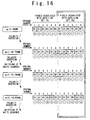
- FIG. 16 is a conceptual diagram showing the polarities of the data signals to be written into the respective pixels and the order of writing the data signals thereinto during respective frames in the second embodiment;
- FIG. 17 is a conceptual diagram showing the polarities of the data signals to be written into the respective pixels and the order of selecting the data lines in a third embodiment
- FIG. 18 is a conceptual diagram showing the polarities of data signals to be written into the respective pixels in the third embodiment
- FIG. 19 is a block diagram showing another exemplary structure of the LCD device that can be employed in the third embodiment.
- FIG. 22 is a conceptual view showing the polarities of the data signals to be written into the respective pixels and the order of writing the data signals thereinto during respective frames in the third embodiment;
- FIG. 23 is a conceptual diagram showing the polarities of the data signals to be written into respective pixels in a fourth embodiment.
- the LCD panel 1 is configured to display images on the basis of the RGB colorimetric system.
- the pixels 13 are each associated with selected one of the “R” (red), “G” (green), and “B” (blue) colors.
- the colors with which the respective pixels 13 are associated are determined such that the pixels 13 positioned in the same column, that is, the pixels coupled to the same data line 12 , are associated with the same color. More specifically, the pixels 13 coupled to the data lines 12 1 , 12 4 , 12 7 , 12 10 , . . . are “R” pixels associated with the red color; the pixels 13 coupled to the data lines 12 2 , 12 5 , 12 8 , 12 11 , . . . are “G” pixels associated with the green color; and the pixels 13 coupled to the data lines 12 3 , 12 6 , 12 9 , 12 12 , . . . are “B” pixels associated with the blue color.
- the R pixels 13 coupled to the data lines 12 1 and 12 7 may be denoted by the reference numeral “ 13 R1 ”, and the R pixels 13 coupled to the data lines 12 4 and 12 10 may be denoted by the reference numeral 13 R2 , if necessary, to thereby clarify the associations between the pixels 13 and the colors.
- the symbol “R” within the subscripts represents the color associated therewith, and the number subsequent to the symbol “R” is used to identify the columns of the pixels 13 .
- the G pixels 13 coupled to data lines 12 2 and 12 8 may be denoted by the reference numeral “ 13 G1 ”, and the G pixels 13 coupled to the data lines 12 5 and 12 11 may be denoted by the reference numeral “ 13 G2 ”.
- the B pixels 13 coupled to the data lines 12 3 and 12 9 may be denoted by the reference numeral 13 B1
- the B pixels 13 coupled to the data lines 12 6 and 12 12 may be denoted by the reference numeral “ 13 B2 ”.
- the pixels 13 each include a TFT 14 and a pixel electrode 15 .
- the TFT 14 has a drain coupled to the associated data line 12 and has a source coupled to the pixel electrode 15 .
- the gate of the TFT 14 is coupled to the associated gate line 11 , so that the TFT 14 provides an electrical connection between the associated data line 12 and the pixel electrode 15 in response to the potential level on the associated gate line 11 .
- the pixels 13 share a common electrode 16 so that the pixel electrode 15 within each pixel 13 opposes the common electrode 16 . Liquid crystal is filled between the pixel electrode 15 and the common electrode 16 , thereby forming a liquid crystal cell.
- the common electrode 16 is coupled to a common-potential generation circuit (not shown), wherein the common electrode 16 is maintained at a predetermined common potential V COM .
- the LCD panel 1 is further provided with input terminals 17 that receive data signals for driving the respective pixels 13 from the controller driver 2 .
- the LCD device 100 is designed to implement time-divisional driving, and therefore the association of the input terminals 17 with the data lines 12 is not a one-to-one association.
- the six data lines 12 associated with the same input terminal 17 is collectively referred to as the data line set 18 .
- the data lines 12 are connected to the associated input terminals 17 through switches 19 that select the data lines 12 to be electrically connected to the associated input terminals 17 . More specifically, the data lines 12 1 to 12 6 are connected to the input terminal 17 1 through the switches 19 1 to 19 6 , respectively, and the data lines connected to the input terminal 17 1 are selectable by using the switches 19 1 to 19 6 , respectively. Correspondingly, the data lines 12 7 to 12 12 are connected to the input the terminal 17 2 through the switches 19 7 to 19 12 , respectively, and the data lines connected to input terminal 17 2 are selectable by using the switches 19 7 to 19 12 .
- the six switches 19 connected to the same input terminal 17 may be collectively referred to as the switch set 20 , hereinafter.
- the switch set 20 1 is composed of the switches 19 1 to 19 6
- the switch set 20 2 is composed of the switches 19 7 to 19 12 .
- a set of six control lines 21 are provided within the LCD panel 1 , which are used to turn on or off the respective switches 19 .
- Each of the switches 19 is connected to any one of six control lines 21 .
- the control lines 21 1 to 21 6 are connected to control input terminals 22 1 to 22 6 , respectively, and receive control signals S 1 to S 6 from the controller driver 2 through the control input terminals 22 1 to 22 6 .
- the switches 19 connected to the control line 21 1 are responsive to the control signal S 1 to be turned on or off, and the switches 19 connected to the control line 21 2 are responsive to the control signal S 2 to be turned on or off. The same goes for the switches 19 connected to the other control lines 21 .
- the connections of the switches 19 to the control lines 21 are different in the adjacent switch sets 20 .
- the leftmost switches 19 1 are connected to the control line 21 1 ;
- the second switch 19 2 from the left is connected to the control line 21 2 ;
- third to sixth switches 19 3 to 19 6 from the left are, respectively, connected to the control lines 21 3 to 21 6 .
- fourth, fifth, and sixth switches 19 10 , 19 11 , and 19 12 from the left are connected to control lines 21 1 , 21 2 , and 21 3 , respectively, and first, second, and third switches 19 7 , 19 8 , and 19 9 from the left are connected to control lines 21 4 , 21 5 , and 21 6 , respectively.
- the difference in the connections of the switches 19 to the control lines 21 in the adjacent switch sets 20 is important to prevent fluctuations in common potential V COM .
- the controller driver 2 is composed of a shift register 31 , an input switch circuitry 32 , a grayscale potential generator 33 , a set of positive-side drive circuits 34 (one shown), a set of negative-side drive circuits 35 (one shown), an output switch circuitry 36 , and a controller circuitry 37 . It should be noted that the positive-side and negative-side drive circuits 34 and 35 must be understood to be alternately arranged in FIG. 5 .
- the shift register 31 is used to temporarily store the pixel data associated with the respective pixels 13 . When the pixels 13 on a specific line are selected, pixel data for the selected pixels 13 are retained in the shift register 31 .
- the input switch circuitry 32 is used to switch the destination of each pixel data stored in the shift register 31 .
- the input switch circuitry 32 transfers pixel data associated with the pixels 13 to be driven with data signals of the positive polarity to the associated positive-side drive circuits 34 , while transferring pixel data associated with the pixels 13 to be driven with data signals of the negative polarity to the associated negative-side drive circuits 35 .
- the grayscale potential generator 33 provides grayscale potential signals, associated with grayscale levels, respectively, for the positive-side drive circuit 34 and the negative-side drive circuit 35 .
- the number of grayscale potential signals being supplied to each of the positive-side drive circuits 34 and the negative-side drive circuits 35 is 2 n , wherein the signal levels of the grayscale potential signals are different from one another.
- the signal levels of the grayscale potential signals supplied to the positive-side drive circuits 34 are all higher than the common potential V COM ; that is, the polarities of the grayscale potential signals supplied to the positive-side drive circuits 34 are all positive.
- the signal levels of the grayscale potential signals supplied to the negative-side drive circuits 34 are all lower than the common potential V COM ; that is, the polarities of the grayscale potential signals supplied to the negative-side drive circuits 34 are all negative.
- the positive-side and negative-side drive circuits 34 and 35 are designed to generate data signals for driving the associated pixels 13 .
- the positive-side drive circuits 34 are used to develop data signals of the positive polarity
- the negative-side drive circuits 35 are used to develop data signals of the negative polarity.
- One positive-side drive circuit 34 and one negative-side drive circuit 35 are provided for every two input terminals 17 of the LCD panel 1 .
- the positive-side drive circuits 34 each include a set of six latches 38 , a selector 39 , a D/A (digital/analog) converter 40 , and an amplifier 41 .
- the latches 38 stores the associated pixel data of the pixels 13 received from the shift register 31 .
- the selector 39 selects one of the associated latches 38 and transfers the pixel data stored in the selected latch to the D/A converter 40 .
- the D/A converter 40 is responsive to the pixel data received from the selector 39 for selecting one of the 2 n grayscale potential signals received from the grayscale potential generator 33 , and outputs the selected grayscale potential signal to the amplifier 41 .
- the polarity of the signal outputted from the D/A converter 40 within the positive-side drive circuit 34 is positive, since the polarity of the selected grayscale potential signal is also positive (defined using the common potential V COM as the reference potential).
- the amplifier 41 is configured of a source follower circuit that provides impedance conversion to thereby develop the data signal for the selected pixel 13 in response to the grayscale potential signal supplied thereto.
- the potential of the data signal developed by the amplifier 41 is substantially identical to the selected grayscale potential signal supplied to the amplifier 41 .
- the negative-side drive circuits 35 substantially have the same configuration as the positive-side drive circuits 34 .
- the difference of the negative-side drive circuits 35 from the positive-side drive circuits 34 is that the polarities of the grayscale potential signals supplied to the D/A converters 40 are negative, and therefore data signals of the negative polarity are developed by the negative-side drive circuits 35 .
- the output switch circuitry 36 switches the destinations of the data signals developed by the positive-side drive circuits 34 and the negative-side drive circuits 35 to thereby output the data signals to the desired ones of the input terminals 17 .
- a data signal outputted from one of the adjacent positive-side and negative-side drive circuits 34 and 35 is supplied to one of the adjacent input terminals 17 1 and 17 2 associated therewith, and another data signal outputted from the other one of the relevant driver circuits 34 and 35 is supplied to the other one of input terminals 17 1 and 17 2 .
- the controller circuitry 37 provides controls for the above-described input switch circuitry 32 , the grayscale potential generator 33 , the positive-side drive circuits 34 , the negative-side drive circuits 35 , and the output switch circuitry 36 . More specifically, the controller circuitry 37 includes an input switch controller 42 , a selector controller 43 , an output switch controller 44 , a time-division switch controller 45 , and a timing controller 46 .
- the input switch controller 42 controls the input switch circuitry 32 , and thereby allows the pixel data contained in the shift register 31 to be transferred to the desired latches 38 .
- the selector controller 43 controls the selectors 39 within the positive-side and negative-side drive circuits 34 and 35 , to thereby transfer the desired pixel data to the D/A converters 40 .
- the output switch controller 44 controls the output switch circuitry 36 to transfer the data signals to the desired input terminals 17 .
- the time-division switch controller 45 generates the control signals S 1 to S 6 to allow the desired switches 19 within the LCD panel 1 to be turned on.
- the timing controller 46 provides timing controls for the input switch controller 42 , the selector controller 43 , the output switch controller 44 , and the time-division switch controller 45 .
- the timing control circuit 46 controls the timing with which the input switch circuitry 32 switches the transfer destinations of the pixel data, the timing with which the selectors 39 switch the pixel data to be transferred to the D/A converters 40 , the timing with which the output switch circuitry 36 switches the destinations of the data signals, and the timing with which the time-division switch control circuit 45 switches the switches 19 to be turned on.
- the structure of the controller driver 2 is not limited to the configuration of FIG. 5 .
- the shift register 31 may be removed from the controller driver 2 .
- the pixel data are supplied to the latches 38 within the positive-side and negative-side drive circuits 34 and 35 through the input switch circuitry 32 .
- level shifters may be additionally provided between the selectors 39 and the D/A converters 40 to enlarge the allowable signal level range of the grayscale potential signals supplied to the D/A converters 40 .
- the level shifters are used to provide signal level matching between the selectors 39 and the D/A converters 40 .
- the operation of the LCD device 10 in this embodiment addresses implementing dot inversion driving and time division driving at the same time, while achieving the stabilization of the common potential V COM .
- data-signal writing into the pixels 13 is performed such that the polarities of data signals to be written into the pixels 13 in odd-numbered columns are opposite to those of data signals to be written into the pixels 13 in even-numbered columns.
- writing the data signals into the pixels 13 is performed such that the polarities of the data signals being written into two arbitrary pixels 13 adjacent to each other in the vertical direction (direction in which the data lines 12 extend) are opposite to each other.
- the polarity of the data signal provided to each pixel is inverted every frame.
- the data lines 12 are serially and time divisionally selected, and the associated data signals are time-divisionally supplied to the desired pixels 13 through the selected data lines 12 .
- the LCD device 10 in this embodiment is designed to develop the data signals to be written into the pixels 13 , so that the data signals applied to the selected data lines 12 include both of positive and negative data signals.
- the LCD device 10 is designed so that the data lines 12 within the adjacent data line sets 18 are selected in different sequences to thereby satisfy the above-mentioned condition. More specifically, as shown in FIG. 7 , the data lines 12 within the data line sets 18 1 are sequentially selected in the order from left to right. This results in that data-signal writing into the pixels 13 associated with the data line sets 18 1 is sequentially performed in to order from the leftmost pixel. For the data line sets 18 2 adjacent to the data line sets 18 1 , on the other hand, the fourth, fifth, and sixth data lines 12 10 , 12 11 , and 12 12 from the left are sequentially selected, and the first, second, and third data lines 12 7 , 12 8 , and 12 9 from the left are then sequentially selected.
- the data signals of the opposite polarities are supplied to the selected data lines 12 , whereby the fluctuation in the common potential V COM is efficiently restrained.
- the pixel row or the pixel line
- the data lines 12 1 coupled to the pixels 13 R1 which are written with the data signals of the positive polarity, are firstly selected.
- the data lines 12 10 coupled to the pixels 13 R2 which are written with the data signals of the negative polarity, are firstly selected.
- This allows the data lines 12 1 and 12 10 to be synchronously supplied with the data signals of the opposite polarity, whereby the level of the current into the common electrode 16 is restrained as shown in FIG. 10 .
- This effectively reduces the fluctuation in the common potential V COM .
- the remaining data lines 12 the data signals of the opposite polarity are supplied to the selected data lines 12 to thereby suppress the fluctuation in the common potential V COM .
- the selection of the data lines 12 in the above-mentioned sequence is automatically accomplished through sequential activation of the control signals S 1 to S 6 , as shown in FIG. 8 .
- This is attributed to the fact that, as shown in FIG. 4 , connections of the switches 19 to the control lines 21 are different between the adjacent switch sets 20 .
- a control signal S 1 is first activated.
- the switches 19 1 and 19 10 are turned on, so that the data lines 12 1 are firstly selected within data line sets 18 1 , and data lines 12 10 are firstly selected within data line sets 18 2 .
- the switches 19 2 and 19 11 are turned on to select the data lines 12 2 and 12 11 .
- the similar procedure is applied to the remaining data lines 12 .
- data-signal writing into the pixels 13 associated with an n-th line is performed in the procedure described in the following.
- data-signal writing into the pixels 13 along the n-th line begins with activating a horizontal synchronizing signal H sync .
- pixel data associated with the pixels 13 on the n-th line is forwarded to the shift register 31 in response to the activation of the horizontal synchronizing signal H sync .
- the pixel data stored in the shift register 31 are then transferred to the latches 38 within the positive-side and negative-side drive circuits 34 and 35 under the control of input switch controller 42 .
- the pixel data associated with the pixels 13 in the odd-numbered columns are transferred to the latches 38 within the positive-side drive circuits 34
- the pixel data associated with the pixels 13 in the even-numbered columns are transferred to the latches 38 within the negative-side drive circuits 35 .
- data signals to be firstly written into the pixels 13 during this writing sequence are generated by the positive-side and negative-side drive circuits 34 and 35 .
- data signals to be written into the pixels 13 coupled to the data lines 12 1 are generated by the associated positive-side drive circuits 34
- data signals to be written into the pixels 13 coupled to the data lines 12 10 are generated by the associated negative-side drive circuits 35 .
- the data-signal generation is performed in detail in a manner described in the following.
- the positive-side drive circuit 34 the pixel data associated with the pixels 13 coupled to the data lines 12 1 are selected by the selectors 39 and then supplied to the D/A converters 40 .
- the D/A converters 40 output the grayscale potential signals associated with the pixel data received from the selectors 39 to the associated amplifiers 41 , and the amplifiers 41 generate the data signals having the desired potentials in response to the selected grayscale potential signals.
- the pixel data for the pixels 13 coupled to the data lines 12 10 are selected by the selectors 39 and are then forwarded to the D/A converters 40 .
- the D/A converters 40 output the grayscale potential signals associated with the pixel data to the associated amplifiers 41 , and the amplifiers 41 generate the data signals having the desired potentials in response to the selected grayscale potential signals.
- the data signals generated by the positive-side drive circuits 34 are output to the input terminals 17 1 under the control of the output switch controller 44 , while the data signals generated by the negative-side drive circuits 35 are output to the input terminals 17 2 . Consequently, as shown in FIG. 7 , the data signals of the positive polarity to be written into the pixels 13 coupled to the data lines 12 1 are supplied to the input terminals 17 1 , and the data signals of the negative polarity to be written into the pixels 13 coupled to the data lines 12 10 are supplied to the input terminals 17 2 .
- the pixels coupled to the data lines 12 2 and 12 11 which are to be secondly driven, are then written with the associated data signals.
- data signals to be written into the pixels 13 coupled to the data lines 12 11 are generated by the positive-side drive circuits 34
- data signals to be written into the pixels 13 coupled to the data lines 12 2 are generated by the negative-side drive circuits 35 .
- the connections of the positive-side and negative-side drive circuits 34 and 35 to the input terminals 17 1 and 17 2 are switched by the output switch circuitry 36 .
- the control signal S 2 is activated to turn on the switches 19 2 connected to the data lines 12 2 and the switches 19 11 connected to the data lines 12 11 . This allows the desired data signals to be written into the pixels 13 coupled to the data lines 12 2 and the pixels 13 coupled to the data lines 12 11 . Data-signal writing into the remaining pixels 13 on the n-th line is then performed in the similar manner.
- Data-signal writing into the pixels 13 on the (n+1)-th line is performed in the same manner, except that the polarities of the data signals are inverted from those of the corresponding data signals associated with the n-th line.
- data signals are written also into the pixels 13 on the remaining lines in the similar manner, with the polarities of the data signal inverted every two columns and every two rows.
- Data-signal writing of one frame is completed through completing data-signal writing into the pixels 13 on all the lines.
- the polarity of the data signal to be written into each pixel 13 is inverted, whereby the frame inversion driving is implemented.
- the voltages developed across the liquid crystal cells within the respective pixels 13 may vary after data-signal writing into the pixels 13 .
- the variations in the voltages across the liquid crystal cells lead to undesirable fluctuations in the grayscale levels of the pixels 13 , and such fluctuations are recognized as uneven brightness by human vision on the LCD panel 1 .
- the difference in the degrees of the voltage variations across the liquid crystal cells between the adjacent pixel columns associated with the same color causes vertical segments of uneven brightness to be recognized as patterns on the LCD panel 1 , the vertical segments extending in the direction along the data lines 12 .
- the difference in the degrees of the voltage variations across the liquid crystal cells of the pixels 13 R1 and 13 R2 both associated with “R”, may cause vertical segments of uneven brightness on the LCD panel 1 .
- the first cause is the leakage through the TFTs within the switches 19 used to select the data lines 12 .
- the data lines 12 have a large length and a large capacitance, so that the TFTs within the switches 19 are required to have high drive capability.
- the TFTs designed to satisfy such requirements are formed to have a large gate width, a short gate length, and a low turn-on resistance; however, the TFTs thus designed inherently suffer large leakage. Consequently, electric charges on the pixel electrodes within the pixels 13 are discharged through the TFTs within the switches 19 , and this causes undesirable variations in the voltages across the pixels 13 .
- the second cause of the voltage variations across the liquid crystal cells is the capacitance coupling between the data lines 12 .
- the potentials on the data lines 12 1 are varied due to the capacitance coupling between the data lines 12 1 and 12 2 , when the data lines 12 2 are driven with the data signals after the data lines 12 1 are placed into the high-impedance state.
- the variations in the potentials on the data lines 12 1 cause fluctuations in the voltages across the pixels 13 R1 coupled thereto.
- the pixels 13 which are earlier written with the data signals experience larger fluctuations in the voltages across the liquid crystal cells.
- the pixels 13 R1 , 13 G1 , 13 B1 , 13 R2 , 13 G2 , and 13 B2 on a certain line associated with a certain data line set 18 are written with data signals in this order, for example, the pixel 13 R1 , which is firstly written with the data signal, experiences the largest variation in the voltage across the liquid crystal cell.
- the order of selecting the data lines 12 that is, the order of writing the data signals into the associated pixels 13 is periodically switched.
- This allows the pixels 13 experiencing increased voltage variations to be temporally and specially scattered, so that the degrees of voltage fluctuations in the liquid crystal cells within the pixels 13 , that is, the degrees of the grayscale level variations can be temporally and specially averaged.
- Averaging the degrees of the grayscale level variations enables reducing the occurrence of uneven brightness, particularly, the generation of vertical segments of uneven brightness.
- the pixels 13 associated with the data line sets 18 1 are driven in this order of the pixels 13 R1 , 13 G1 , 13 B1 , 13 R2 , 13 G2 , and 13 B2 ; whereas the pixels 13 associated with the data line sets 18 2 are driven in this order of the pixels 13 R2 , 13 G2 , 13 B2 , 13 R1 , 13 G1 , and 13 B1 .
- the polarities of the data signals supplied to the respective pixels 13 are inverted.
- the order of writing the data signals into the pixels 13 during the (m+1)-th frame is the same as that during the m-th frame.
- data-signal writing on the data line sets 18 1 is performed in this order of the pixels 13 R2 , 13 G2 , 13 B2 , 13 R1 , 13 G1 , and 13 B1
- data-signal writing for the data line sets 18 2 is performed in this order of the pixels 13 R1 , 13 G1 , 13 B1 , 13 R2 , 13 G2 , and 13 B2 .
- Switching the write sequence is achieved through changing the order of activating the control signals S 1 to S 6 , as shown in FIG. 9 .
- the control signals S 4 to S 6 are sequentially activated, and the control signals S 1 to S 3 are then sequentially activated. Thereby, data-signal writing into the respective pixels 13 is performed in the sequences mentioned above.
- the fact that the order of writing the data signals into the pixels 13 associated with to the same color in the respective data line sets 18 is different between the m-th and (m+2)-th frame is important to reduce the vertical segments of uneven brightness.
- it is now considered about the two R pixels 13 R1 and 13 R2 associated with to a certain data line set 18 1 .
- the pixel 13 R1 is written with the data signal earlier than the pixel 13 R2 during the m-th frame
- the pixel 13 R2 is written with the data signal earlier than the pixel 13 R1 during the (m+2)-th frame. That is, the writing order for the pixels 13 associated with the same red color is different between the m-th and (m+2)-th frame. This is important to temporarily average the grayscale level fluctuations of the pixels 13 associated with the red color and to thereby avoid the generation of the vertical segments of uneven brightness.
- switching the order of writing the data signals into the pixels 13 is effective for avoid the generation of uneven brightness, particularly, the vertical segments of uneven brightness.
- the timing when the order of writing the data signals into the pixels 13 may be modified; the switch timing is arbitrarily selectable during the four-frame cycle.
- the order of writing may be switched at two successive frames, and the order of writing is not changed at the following two frames. It should be noted, however, that the operation shown in FIG. 11 , in which the order of writing the data signals into the pixels 13 is changed every two frames, is preferable to achieve improved temporal uniformity of the grayscale level fluctuations of the respective pixels 13 .
- FIG. 12 is a conceptual diagram showing an exemplary operation of the LCD device 10 in a second embodiment, which depicts the polarities of the data signals to be written into the respective pixels 13 and the order of selecting the data lines 12 .
- the difference from the first embodiment is that the polarities of the data signals written into the pixels 13 are inverted every three columns in the operation in the second embodiment (also see FIG. 13 ); it should be noted that the write operation in the first embodiment involves inverting the polarities of the data signals written into every two pixels 13 adjacent in the horizontal direction (see FIG. 6 ). As shown in FIG.
- the polarities of the data signals written into the respective pixels 13 coupled to the data lines 12 1 to 12 3 are positive within the data line sets 18 1 , while the polarities of the data signals written into the respective pixels 13 coupled to the data lines 12 4 to 12 6 are negative.
- the polarities of the data signals written into the respective pixels 13 coupled to the data lines 12 7 to 12 9 is positive, while the polarities of the data signals written into the respective pixels 13 coupled to data lines 12 10 to 12 12 are negative.
- the order of selecting the data lines 12 in the second embodiment is the identical to that in the first embodiment; the data lines 12 are selected sequentially in the order from the left in data line sets 18 1 . Thereby, data-signal writing into the pixels 13 associated with the data line sets 18 1 is performed sequentially in the order from the leftmost pixel 13 .
- the first, second, and third data lines 12 7 , 12 8 , and 12 9 are selected sequentially in the order from the left, after the fourth, fifth, and sixth data lines 12 10 , 12 11 , and 12 12 are selected sequentially from the left.
- the data signals are sequentially written into the fourth, fifth, and sixth pixels 13 from the left, and the data signals are then sequentially written into the first, second, and third pixels 13 from the left.
- Selecting the data lines 12 in the above-mentioned order is automatically achieved through sequentially activating the control signals S 1 to S 6 in the order shown in FIG. 14 , with the connections between the switches 19 and the control lines 21 designed as shown in FIG. 4 .
- the advantageous feature of the second embodiment is that, as shown in FIG. 14 , the polarities of the data lines 12 to be written into the respective pixels 13 and the order of selecting the data lines 12 are determined so that data signals of the same polarity are successively supplied to the associated input terminals 17 .
- This arrangement is effective to reduce the number of times the data signals to be supplied to the input terminals 17 are inverted, and to reduce the power consumption of the LCD device 10 .
- the data signals are inverted only once on the respective input terminals 17 during one horizontal period.
- the data line sets 18 1 for example, as shown in FIG.
- the data lines 12 1 , 12 2 , and 12 3 coupled to the pixels 13 written with positive data signals are first sequentially selected, and then the data lines 12 4 , 12 5 , and 12 6 coupled to the pixels 13 written with negative data signals are sequentially selected.
- This allows reducing the number of times the data signals to be supplied to the input terminals 17 1 are inverted during each horizontal period down to one, and thereby effectively reduces the power consumption of the LCD device 10 .
- the three columns of the pixels 13 to be written with the data signals of the same polarity each include one column of the pixels 13 associated with the R color, one associated with the G color, and one associated with the B color.
- the pixels 13 to be written with data signal of the positive polarity include pixels 13 R1 associated with the R color, the pixels 13 G1 associated with the G color, and the pixels 13 B1 associated with the B color.
- the pixels 13 to be written with the data signals of the negative polarity include the pixels 13 R2 associated with the R color, the pixels 13 G2 associated with the G color, and the pixels 13 B1 associated with the B color. This arrangement is useful to avoid image quality deterioration.
- the polarities of the data signals written into the respective pixels 13 and the order of selecting the data lines 12 i.e., the order of writing the data signals into the pixels 13 are switched at a cycle of four frames.
- the polarities of the data signals supplied to the respective pixels 13 are inverted every frame, whereas the order of writing the data signals into pixels 13 is switched every two frames.
- writing the data signals into the associated pixels 13 is performed in the manner mentioned below.
- Writing the data signals into the pixels 13 associated with a certain gate line 11 during the m-th frame is performed in the manner mentioned above.
- the polarities of the data signals written into the pixels 13 are inverted every three columns arranged in the horizontal direction.
- Data-signal writing into the pixels 13 associated with the data line sets 18 1 is performed sequentially from the leftmost pixel.
- the fourth, fifth, and sixth pixels 13 are first sequentially written with the data signals from the left, and then the first, second, and third pixels 13 are sequentially written with the data signals from the left.
- the polarities of the data signals supplied to the respective pixels 13 are inverted.
- the order of writing the data signals into the pixels 13 during the (m+1)-th frame is the same as that during the m-th frame.
- the polarities of the data signals supplied to the respective pixel 13 are inverted, while the order of writing the data signals into the pixels 13 is switched within the respective line sets 18 .
- the write sequences for writing the pixels 13 are interchanged between the data line sets 18 1 and 18 2 , to thereby switch the order of data-signal writing.
- the polarities of the data signals supplied to the respective pixels 13 are inverted.
- the order of writing the data signals into the pixels 13 is the same as that in the (m+2)-th frame.
- FIG. 17 is a conceptual diagram illustrating an exemplary operation of the LCD device 10 in a third embodiment, which depicts the polarities of the data signals written into the respective pixels 13 and the order of selecting the data lines 12 .
- the polarities of the data signals written into the pixels 13 are inverted in units of the data line sets 18 , that is, in units of six columns (also see FIG. 18 ). More specifically, the polarities of the data signals written into the pixels 13 associated with the adjacent data line sets 18 are opposite, while the polarities of the data signals to be written into the pixels 13 associated with the same data line sets 18 are the same.
- the polarities of the data signals written into the respective pixels 13 are inverted every pixel rows (or every pixel line). This effectively allows the data signals of opposite polarities to be applied to two data lines 12 respectively selected from the adjacent data line sets 18 , whereby the potential variation on the common electrode 16 is reduced.
- one advantage of the operation of the LCD device 10 in the third embodiment is to eliminate the necessity for inverting the potentials on the respective input terminals 17 in the middle of one horizontal period, and to thereby further reduce the power consumption of the LCD device 10 .
- the polarities of the data signals written into the pixels 13 associated with the data line sets 18 1 are all positive, while the polarities of the data signals written into the pixels 13 associated with the data line sets 18 2 are negative.
- the polarities of all the data signals applied to the data lines 12 associated with the data line sets 18 1 are positive, and the polarities of all the data signals associated with the data line sets 18 2 are negative.
- the potentials on the input terminals 17 1 remain positive, and the potential of the input terminals 17 2 remain negative during the relevant horizontal period, so that the potentials on input terminals 17 1 , 17 2 are not inverted. This allows further reducing the power consumption of LCD device 10 .
- the order of selecting the data lines 12 can be arbitrarily determined in units of the data line sets 18 .
- the data signals of the opposite polarity are applied to the data lines 12 selected regardless of the order of selecting the data lines 12 , because the polarities of the data signals written into the associated pixels 13 are inverted in units of the data line sets 18 .
- the order of selecting the data lines 12 in the adjacent data line sets 18 may be the same.
- the connections between the switches 19 and the control lines 21 are configured to be identical in all the switch sets 20 .
- the switches 19 1 to 19 6 may be connected to the control lines 21 1 to 21 6
- the switches 19 7 to 19 12 may be connected to the control lines 21 1 to 21 6 .
- the data lines 12 are sequentially selected in the order from left to right in both of the data line sets 18 1 and 18 2 , in response to sequential activation of the control signals S 1 to S 6 .
- the polarities of the data signals written into the respective pixels 13 and the order of selecting the data lines 12 i.e., the order of writing the data signals into the associated pixels 13 are switched at a cycle of four frames.
- the polarities of the data signals supplied to the associated pixels 13 are inverted every frame, whereas the order of writing the data signals into the pixels 13 is switched every two frames.
- data-signal writing into the pixels 13 is performed as described in following.
- Data-signal writing into pixels 13 during the m-th frame is performed in the manner mentioned above.
- the polarities of the data signals written into the pixels 13 are inverted in units of the data line sets 18 .
- Data-signal writing into the pixels 13 associated with the data line sets 18 1 and 18 2 is sequentially performed in the order from the leftmost pixel.
- the polarities of the data signals supplied to the respective pixels 13 are inverted.
- the order of for writing the data signals into the associated pixels 13 during the (m+1)-th frame is the same as that during the m-th frame.
- the order of writing the data signals is switched through changing the order of activating the control signals S 1 to S 6 , as shown in FIG. 21 .
- the control signals S 4 to S 6 are sequentially activated, and the control signals S 1 to S 3 are then sequentially activated. This procedure achieves writing the data signals into the respective pixels 13 in the desired order.
- V-line inversion driving vertical inversion driving
- data signals of one polarity are supplied to the pixels 13 in the same column
- data signals of the opposite polarity are supplied to the pixels 13 in the adjacent column.
- the sequence for selection of the data lines 12 is the same that of the first embodiment.
- the use of vertical inversion driving in place of dot inversion driving also satisfies the condition that data signals of the opposite polarities are concurrently applied to the selected data lines 12 for the same reasons as those described in the first embodiment, whereby effectively suppressing the fluctuation in the common potential V COM .
- the use of vertical inversion driving is preferable for effectively reducing the power consumption of the LCD device 10 , and for further stabilizing the common potential V COM .
- the operation in this embodiment may involve switching the polarities of the data signals written into the respective pixel 13 s and the order of writing the data signals into the pixels 13 at the four-frame cycle.
- the polarities of the data signals supplied to the respective pixels 13 are inverted every frame, whereas the order of writing the data signals into the pixels 13 is switched every two frames.
- the LCD device 10 disclosed in any one of the first to fourth embodiments effectively reduces the fluctuations in the common potential V COM (that is the potential on the common electrode 16 ) within the respective pixels 13 even when the number of the data lines 12 to be time-divisionally driven is an even number, through optimization of the polarities of the data signals written into the respective pixels 13 and the order of selecting the data lines 12 .
- the thus-designed architecture provides concurrent implementation of the inversion driving according to the common constant driving and the time-division driving scheme for the LCD device 10 in which the number of data lines 12 to be time-divisionally driven is an even number.
Landscapes
- Engineering & Computer Science (AREA)
- Chemical & Material Sciences (AREA)
- Crystallography & Structural Chemistry (AREA)
- Physics & Mathematics (AREA)
- Computer Hardware Design (AREA)
- General Physics & Mathematics (AREA)
- Theoretical Computer Science (AREA)
- Control Of Indicators Other Than Cathode Ray Tubes (AREA)
- Liquid Crystal (AREA)
- Liquid Crystal Display Device Control (AREA)
Abstract
Description
Claims (21)
Applications Claiming Priority (3)
| Application Number | Priority Date | Filing Date | Title |
|---|---|---|---|
| JP2004165510A JP2005345770A (en) | 2004-06-03 | 2004-06-03 | Liquid crystal panel driving method and liquid crystal display device |
| JP165510/2004 | 2004-06-03 | ||
| JP2004-165510 | 2004-06-03 |
Publications (2)
| Publication Number | Publication Date |
|---|---|
| US20060007213A1 US20060007213A1 (en) | 2006-01-12 |
| US7936326B2 true US7936326B2 (en) | 2011-05-03 |
Family
ID=35498212
Family Applications (1)
| Application Number | Title | Priority Date | Filing Date |
|---|---|---|---|
| US11/142,415 Active 2027-10-30 US7936326B2 (en) | 2004-06-03 | 2005-06-02 | Apparatus and method for LCD panel drive for achieving time-divisional driving and inversion driving |
Country Status (3)
| Country | Link |
|---|---|
| US (1) | US7936326B2 (en) |
| JP (1) | JP2005345770A (en) |
| CN (1) | CN100547641C (en) |
Cited By (3)
| Publication number | Priority date | Publication date | Assignee | Title |
|---|---|---|---|---|
| US20080309599A1 (en) * | 2004-07-21 | 2008-12-18 | Sharp Kabushiki Kaisha | Active Matrix Type Display Device and Drive Control Circuit Used in the Same |
| US20110057949A1 (en) * | 2009-09-08 | 2011-03-10 | Renesas Electronics Corporation | Semiconductor integrated circuit, display device, and display control method |
| US9647004B2 (en) | 2014-09-23 | 2017-05-09 | E Ink Holdings Inc. | Display |
Families Citing this family (11)
| Publication number | Priority date | Publication date | Assignee | Title |
|---|---|---|---|---|
| KR101067618B1 (en) * | 2004-06-29 | 2011-09-27 | 엘지디스플레이 주식회사 | Liquid Crystal Display Panel And Fabricating Method Thereof |
| US20070001965A1 (en) * | 2005-06-30 | 2007-01-04 | Lg.Philips Lcd Co., Ltd. | Driving integrated circuit of liquid crystal display device and driving method thereof |
| JP5089159B2 (en) * | 2006-12-20 | 2012-12-05 | セイコーインスツル株式会社 | Manufacturing method of image sensor IC |
| TWI368213B (en) * | 2007-10-30 | 2012-07-11 | Au Optronics Corp | Liquid crystal display and method for driving same |
| TW200945310A (en) * | 2008-04-29 | 2009-11-01 | Au Optronics Corp | Driving unit |
| TWI480847B (en) * | 2008-05-22 | 2015-04-11 | Au Optronics Corp | Liquid crystal display device and driving method thereof |
| US9083965B2 (en) * | 2009-05-22 | 2015-07-14 | Sharp Kabushiki Kaisha | Stereoscopic display device |
| CN101923261B (en) * | 2010-08-12 | 2012-05-30 | 友达光电股份有限公司 | Liquid crystal display panel |
| TWI416497B (en) * | 2010-12-28 | 2013-11-21 | Au Optronics Corp | Driving method for liquid crystal display device and related device |
| TWI416499B (en) * | 2010-12-30 | 2013-11-21 | Au Optronics Corp | Image displaying method for flat panel display device |
| KR101872993B1 (en) * | 2011-03-28 | 2018-07-03 | 삼성디스플레이 주식회사 | Liquid crystal display |
Citations (7)
| Publication number | Priority date | Publication date | Assignee | Title |
|---|---|---|---|---|
| US5598180A (en) * | 1992-03-05 | 1997-01-28 | Kabushiki Kaisha Toshiba | Active matrix type display apparatus |
| US5648792A (en) * | 1994-03-14 | 1997-07-15 | Hitachi, Ltd. | Liquid crystal display device having a thin film |
| JPH11327518A (en) | 1998-03-19 | 1999-11-26 | Sony Corp | Liquid crystal display device |
| US6049321A (en) * | 1996-09-25 | 2000-04-11 | Kabushiki Kaisha Toshiba | Liquid crystal display |
| JP3056085B2 (en) | 1996-08-20 | 2000-06-26 | 日本電気株式会社 | Drive circuit of matrix type liquid crystal display |
| JP2001166277A (en) * | 1999-12-08 | 2001-06-22 | Mitsubishi Electric Corp | Liquid crystal display device |
| JP3433337B2 (en) | 1995-07-11 | 2003-08-04 | 日本テキサス・インスツルメンツ株式会社 | Signal line drive circuit for liquid crystal display |
-
2004
- 2004-06-03 JP JP2004165510A patent/JP2005345770A/en not_active Withdrawn
-
2005
- 2005-06-02 US US11/142,415 patent/US7936326B2/en active Active
- 2005-06-03 CN CNB2005100760091A patent/CN100547641C/en not_active Expired - Fee Related
Patent Citations (7)
| Publication number | Priority date | Publication date | Assignee | Title |
|---|---|---|---|---|
| US5598180A (en) * | 1992-03-05 | 1997-01-28 | Kabushiki Kaisha Toshiba | Active matrix type display apparatus |
| US5648792A (en) * | 1994-03-14 | 1997-07-15 | Hitachi, Ltd. | Liquid crystal display device having a thin film |
| JP3433337B2 (en) | 1995-07-11 | 2003-08-04 | 日本テキサス・インスツルメンツ株式会社 | Signal line drive circuit for liquid crystal display |
| JP3056085B2 (en) | 1996-08-20 | 2000-06-26 | 日本電気株式会社 | Drive circuit of matrix type liquid crystal display |
| US6049321A (en) * | 1996-09-25 | 2000-04-11 | Kabushiki Kaisha Toshiba | Liquid crystal display |
| JPH11327518A (en) | 1998-03-19 | 1999-11-26 | Sony Corp | Liquid crystal display device |
| JP2001166277A (en) * | 1999-12-08 | 2001-06-22 | Mitsubishi Electric Corp | Liquid crystal display device |
Cited By (4)
| Publication number | Priority date | Publication date | Assignee | Title |
|---|---|---|---|---|
| US20080309599A1 (en) * | 2004-07-21 | 2008-12-18 | Sharp Kabushiki Kaisha | Active Matrix Type Display Device and Drive Control Circuit Used in the Same |
| US8681081B2 (en) * | 2004-07-21 | 2014-03-25 | Sharp Kabushiki Kaisha | Active matrix type display device and drive control circuit used in the same |
| US20110057949A1 (en) * | 2009-09-08 | 2011-03-10 | Renesas Electronics Corporation | Semiconductor integrated circuit, display device, and display control method |
| US9647004B2 (en) | 2014-09-23 | 2017-05-09 | E Ink Holdings Inc. | Display |
Also Published As
| Publication number | Publication date |
|---|---|
| US20060007213A1 (en) | 2006-01-12 |
| CN100547641C (en) | 2009-10-07 |
| CN1705010A (en) | 2005-12-07 |
| JP2005345770A (en) | 2005-12-15 |
Similar Documents
| Publication | Publication Date | Title |
|---|---|---|
| US7936326B2 (en) | Apparatus and method for LCD panel drive for achieving time-divisional driving and inversion driving | |
| KR100843523B1 (en) | A method of operating a liquid crystal display device, a liquid crystal display device, and an lcd panel | |
| CN109817138B (en) | Display screen, display driving device and method for driving sub-pixels on display screen | |
| US7808493B2 (en) | Displaying apparatus using data line driving circuit and data line driving method | |
| US20060028426A1 (en) | LCD apparatus for improved inversion drive | |
| KR100986040B1 (en) | Display driving circuit | |
| US8836629B2 (en) | Image display apparatus and image display method | |
| US6961042B2 (en) | Liquid crystal display | |
| US7649521B2 (en) | Image display apparatus | |
| JP3922736B2 (en) | Liquid crystal display | |
| JP2004279626A (en) | Display device and its driving method | |
| US9196205B2 (en) | Scanning signal line drive circuit and display device equipped with same | |
| JP2011018020A (en) | Display panel driving method, gate driver and display apparatus | |
| KR100561946B1 (en) | Liquid crystal display device and driving method of the same | |
| US20110096062A1 (en) | Liquid crystal display device, driving device for liquid crystal display panel, and liquid crystal display panel | |
| JP2010033038A (en) | Display panel driving method, and display | |
| KR100618509B1 (en) | Driving circuit for a display device | |
| CN100424735C (en) | Method and apparatus for time-divisional display panel drive | |
| US20080180462A1 (en) | Liquid crystal display device and method of driving liquid crystal display device | |
| JP2007179017A (en) | Image display device and method | |
| KR100302829B1 (en) | LCD Electro-optical Device | |
| JP2009134055A (en) | Display device | |
| JPH09258691A (en) | El display device | |
| JP4283172B2 (en) | Liquid crystal electro-optical device | |
| JP3881004B2 (en) | Liquid crystal electro-optical device |
Legal Events
| Date | Code | Title | Description |
|---|---|---|---|
| AS | Assignment |
Owner name: NEC ELECTRONICS CORPORATION, JAPAN Free format text: ASSIGNMENT OF ASSIGNORS INTEREST;ASSIGNORS:HASHIMOTO, YOSHIHARU;KUMETA, MASAYUKI;MATSUURA, KOUJI;REEL/FRAME:016660/0783 Effective date: 20050517 |
|
| AS | Assignment |
Owner name: RENESAS ELECTRONICS CORPORATION, JAPAN Free format text: CHANGE OF NAME;ASSIGNOR:NEC ELECTRONICS CORPORATION;REEL/FRAME:025346/0868 Effective date: 20100401 |
|
| STCF | Information on status: patent grant |
Free format text: PATENTED CASE |
|
| FEPP | Fee payment procedure |
Free format text: PAYOR NUMBER ASSIGNED (ORIGINAL EVENT CODE: ASPN); ENTITY STATUS OF PATENT OWNER: LARGE ENTITY |
|
| FPAY | Fee payment |
Year of fee payment: 4 |
|
| AS | Assignment |
Owner name: RENESAS ELECTRONICS CORPORATION, JAPAN Free format text: CHANGE OF ADDRESS;ASSIGNOR:RENESAS ELECTRONICS CORPORATION;REEL/FRAME:044928/0001 Effective date: 20150806 |
|
| MAFP | Maintenance fee payment |
Free format text: PAYMENT OF MAINTENANCE FEE, 8TH YEAR, LARGE ENTITY (ORIGINAL EVENT CODE: M1552); ENTITY STATUS OF PATENT OWNER: LARGE ENTITY Year of fee payment: 8 |
|
| MAFP | Maintenance fee payment |
Free format text: PAYMENT OF MAINTENANCE FEE, 12TH YEAR, LARGE ENTITY (ORIGINAL EVENT CODE: M1553); ENTITY STATUS OF PATENT OWNER: LARGE ENTITY Year of fee payment: 12 |