US7915958B2 - Amplifier - Google Patents
Amplifier Download PDFInfo
- Publication number
- US7915958B2 US7915958B2 US12/289,520 US28952008A US7915958B2 US 7915958 B2 US7915958 B2 US 7915958B2 US 28952008 A US28952008 A US 28952008A US 7915958 B2 US7915958 B2 US 7915958B2
- Authority
- US
- United States
- Prior art keywords
- transistor
- amplifier
- control
- terminal
- current source
- Prior art date
- Legal status (The legal status is an assumption and is not a legal conclusion. Google has not performed a legal analysis and makes no representation as to the accuracy of the status listed.)
- Expired - Fee Related
Links
Images


Classifications
-
- H—ELECTRICITY
- H03—ELECTRONIC CIRCUITRY
- H03F—AMPLIFIERS
- H03F1/00—Details of amplifiers with only discharge tubes, only semiconductor devices or only unspecified devices as amplifying elements
- H03F1/34—Negative-feedback-circuit arrangements with or without positive feedback
-
- H—ELECTRICITY
- H03—ELECTRONIC CIRCUITRY
- H03F—AMPLIFIERS
- H03F1/00—Details of amplifiers with only discharge tubes, only semiconductor devices or only unspecified devices as amplifying elements
- H03F1/26—Modifications of amplifiers to reduce influence of noise generated by amplifying elements
-
- H—ELECTRICITY
- H03—ELECTRONIC CIRCUITRY
- H03F—AMPLIFIERS
- H03F1/00—Details of amplifiers with only discharge tubes, only semiconductor devices or only unspecified devices as amplifying elements
- H03F1/32—Modifications of amplifiers to reduce non-linear distortion
-
- H—ELECTRICITY
- H03—ELECTRONIC CIRCUITRY
- H03F—AMPLIFIERS
- H03F3/00—Amplifiers with only discharge tubes or only semiconductor devices as amplifying elements
- H03F3/34—DC amplifiers in which all stages are DC-coupled
- H03F3/343—DC amplifiers in which all stages are DC-coupled with semiconductor devices only
-
- H—ELECTRICITY
- H03—ELECTRONIC CIRCUITRY
- H03F—AMPLIFIERS
- H03F2200/00—Indexing scheme relating to amplifiers
- H03F2200/126—A diode being coupled in a feedback path of an amplifier stage, e.g. active or passive diode
-
- H—ELECTRICITY
- H03—ELECTRONIC CIRCUITRY
- H03F—AMPLIFIERS
- H03F2200/00—Indexing scheme relating to amplifiers
- H03F2200/294—Indexing scheme relating to amplifiers the amplifier being a low noise amplifier [LNA]
-
- H—ELECTRICITY
- H03—ELECTRONIC CIRCUITRY
- H03F—AMPLIFIERS
- H03F2200/00—Indexing scheme relating to amplifiers
- H03F2200/372—Noise reduction and elimination in amplifier
-
- H—ELECTRICITY
- H03—ELECTRONIC CIRCUITRY
- H03F—AMPLIFIERS
- H03F2200/00—Indexing scheme relating to amplifiers
- H03F2200/462—Indexing scheme relating to amplifiers the current being sensed
-
- H—ELECTRICITY
- H03—ELECTRONIC CIRCUITRY
- H03F—AMPLIFIERS
- H03F2200/00—Indexing scheme relating to amplifiers
- H03F2200/474—A current mirror being used as sensor
Definitions
- This invention relates to an amplifier and, more particularly, to a low-noise amplifier ideal for use in the receiver of a television set or communications equipment.
- FIG. 3 is a circuit diagram of a preamplifier 40 described in Patent Document 1.
- the preamplifier 40 includes an active element 42 having a base 54 connected to an input terminal 44 of the preamplifier 40 via an input protecting circuit 60 , an emitter 58 connected to a ground terminal 48 via an emitter resistor RE, and a collector 56 connected to a power supply terminal 50 via a collector resistor RL.
- a first feedback loop 64 for feeding back the output of the collector 56 via an emitter follower circuit 70 and a feedback resistor 68 .
- a second feedback loop 66 for feeding back the output of the collector 56 via an inverting amplifier 72 .
- a feedback-type preamplifier referred to as a transimpedance preamplifier for opto-electronic conversion and amplification is described as related art in Patent Document 2.
- a preamplifier having input means for inputting a current signal and amplifying means having transistors for amplifying the input current signal is described.
- This preamplifier includes a control-current source connected to the input means for shunting the input current signal, and current detecting means connected to the interior of the amplifying means, wherein the control-current source is controlled by the current detecting means.
- the control-current source is connected in parallel with the input terminal in order to bypass overcurrent.
- a current mirror circuit with respect to current that flows into an initial-stage transistor of the transimpedance section is constructed by the control-current source and a diode, which is a current detecting means.
- the preamplifier is capable of changing bypass current in accordance with the current waveform of the input signal.
- Patent Documents 1 and 2 are incorporated herein by reference thereto.
- ( 1 ) and ( 2 ) in FIG. 4 indicate the results obtained by simulating a noise (NF) characteristic and distortion (IIP3) characteristic, respectively, with respect to the emitter resistor RE of the transistor 42 .
- IIP3 signifies a third-order intercept point at the input.
- ( 1 ) is the noise characteristic (NF) of the example of the prior art
- ( 2 ) is the distortion (IIP3) characteristic. If the emitter resistor RE is enlarged, the distortion (IIP3) characteristic is improved. However, since the emitter resistor RE will produce thermal noise, the noise characteristic (NF) deteriorates.
- the emitter resistor RE Conversely, if the emitter resistor RE is reduced, the noise characteristic (NF) improves but negative feedback diminishes and the distortion (IIP3) characteristic deteriorates. Further, since the second feedback loop 66 is actuated in order to lower distortion, the emitter resistor RE that gives rise to thermal noise cannot be eliminated. With the conventional preamplifier, therefore, it is difficult to satisfy both of the requirements of low distortion and low noise.
- an amplifier which comprises: an input terminal for inputting an AC voltage signal; and amplifying means having a transistor for amplifying the input AC voltage signal.
- the amplifier further comprises current detecting means connected internally of the amplifying means; and a control-current source controlled by the current detecting means for driving an input stage of the transistor.
- an amplifier which comprises: an input terminal that inputs an AC voltage signal; and an amplifying unit having a transistor for amplifying the input AC voltage signal.
- the amplifier further comprises current detecting unit connected internally of the amplifying unit; and a control-current source controlled by the current detecting unit that drives an input stage of the transistor.
- a signal can be subjected to negative feedback by the current detecting means (unit) without connecting a resistor to the emitter of the transistor, and it is possible to lower both the distortion and noise of the output signal.
- FIG. 1 is a circuit diagram of an amplifier according to a first exemplary embodiment of the present invention
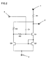
- FIG. 2 is a circuit diagram of an amplifier according to a second exemplary embodiment of the present invention.
- FIG. 3 is a circuit diagram of a preamplifier according to a prior art.
- FIG. 4 shows the distortion characteristic and noise characteristic of the amplifier according to the first exemplary embodiment of the present invention and according to the preamplifier of the prior art.
- An amplifier comprises an input terminal 5 ( FIG. 1 ) for inputting an AC voltage signal; amplifying means (unit) having a transistor Q 1 ( FIG. 1 ) for amplifying the input AC voltage signal; current detecting means Q 2 ( FIG. 1 ) connected internally of the amplifying means (unit); and a control-current source Q 3 ( FIG. 1 ) controlled by the current detecting means (unit) for driving an input stage of the transistor.
- the current detecting means (unit) comprises a diode connected in series with the emitter of the transistor, and the control-current source and diode construct a current mirror circuit.
- the amplifier of the present invention may further comprise a bias supply terminal 4 ( FIG. 1 ) for supplying bias to the transistor; a first resistor element R 2 ( FIG. 1 ) connected between the bias supply terminal and the control-current source; and a second resistor element R 3 ( FIG. 1 ) connected between the base of the transistor and the control-current source.
- the amplifier of the present invention may further comprise a first resistor element R 2 ( FIG. 2 ) connected between the output of the amplifying means (unit) and the control-current source; and a second resistor element R 3 ( FIG. 2 ) connected between the base of the transistor and the control-current source.
- the output of the amplifying means may be the collector of the transistor.
- the transistor may be a field-effect transistor, and the collector, base and emitter may be replaced by a drain, gate and source, respectively.
- the amplifier according to the present invention is so adapted that the output current of the transistor is converted to an AC signal by the current mirror and first resistor element connected to the current mirror, with the voltage signal being subjected to negative feedback.
- FIG. 1 is a circuit diagram of an amplifier according to a first exemplary embodiment of the present invention.
- the amplifier includes a power supply terminal 1 , an output terminal 2 , a ground terminal 3 , a bias supply terminal 4 , an input terminal 5 , a bipolar transistor Q 1 , NMOS transistors Q 2 , Q 3 , resistor elements R 1 , R 2 , R 3 and a capacitance element C 1 .
- the emitter of the bipolar transistor Q 1 , the gate and drain of the NMOS transistor Q 2 and the gate of the NMOS transistor Q 3 are connected.
- the source of the NMOS transistor Q 2 and the source of the NMOS transistor Q 3 are connected to a ground terminal 3 .
- the resistor R 1 is connected between the power supply terminal 1 and the collector of the bipolar transistor Q 1 .
- the resistor R 2 is connected between the bias supply terminal 4 and the drain of the NMOS transistor Q 3
- the resistor R 3 is connected between the drain of the NMOS transistor Q 3 and the base of the bipolar transistor Q 1 .
- the base of the bipolar transistor Q 1 is connected to the input terminal 5 via the capacitance element C 1 , and the collector of the bipolar transistor Q 1 is connected to the output terminal 2 .
- a collector current flows into the bipolar transistor Q 1 in accordance with an AC voltage signal applied to the input terminal 5 , and an output voltage is produced at the output terminal 2 owing to the resistor element R 1 .
- a current proportional to the collector current that flows into the bipolar transistor Q 1 flows into the resistor element R 2 by virtue of the current mirror circuit constructed by the NMOS transistors Q 2 , Q 3 .
- This current is converted to a voltage signal by the resistor element R 2 , and a voltage proportional to the collector current is generated at the drain of the NMOS transistor Q 3 .
- This drain voltage signal flows as negative feedback to the base of the bipolar transistor Q 1 via the resistor element R 3 . Waveform distortion in the amplifier is reduced by this negative feedback.
- the amplifier shown in FIG. 1 is such that a resistor is not connected to the emitter of the bipolar transistor Q 1 , conversion to a voltage signal is made using the current mirror, which comprises the NMOS transistors Q 2 , Q 3 , and the resistor R 2 , and negative feedback is applied. Accordingly, a low-noise characteristic is realized for the amplifier since no use is made of an emitter resistor that causes the noise characteristic to deteriorate.
- plotted points ( 3 ) and ( 4 ) indicate the results obtained by simulating a noise (NF) characteristic and distortion (IIP3) characteristic, respectively, of the amplifier according to the present invention. It will be understood from FIG. 4 that, in contrast with the amplifier of the example of the prior art, both low distortion and low noise can be achieved.
- NF noise
- IIP3 distortion
- FIG. 2 is a circuit diagram of an amplifier according to a second exemplary embodiment of the present invention, in which components identical with those shown in FIG. 1 are designated by like reference characters.
- one end of the resistor element R 2 is connected to the bias supply terminal 4 , as illustrated in FIG. 1
- one end of the resistor element R 2 is connected to the collector of the bipolar transistor Q 1 in the second exemplary embodiment, as illustrated in FIG. 2 .
- the output voltage signal of the bipolar transistor Q 1 is also fed back as negative feedback to the base of the bipolar transistor Q 1 through intervention of the resistor elements R 2 , R 3 .
- the number of negative feedback loops is increased to two, it is easy to design for gain and NF and impedance matching is facilitated.
- the transistor Q 1 is a bipolar transistor
- this transistor may just as well be a field-effect transistor.
- the collector, base and emitter mentioned above would be treated as a drain, gate and source, respectively.
Landscapes
- Engineering & Computer Science (AREA)
- Power Engineering (AREA)
- Physics & Mathematics (AREA)
- Nonlinear Science (AREA)
- Amplifiers (AREA)
Abstract
Description
Claims (17)
Applications Claiming Priority (2)
| Application Number | Priority Date | Filing Date | Title |
|---|---|---|---|
| JP2007-282015 | 2007-10-30 | ||
| JP2007282015A JP2009111724A (en) | 2007-10-30 | 2007-10-30 | Amplifier |
Publications (2)
| Publication Number | Publication Date |
|---|---|
| US20090108940A1 US20090108940A1 (en) | 2009-04-30 |
| US7915958B2 true US7915958B2 (en) | 2011-03-29 |
Family
ID=40048536
Family Applications (1)
| Application Number | Title | Priority Date | Filing Date |
|---|---|---|---|
| US12/289,520 Expired - Fee Related US7915958B2 (en) | 2007-10-30 | 2008-10-29 | Amplifier |
Country Status (4)
| Country | Link |
|---|---|
| US (1) | US7915958B2 (en) |
| EP (1) | EP2056449A3 (en) |
| JP (1) | JP2009111724A (en) |
| KR (1) | KR20090045002A (en) |
Citations (11)
| Publication number | Priority date | Publication date | Assignee | Title |
|---|---|---|---|---|
| US4260955A (en) * | 1979-07-12 | 1981-04-07 | Rca Corporation | Current amplifier with regenerative latch switch |
| DE3035286A1 (en) | 1979-09-21 | 1981-04-09 | Pioneer Electronic Corp., Tokyo | EQUALIZING AMPLIFIER |
| US4626794A (en) * | 1984-04-26 | 1986-12-02 | Kabushiki Kaisha Toshiba | Amplifier circuit using a P channel MOS transistor |
| US5245222A (en) * | 1992-02-28 | 1993-09-14 | Sgs-Thomson Microelectronics, Inc. | Method and apparatus for buffering electrical signals |
| GB2266021A (en) | 1992-04-09 | 1993-10-13 | Pioneer Electronic Corp | Power amplifier with reduced non-linear distortion |
| US5606281A (en) * | 1994-08-25 | 1997-02-25 | U.S. Philips Corporation | Power amplifier stage of the voltage follower type |
| JPH09130157A (en) | 1995-10-27 | 1997-05-16 | Hitachi Ltd | Preamplifier |
| JPH09260974A (en) | 1996-03-26 | 1997-10-03 | Mitsumi Electric Co Ltd | Amplifier circuit |
| US6420931B1 (en) * | 2000-04-06 | 2002-07-16 | National Semiconductor Corporation | High swing output circuit having differential to single-ended conversion and method |
| JP2004024309A (en) | 2002-06-21 | 2004-01-29 | Aloka Co Ltd | Preamplifier for ultrasonic diagnostic equipment |
| US20040141279A1 (en) | 2003-01-21 | 2004-07-22 | Takata Corporation | Initiator and gas generator |
Family Cites Families (2)
| Publication number | Priority date | Publication date | Assignee | Title |
|---|---|---|---|---|
| JPH04369907A (en) * | 1991-06-19 | 1992-12-22 | Hitachi Ltd | High frequency amplifier circuit |
| JP2007282015A (en) | 2006-04-10 | 2007-10-25 | Victor Co Of Japan Ltd | Electroacoustic transducer |
-
2007
- 2007-10-30 JP JP2007282015A patent/JP2009111724A/en active Pending
-
2008
- 2008-10-07 KR KR1020080098021A patent/KR20090045002A/en not_active Ceased
- 2008-10-28 EP EP08018847A patent/EP2056449A3/en not_active Withdrawn
- 2008-10-29 US US12/289,520 patent/US7915958B2/en not_active Expired - Fee Related
Patent Citations (15)
| Publication number | Priority date | Publication date | Assignee | Title |
|---|---|---|---|---|
| US4260955A (en) * | 1979-07-12 | 1981-04-07 | Rca Corporation | Current amplifier with regenerative latch switch |
| DE3035286A1 (en) | 1979-09-21 | 1981-04-09 | Pioneer Electronic Corp., Tokyo | EQUALIZING AMPLIFIER |
| US4356454A (en) | 1979-09-21 | 1982-10-26 | Pioneer Electronic Corporation | Equalizer amplifier |
| US4626794A (en) * | 1984-04-26 | 1986-12-02 | Kabushiki Kaisha Toshiba | Amplifier circuit using a P channel MOS transistor |
| US5245222A (en) * | 1992-02-28 | 1993-09-14 | Sgs-Thomson Microelectronics, Inc. | Method and apparatus for buffering electrical signals |
| US5359295A (en) | 1992-04-09 | 1994-10-25 | Pioneer Electronic Corporation | Power amplifier |
| GB2266021A (en) | 1992-04-09 | 1993-10-13 | Pioneer Electronic Corp | Power amplifier with reduced non-linear distortion |
| US5606281A (en) * | 1994-08-25 | 1997-02-25 | U.S. Philips Corporation | Power amplifier stage of the voltage follower type |
| JPH09130157A (en) | 1995-10-27 | 1997-05-16 | Hitachi Ltd | Preamplifier |
| US5844445A (en) | 1995-10-27 | 1998-12-01 | Hitachi, Ltd. | Feedback type pre-amplifier |
| JPH09260974A (en) | 1996-03-26 | 1997-10-03 | Mitsumi Electric Co Ltd | Amplifier circuit |
| KR100269007B1 (en) | 1996-03-26 | 2000-10-16 | 모리베 이츠오 | Amplification circuit |
| US6420931B1 (en) * | 2000-04-06 | 2002-07-16 | National Semiconductor Corporation | High swing output circuit having differential to single-ended conversion and method |
| JP2004024309A (en) | 2002-06-21 | 2004-01-29 | Aloka Co Ltd | Preamplifier for ultrasonic diagnostic equipment |
| US20040141279A1 (en) | 2003-01-21 | 2004-07-22 | Takata Corporation | Initiator and gas generator |
Non-Patent Citations (1)
| Title |
|---|
| Korean Office Action dated Apr. 27, 2010 (with partial English translation). |
Also Published As
| Publication number | Publication date |
|---|---|
| US20090108940A1 (en) | 2009-04-30 |
| JP2009111724A (en) | 2009-05-21 |
| EP2056449A2 (en) | 2009-05-06 |
| KR20090045002A (en) | 2009-05-07 |
| EP2056449A3 (en) | 2009-05-27 |
Similar Documents
| Publication | Publication Date | Title |
|---|---|---|
| US7944293B2 (en) | Systems and methods for an adaptive bias circuit for a differential power amplifier | |
| KR102027799B1 (en) | Power amplifier circuit | |
| US8106712B2 (en) | Systems and methods for self-mixing adaptive bias circuit for power amplifier | |
| US9641251B1 (en) | Transimpedance amplifier, and related integrated circuit and optical receiver | |
| US6175274B1 (en) | Switched gain low noise amplifier | |
| US7589593B2 (en) | Amplifier circuit having stacked main amplifier and parallel sub-amplifier | |
| US6970044B2 (en) | Audio signal amplifier circuit and electronic apparatus having the same | |
| US7282994B2 (en) | Active load with adjustable common-mode level | |
| US7679452B2 (en) | Amplifier arrangement and method | |
| US7459976B2 (en) | Apparatus and method for biasing cascode devices in a differential pair using the input, output, or other nodes in the circuit | |
| JP6107103B2 (en) | Amplifier and optical receiver | |
| US7439805B1 (en) | Enhancement-depletion Darlington device | |
| US11070176B2 (en) | Amplifier linearization and related apparatus thereof | |
| WO2003092157A1 (en) | Common-base amplifier with high input overload and/or tunable transimpedance | |
| US7915958B2 (en) | Amplifier | |
| US20050007198A1 (en) | Power amplifier module | |
| CN111193477B (en) | Composite amplifier | |
| US7202743B2 (en) | High frequency amplifier | |
| TWI623193B (en) | Power amplifier circuit | |
| CN117650758A (en) | Low noise amplifier and radio frequency chip | |
| US20210297049A1 (en) | Variable gain amplifier and wireless communication device | |
| JP3415986B2 (en) | Optical receiver amplifier | |
| JP2009077142A (en) | Low noise amplifier circuit | |
| US20060033577A1 (en) | Amplifier circuit | |
| JPH0738342A (en) | Preamplifier |
Legal Events
| Date | Code | Title | Description |
|---|---|---|---|
| AS | Assignment |
Owner name: NEC ELECTRONICS CORPORATION, JAPAN Free format text: ASSIGNMENT OF ASSIGNORS INTEREST;ASSIGNOR:OOYABU, HIROKAZU;REEL/FRAME:021827/0795 Effective date: 20081020 |
|
| AS | Assignment |
Owner name: RENESAS ELECTRONICS CORPORATION, JAPAN Free format text: CHANGE OF NAME;ASSIGNOR:NEC ELECTRONICS CORPORATION;REEL/FRAME:025214/0175 Effective date: 20100401 |
|
| STCF | Information on status: patent grant |
Free format text: PATENTED CASE |
|
| FEPP | Fee payment procedure |
Free format text: PAYOR NUMBER ASSIGNED (ORIGINAL EVENT CODE: ASPN); ENTITY STATUS OF PATENT OWNER: LARGE ENTITY |
|
| FPAY | Fee payment |
Year of fee payment: 4 |
|
| AS | Assignment |
Owner name: RENESAS ELECTRONICS CORPORATION, JAPAN Free format text: CHANGE OF ADDRESS;ASSIGNOR:RENESAS ELECTRONICS CORPORATION;REEL/FRAME:044928/0001 Effective date: 20150806 |
|
| FEPP | Fee payment procedure |
Free format text: MAINTENANCE FEE REMINDER MAILED (ORIGINAL EVENT CODE: REM.); ENTITY STATUS OF PATENT OWNER: LARGE ENTITY |
|
| LAPS | Lapse for failure to pay maintenance fees |
Free format text: PATENT EXPIRED FOR FAILURE TO PAY MAINTENANCE FEES (ORIGINAL EVENT CODE: EXP.); ENTITY STATUS OF PATENT OWNER: LARGE ENTITY |
|
| STCH | Information on status: patent discontinuation |
Free format text: PATENT EXPIRED DUE TO NONPAYMENT OF MAINTENANCE FEES UNDER 37 CFR 1.362 |
|
| FP | Lapsed due to failure to pay maintenance fee |
Effective date: 20190329 |