US7911553B2 - Liquid crystal display device - Google Patents
Liquid crystal display device Download PDFInfo
- Publication number
- US7911553B2 US7911553B2 US11/481,863 US48186306A US7911553B2 US 7911553 B2 US7911553 B2 US 7911553B2 US 48186306 A US48186306 A US 48186306A US 7911553 B2 US7911553 B2 US 7911553B2
- Authority
- US
- United States
- Prior art keywords
- liquid crystal
- crystal display
- light emitting
- holder
- support portions
- Prior art date
- Legal status (The legal status is an assumption and is not a legal conclusion. Google has not performed a legal analysis and makes no representation as to the accuracy of the status listed.)
- Active, expires
Links
- 239000004973 liquid crystal related substance Substances 0.000 title claims abstract description 76
- 230000007423 decrease Effects 0.000 claims 1
- 239000000758 substrate Substances 0.000 description 8
- 238000009792 diffusion process Methods 0.000 description 4
- 238000001746 injection moulding Methods 0.000 description 4
- 230000003287 optical effect Effects 0.000 description 4
- 238000000034 method Methods 0.000 description 3
- 229920005989 resin Polymers 0.000 description 3
- 239000011347 resin Substances 0.000 description 3
- 239000003566 sealing material Substances 0.000 description 3
- 239000004820 Pressure-sensitive adhesive Substances 0.000 description 2
- 239000010409 thin film Substances 0.000 description 2
- 239000002390 adhesive tape Substances 0.000 description 1
- 230000000694 effects Effects 0.000 description 1
- 238000012986 modification Methods 0.000 description 1
- 230000004048 modification Effects 0.000 description 1
- 230000002093 peripheral effect Effects 0.000 description 1
- 238000005476 soldering Methods 0.000 description 1
- 229920003002 synthetic resin Polymers 0.000 description 1
- 239000000057 synthetic resin Substances 0.000 description 1
Images


Classifications
-
- G—PHYSICS
- G02—OPTICS
- G02B—OPTICAL ELEMENTS, SYSTEMS OR APPARATUS
- G02B6/00—Light guides; Structural details of arrangements comprising light guides and other optical elements, e.g. couplings
- G02B6/0001—Light guides; Structural details of arrangements comprising light guides and other optical elements, e.g. couplings specially adapted for lighting devices or systems
- G02B6/0011—Light guides; Structural details of arrangements comprising light guides and other optical elements, e.g. couplings specially adapted for lighting devices or systems the light guides being planar or of plate-like form
- G02B6/0081—Mechanical or electrical aspects of the light guide and light source in the lighting device peculiar to the adaptation to planar light guides, e.g. concerning packaging
- G02B6/0086—Positioning aspects
- G02B6/009—Positioning aspects of the light source in the package
-
- G—PHYSICS
- G02—OPTICS
- G02F—OPTICAL DEVICES OR ARRANGEMENTS FOR THE CONTROL OF LIGHT BY MODIFICATION OF THE OPTICAL PROPERTIES OF THE MEDIA OF THE ELEMENTS INVOLVED THEREIN; NON-LINEAR OPTICS; FREQUENCY-CHANGING OF LIGHT; OPTICAL LOGIC ELEMENTS; OPTICAL ANALOGUE/DIGITAL CONVERTERS
- G02F1/00—Devices or arrangements for the control of the intensity, colour, phase, polarisation or direction of light arriving from an independent light source, e.g. switching, gating or modulating; Non-linear optics
- G02F1/01—Devices or arrangements for the control of the intensity, colour, phase, polarisation or direction of light arriving from an independent light source, e.g. switching, gating or modulating; Non-linear optics for the control of the intensity, phase, polarisation or colour
- G02F1/13—Devices or arrangements for the control of the intensity, colour, phase, polarisation or direction of light arriving from an independent light source, e.g. switching, gating or modulating; Non-linear optics for the control of the intensity, phase, polarisation or colour based on liquid crystals, e.g. single liquid crystal display cells
- G02F1/133—Constructional arrangements; Operation of liquid crystal cells; Circuit arrangements
- G02F1/1333—Constructional arrangements; Manufacturing methods
- G02F1/1335—Structural association of cells with optical devices, e.g. polarisers or reflectors
- G02F1/1336—Illuminating devices
- G02F1/133602—Direct backlight
- G02F1/133608—Direct backlight including particular frames or supporting means
-
- G—PHYSICS
- G02—OPTICS
- G02F—OPTICAL DEVICES OR ARRANGEMENTS FOR THE CONTROL OF LIGHT BY MODIFICATION OF THE OPTICAL PROPERTIES OF THE MEDIA OF THE ELEMENTS INVOLVED THEREIN; NON-LINEAR OPTICS; FREQUENCY-CHANGING OF LIGHT; OPTICAL LOGIC ELEMENTS; OPTICAL ANALOGUE/DIGITAL CONVERTERS
- G02F1/00—Devices or arrangements for the control of the intensity, colour, phase, polarisation or direction of light arriving from an independent light source, e.g. switching, gating or modulating; Non-linear optics
- G02F1/01—Devices or arrangements for the control of the intensity, colour, phase, polarisation or direction of light arriving from an independent light source, e.g. switching, gating or modulating; Non-linear optics for the control of the intensity, phase, polarisation or colour
- G02F1/13—Devices or arrangements for the control of the intensity, colour, phase, polarisation or direction of light arriving from an independent light source, e.g. switching, gating or modulating; Non-linear optics for the control of the intensity, phase, polarisation or colour based on liquid crystals, e.g. single liquid crystal display cells
- G02F1/133—Constructional arrangements; Operation of liquid crystal cells; Circuit arrangements
- G02F1/1333—Constructional arrangements; Manufacturing methods
- G02F1/133308—Support structures for LCD panels, e.g. frames or bezels
- G02F1/133317—Intermediate frames, e.g. between backlight housing and front frame
-
- G—PHYSICS
- G02—OPTICS
- G02F—OPTICAL DEVICES OR ARRANGEMENTS FOR THE CONTROL OF LIGHT BY MODIFICATION OF THE OPTICAL PROPERTIES OF THE MEDIA OF THE ELEMENTS INVOLVED THEREIN; NON-LINEAR OPTICS; FREQUENCY-CHANGING OF LIGHT; OPTICAL LOGIC ELEMENTS; OPTICAL ANALOGUE/DIGITAL CONVERTERS
- G02F1/00—Devices or arrangements for the control of the intensity, colour, phase, polarisation or direction of light arriving from an independent light source, e.g. switching, gating or modulating; Non-linear optics
- G02F1/01—Devices or arrangements for the control of the intensity, colour, phase, polarisation or direction of light arriving from an independent light source, e.g. switching, gating or modulating; Non-linear optics for the control of the intensity, phase, polarisation or colour
- G02F1/13—Devices or arrangements for the control of the intensity, colour, phase, polarisation or direction of light arriving from an independent light source, e.g. switching, gating or modulating; Non-linear optics for the control of the intensity, phase, polarisation or colour based on liquid crystals, e.g. single liquid crystal display cells
- G02F1/133—Constructional arrangements; Operation of liquid crystal cells; Circuit arrangements
- G02F1/1333—Constructional arrangements; Manufacturing methods
- G02F1/1335—Structural association of cells with optical devices, e.g. polarisers or reflectors
- G02F1/1336—Illuminating devices
- G02F1/133602—Direct backlight
- G02F1/133603—Direct backlight with LEDs
-
- G—PHYSICS
- G02—OPTICS
- G02F—OPTICAL DEVICES OR ARRANGEMENTS FOR THE CONTROL OF LIGHT BY MODIFICATION OF THE OPTICAL PROPERTIES OF THE MEDIA OF THE ELEMENTS INVOLVED THEREIN; NON-LINEAR OPTICS; FREQUENCY-CHANGING OF LIGHT; OPTICAL LOGIC ELEMENTS; OPTICAL ANALOGUE/DIGITAL CONVERTERS
- G02F1/00—Devices or arrangements for the control of the intensity, colour, phase, polarisation or direction of light arriving from an independent light source, e.g. switching, gating or modulating; Non-linear optics
- G02F1/01—Devices or arrangements for the control of the intensity, colour, phase, polarisation or direction of light arriving from an independent light source, e.g. switching, gating or modulating; Non-linear optics for the control of the intensity, phase, polarisation or colour
- G02F1/13—Devices or arrangements for the control of the intensity, colour, phase, polarisation or direction of light arriving from an independent light source, e.g. switching, gating or modulating; Non-linear optics for the control of the intensity, phase, polarisation or colour based on liquid crystals, e.g. single liquid crystal display cells
- G02F1/133—Constructional arrangements; Operation of liquid crystal cells; Circuit arrangements
- G02F1/1333—Constructional arrangements; Manufacturing methods
- G02F1/1335—Structural association of cells with optical devices, e.g. polarisers or reflectors
- G02F1/1336—Illuminating devices
- G02F1/133615—Edge-illuminating devices, i.e. illuminating from the side
Definitions
- the present invention relates to a liquid crystal display device, and more particularly to a technique which is effectively applicable to a backlight which houses light emitting elements such as white light emitting diodes (LED) therein.
- LED white light emitting diodes
- a TFT (Thin Film Transistor) type liquid crystal display module having a miniaturized liquid crystal panel which is capable of performing a color display with the number of sub color pixels of approximately 240 ⁇ 320 ⁇ 3 has been popularly used as a display part of a portable equipment such as a mobile phone.
- a liquid crystal display module includes a liquid crystal display panel and a backlight which radiates light to the liquid crystal display panel.
- the liquid crystal display module which is used as a display part of a portable equipment such as a mobile phone uses, for example, white light emitting diodes as a light source of the backlight.
- the white light emitting diodes are mounted in the inside of a holder which constitutes a component of the backlight.
- the contact between the holder and the white light emitting diodes of the backlight invites not only physical rupture of the white light emitting diodes but also a drawback that a light guide plate and the white light emitting diodes which constitute components of the backlight are offset from each other thus degenerating the brightness property.
- the present invention has been made to overcome these drawbacks of the above-mentioned prior art and it is an object of the present invention to provide a technique which can reduce a thickness of a liquid crystal display device while preventing a holder and a light emitting element of a backlight from coming into contact with each other.
- a liquid crystal display device includes a backlight and a liquid crystal display panel which is arranged above the backlight, wherein the backlight includes a frame-like holder and a light emitting element which is housed in the inside of the holder, the holder includes support portions which support the liquid crystal display panel, the light emitting elements are housed in the inside of the holder at the support portion on a side opposite to the liquid crystal display panel, and the support portion includes recessed portions which are formed on a side opposite to a side which supports the liquid crystal display panel and at positions which face the light emitting element in an opposed manner.
- the light emitting element is formed of a white light emitting diode and a distal end portion of the light emitting element on a side which faces the support portion in an opposed manner is positioned in the inside of the recessed portion.
- the light emitting element is mounted on a flexible printed wiring board, and the flexible printed wiring board is fixed to a frame portion of the holder.
- the liquid crystal display device of the present invention it is possible to reduce the thickness of the liquid crystal display device while preventing the holder and the light emitting element of the backlight from coming into contact with each other.
- FIG. 1 is a cross-sectional view showing the cross-sectional structure in the vicinity of a white light emitting diode which constitutes a light emitting element in a liquid crystal display module of this embodiment of the present invention
- FIG. 2A to FIG. 2C are views for explaining a shape of a holder shown in FIG. 1 ;
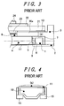
- FIG. 3 is a cross-sectional view showing a cross-sectional structure in the vicinity of a white light emitting diode in a conventional liquid crystal display module;
- FIG. 4 is a view showing details of the white light emitting diode 1 ;
- FIG. 5 is a cross-sectional view showing the cross-sectional structure in the vicinity of a white light emitting diode in a conventional liquid crystal display module when a profile size of the white light emitting diode 1 is increased.
- the liquid crystal display module of the embodiment of the present invention is a TFT type liquid crystal display module having a miniaturized liquid crystal panel which is capable of a color display with the number of sub pixels of approximately 240 ⁇ 320 ⁇ 3 and is used as a display part of a portable equipment such as a mobile phone.
- the liquid crystal display module of the present embodiment is constituted of a backlight and a liquid crystal display panel which is arranged above the backlight.
- FIG. 1 is a cross-sectional view showing the cross-sectional structure of the liquid crystal display module of the present invention in the vicinity of a white light emitting diode which constitutes the light emitting element.
- numeral 1 indicates white light emitting diodes
- numeral 2 indicates a flexible printed wiring board (FPC)
- numeral 3 indicates a holder
- numeral 4 indicates a light guide plate
- numeral 5 indicates an incident surface of the light guide plate 4
- numeral 6 indicates a light emitting surface of the white light emitting diode 1
- numeral 7 indicates a clearance
- numeral 8 indicates a group of optical sheets (a lower diffusion sheet, a pair of lens sheets, an upper diffusion sheet)
- numeral 13 indicates a pressure sensitive adhesive double coated tape
- numeral 17 indicates a reflection sheet
- numeral 21 indicates a TFT substrate
- numeral 22 indicates a counter substrate
- numerals 23 , 24 indicate polarizers.
- the liquid crystal display panel is constituted in a state that the TFT substrate 21 on which pixel electrodes, thin film transistors and the like are mounted and the counter substrate 22 on which color filters and the like are formed are overlapped to each other with a predetermined gap therebetween and both substrates are laminated to each other using a sealing material which is provided in a frame shape in the vicinity of a peripheral portion between both substrates, and a liquid crystal is filled in the inside of the sealing material arranged between both substrates via a liquid crystal filling port which is formed in a portion of the sealing material and sealed and, further, the polarizers ( 23 , 24 ) are adhered to the outer sides of both substrates.
- the present invention does not relate to the inner structure of the liquid crystal panel and hence, the detailed explanation of the inner structure of the liquid crystal panel is omitted. Further, the present invention is applicable to the liquid crystal panel having any structure.
- the backlight of this embodiment includes the group of the optical sheets 8 which is constituted of the lower diffusion sheet, two lens sheets and an upper diffusion sheet, the light guide plate 4 , a reflection sheet 17 which is arranged below the light guide plate 4 , the white light emitting diodes 1 which are arranged on a side surface of the light guide plate 4 .
- the backlight of this embodiment is constituted in a state that the group of the optical sheets 8 , the light guide plate 4 , the reflection sheet 17 and the white light emitting diodes 1 are arranged in the inside of the holder 3 in order as shown in FIG. 1 .
- FIG. 2A to FIG. 2C are views for explaining a shape of the holder shown in FIG. 1 .
- FIG. 2A is a view of the holder shown in FIG. 1 as viewed from the above (the liquid crystal display panel side)
- FIG. 2B is a view of the holder shown in FIG. 1 as viewed from below (the light guide plate side)
- FIG. 2C is a cross-sectional view taken along a A-A′ in FIG. 2A .
- numeral 16 indicates an opening portion and numerals 30 a , 30 b indicate support portions.
- the holder 3 of this embodiment is a frame-like body (or a cylindrical body) having a rectangular cross-sectional shape and the support portions ( 30 a , 30 b ) which support the liquid crystal display panel are formed therein while forming the opening portion 16 .
- the liquid crystal display panel is fixed to the support portions ( 30 a , 30 b ) of the holder 3 by using the pressure sensitive adhesive double coated tape 13 . Further, the white light emitting diodes 1 are mounted on the flexible printed wiring board 2 and are arranged in a state that the incident surface 5 of the light guide plate 4 which is arranged in the inside of the holder 3 and the light emitting surfaces 6 of the white light emitting diodes 1 are aligned with each other.
- the flexible printed wiring board 2 is fixed to the holder 3 using an adhesive tape or the like.
- This embodiment is characterized in that in the support portion 30 a of the holder 3 , recessed portions 12 each of which is made as small as possible while having a size set larger than a maximum profile size which the white light emitting diode 1 can assume (a maximum profile size which the white light emitting diode 1 can assume as viewed from the liquid crystal display panel side) are formed.
- FIG. 3 is a cross-sectional view showing the cross-sectional structure of a conventional liquid crystal display module in the vicinity of a white light emitting diode.
- a white light emitting diode land a light guide plate 4 are arranged in the inside of a holder 3 in a state that the center of a light emitting surface 6 of the white light emitting diode 1 and the center of an incident surface 5 of the light guide plate 4 are aligned with each other and, further, a clearance 7 is formed between the white light emitting diode 1 and the holder 3 thus preventing the white light emitting diode 1 and the holder 3 from coming into contact with each other.
- the thickness of the liquid crystal display module When the thickness of the liquid crystal display module is to be reduced, it is necessary to reduce respective thicknesses of the white light emitting diodes 1 , the light guide plate 4 and the group of optical sheets 8 and, at the same time, it is also necessary to reduce a thickness (“a” shown in FIG. 3 ) of a support portion ( 30 a , 30 b ) of the holder 3 . It is further necessary to minimize the clearance 7 to reduce the thickness of the liquid crystal display module.
- the detail of the white light emitting diode 1 is shown in FIG. 4 .
- the white light emitting diode 1 is configured such that a light emitting portion 10 is covered with a resin separator 11 .
- numerals 15 indicate electrodes.
- a the separator 11 made of resin is thermally expanded and this thermal expansion of the separator 11 may cause the permanent deformation of the separator 11 thus increasing a profile size of the white light emitting diode 1 which exhibits a shape shown in FIG. 4( b ).
- FIG. 5 is a cross-sectional view showing the cross-sectional structure in the vicinity of the white light emitting diode when the profile size of the white light emitting diode 1 is increased in the conventional liquid crystal display module.
- the white light emitting diode 1 assumes a shape which projects from the holder 3 and hence, when an external pressure is applied to the white light emitting diode 1 in the direction indicated by an arrow (d) in FIG. 5 , the white light emitting diode 1 is pressed between the external pressure and the holder 3 and hence, in a worst case, the white light emitting diode 1 may be broken.
- the center of the light emitting surface 6 of the white light emitting diode 1 is offset from the center of the incident surface 5 of the light guide plate 4 . Accordingly, a portion of light 9 which is emitted from the white light emitting diode 1 does not enter the incident surface 5 of the light guide plate 4 and is emitted to the outside of the light guide plate 4 and hence, the brightness of the backlight is lowered.
- the holder 3 is formed of a synthetic resin by injection molding.
- a thickness (“a” shown in FIG. 3 ) of the support portion ( 30 a , 30 b ) of the holder 3 shown in FIG. 3 .
- the resin does not reach a portion of the holder 3 which has a reduced thickness and hence, a shrinkage cavity which causes a non-uniform thickness is generated.
- the recessed portions 12 which are made as small as possible while having the size set larger than a maximum profile size which the white light emitting diodes 1 can assume are formed.
- the recessed portions 12 are formed at positions where the recessed portions 12 face the white light emitting diodes 1 .
- a distal end portion of the white light emitting diode 1 on a side which faces the support portion 30 a in an opposed manner is housed in the inside of the recessed portion 12 which is formed in the holder 3 and, as a result, the white light emitting diode 1 is not brought into contact with the holder 3 as described above and the rupture of the white light emitting diode 1 and lowering of the brightness of the backlight can be prevented.
- the present invention is not limited to the constitution in which the flexible printed wiring board 2 on which the white light emitting diodes 1 are mounted is fixed to the holder 3 .
- the present invention is applicable to other constitutions for arranging the white light emitting diodes 1 in the inside of the holder 3 such as the constitution in which a flexible printed circuit board 2 on which white light emitting diodes 1 are mounted is fixed to a housing not shown in the drawing which accommodates a backlight or the constitution in which a flexible printed circuit board 2 on which white light emitting diodes 1 are mounted is sandwiched between a bottom surface of a housing not shown in the drawing and the holder 3 .
- the present invention is not limited to the constitution which uses the white light emitting diodes as the light source of the backlight and the present invention is also applicable to the constitution which uses light emitting diodes having another color or other light emitting elements.
Abstract
Description
Claims (14)
Applications Claiming Priority (2)
| Application Number | Priority Date | Filing Date | Title |
|---|---|---|---|
| JP2005199033A JP4679985B2 (en) | 2005-07-07 | 2005-07-07 | Liquid crystal display device |
| JP2005-199033 | 2005-07-07 |
Publications (2)
| Publication Number | Publication Date |
|---|---|
| US20070008451A1 US20070008451A1 (en) | 2007-01-11 |
| US7911553B2 true US7911553B2 (en) | 2011-03-22 |
Family
ID=37597379
Family Applications (1)
| Application Number | Title | Priority Date | Filing Date |
|---|---|---|---|
| US11/481,863 Active 2027-03-30 US7911553B2 (en) | 2005-07-07 | 2006-07-07 | Liquid crystal display device |
Country Status (3)
| Country | Link |
|---|---|
| US (1) | US7911553B2 (en) |
| JP (1) | JP4679985B2 (en) |
| CN (1) | CN1892360B (en) |
Cited By (9)
| Publication number | Priority date | Publication date | Assignee | Title |
|---|---|---|---|---|
| US20090296423A1 (en) * | 2008-06-02 | 2009-12-03 | Hwan-Jin Kim | Backlight assembly and display device having the same |
| US20110014955A1 (en) * | 2009-07-20 | 2011-01-20 | Sang Joon Kim | Mobile terminal having an led backlight unit |
| US20110141670A1 (en) * | 2009-12-16 | 2011-06-16 | Samsung Electronics Co., Ltd. | Backlight unit and display apparatus having the same |
| US20130083267A1 (en) * | 2011-09-14 | 2013-04-04 | Ge-Ge Zhou | Assembling method and structure for liquid crystal display device, liquid crystal panel and backlight module |
| US9798189B2 (en) | 2010-06-22 | 2017-10-24 | Toyobo Co., Ltd. | Liquid crystal display device, polarizer and protective film |
| US10054816B2 (en) | 2009-11-12 | 2018-08-21 | Toyo Boseki Kabushiki Kaisha | Method for improving visibility of liquid crystal display device, and liquid crystal display device using same |
| US10175494B2 (en) | 2011-05-18 | 2019-01-08 | Toyobo Co., Ltd. | Polarizing plate suitable for liquid crystal display device capable of displaying three-dimensional images, and liquid crystal display device |
| US10180597B2 (en) | 2011-05-18 | 2019-01-15 | Toyobo Co., Ltd. | Liquid crystal display device, polarizing plate, and polarizer protection film |
| US10823909B2 (en) | 2018-10-30 | 2020-11-03 | Samsung Electronics Co., Ltd. | Display apparatus |
Families Citing this family (15)
| Publication number | Priority date | Publication date | Assignee | Title |
|---|---|---|---|---|
| KR101348247B1 (en) * | 2007-06-07 | 2014-01-09 | 삼성디스플레이 주식회사 | Liquid crystal display device |
| JP2009216753A (en) * | 2008-03-07 | 2009-09-24 | Hitachi Displays Ltd | Liquid crystal display device |
| CN103207466B (en) * | 2008-03-28 | 2016-01-06 | 北京京东方光电科技有限公司 | Framework and liquid crystal indicator |
| CN101546057B (en) * | 2008-03-28 | 2013-05-08 | 北京京东方光电科技有限公司 | Frame and liquid crystal display device |
| WO2010023996A1 (en) * | 2008-08-29 | 2010-03-04 | シャープ株式会社 | Backlight device and display device provided with the same |
| JP5257010B2 (en) | 2008-11-14 | 2013-08-07 | セイコーエプソン株式会社 | Electro-optical device and electronic apparatus |
| TWI384281B (en) * | 2009-03-27 | 2013-02-01 | Au Optronics Corp | Display apparatus and manufacturing method thereof |
| JP5436935B2 (en) * | 2009-05-28 | 2014-03-05 | 株式会社ジャパンディスプレイ | Liquid crystal display |
| US8777471B2 (en) | 2011-03-08 | 2014-07-15 | Omron Corporation | Electronic equipment provided with display portion |
| JP5348158B2 (en) * | 2011-03-08 | 2013-11-20 | オムロン株式会社 | Electronic device with display |
| CN202253135U (en) * | 2011-08-05 | 2012-05-30 | 深圳市华星光电技术有限公司 | Backlight module and liquid crystal display (LCD) |
| US8582050B2 (en) | 2011-08-05 | 2013-11-12 | Shenzhen China Star Optoelectronics Technology Co., Ltd. | Backlight module and liquid crystal display |
| CN102401334B (en) * | 2011-11-18 | 2013-11-27 | 深圳市华星光电技术有限公司 | Back frame of flat panel display device and backlight system |
| CN104214590A (en) * | 2013-05-30 | 2014-12-17 | 北京京东方光电科技有限公司 | Backlight module and liquid crystal display device |
| KR20150038876A (en) * | 2013-10-01 | 2015-04-09 | 삼성디스플레이 주식회사 | Liquid crystal display apparatus |
Citations (14)
| Publication number | Priority date | Publication date | Assignee | Title |
|---|---|---|---|---|
| US5453855A (en) * | 1992-12-15 | 1995-09-26 | Koito Manufacturing Co., Ltd. | Liquid crystal display device backlit by LED's coupled to printed circuit board |
| JPH1022665A (en) * | 1996-07-02 | 1998-01-23 | Oki Electric Ind Co Ltd | Lcd module structure of lcd display |
| US5729310A (en) * | 1995-11-20 | 1998-03-17 | Sharp Kabushiki Kaisha | Lighting apparatus |
| US20020015005A1 (en) | 2000-06-13 | 2002-02-07 | Chiaki Imaeda | Electro-optical device, method for manufacturing electro-optical device, light guide, liquid crystal device, method for manufacturing liquid crystal device, and electronic equipment |
| US20040008512A1 (en) * | 2002-07-11 | 2004-01-15 | Yong-Il Kim | Backlight assembly and liquid crystal display apparatus having the same |
| US6885411B2 (en) * | 2000-07-05 | 2005-04-26 | Hitachi, Ltd. | Liquid crystal display monitor having an improved structure for mounting a liquid crystal display module |
| US20050099556A1 (en) | 2002-09-25 | 2005-05-12 | Kazuya Shimojoh | Backlight unit and liquid crystal display apparatus |
| US6910784B2 (en) * | 2002-03-25 | 2005-06-28 | Advanced Display Inc. | Panel light source device and fabrication process for the same |
| JP2005183536A (en) | 2003-12-17 | 2005-07-07 | Seiko Epson Corp | Flexible wiring board, electro-optical device, and electronic apparatus |
| US7113235B2 (en) * | 2002-03-25 | 2006-09-26 | Kabushiki Kaisha Toshiba | Liquid crystal display device |
| US7298432B2 (en) * | 2002-05-24 | 2007-11-20 | Samsung Electronics Co., Ltd. | Liquid crystal display apparatus |
| US7344291B2 (en) * | 2003-12-15 | 2008-03-18 | Sony Corporation | Illuminating device and backlight device employing the illuminating device |
| US7585099B2 (en) * | 2004-04-30 | 2009-09-08 | Lg Display Co., Ltd. | Backlight unit and liquid crystal display device using the same |
| US7742121B2 (en) * | 2003-10-28 | 2010-06-22 | Mitsubishi Denki Kabushiki Kaisha | Liquid crystal display apparatus and electronic equipment |
Family Cites Families (1)
| Publication number | Priority date | Publication date | Assignee | Title |
|---|---|---|---|---|
| WO2005000139A1 (en) * | 2003-04-28 | 2005-01-06 | Bracco Imaging Spa | Surgical navigation imaging system |
-
2005
- 2005-07-07 JP JP2005199033A patent/JP4679985B2/en active Active
-
2006
- 2006-06-29 CN CN2006100959818A patent/CN1892360B/en active Active
- 2006-07-07 US US11/481,863 patent/US7911553B2/en active Active
Patent Citations (14)
| Publication number | Priority date | Publication date | Assignee | Title |
|---|---|---|---|---|
| US5453855A (en) * | 1992-12-15 | 1995-09-26 | Koito Manufacturing Co., Ltd. | Liquid crystal display device backlit by LED's coupled to printed circuit board |
| US5729310A (en) * | 1995-11-20 | 1998-03-17 | Sharp Kabushiki Kaisha | Lighting apparatus |
| JPH1022665A (en) * | 1996-07-02 | 1998-01-23 | Oki Electric Ind Co Ltd | Lcd module structure of lcd display |
| US20020015005A1 (en) | 2000-06-13 | 2002-02-07 | Chiaki Imaeda | Electro-optical device, method for manufacturing electro-optical device, light guide, liquid crystal device, method for manufacturing liquid crystal device, and electronic equipment |
| US6885411B2 (en) * | 2000-07-05 | 2005-04-26 | Hitachi, Ltd. | Liquid crystal display monitor having an improved structure for mounting a liquid crystal display module |
| US7113235B2 (en) * | 2002-03-25 | 2006-09-26 | Kabushiki Kaisha Toshiba | Liquid crystal display device |
| US6910784B2 (en) * | 2002-03-25 | 2005-06-28 | Advanced Display Inc. | Panel light source device and fabrication process for the same |
| US7298432B2 (en) * | 2002-05-24 | 2007-11-20 | Samsung Electronics Co., Ltd. | Liquid crystal display apparatus |
| US20040008512A1 (en) * | 2002-07-11 | 2004-01-15 | Yong-Il Kim | Backlight assembly and liquid crystal display apparatus having the same |
| US20050099556A1 (en) | 2002-09-25 | 2005-05-12 | Kazuya Shimojoh | Backlight unit and liquid crystal display apparatus |
| US7742121B2 (en) * | 2003-10-28 | 2010-06-22 | Mitsubishi Denki Kabushiki Kaisha | Liquid crystal display apparatus and electronic equipment |
| US7344291B2 (en) * | 2003-12-15 | 2008-03-18 | Sony Corporation | Illuminating device and backlight device employing the illuminating device |
| JP2005183536A (en) | 2003-12-17 | 2005-07-07 | Seiko Epson Corp | Flexible wiring board, electro-optical device, and electronic apparatus |
| US7585099B2 (en) * | 2004-04-30 | 2009-09-08 | Lg Display Co., Ltd. | Backlight unit and liquid crystal display device using the same |
Cited By (14)
| Publication number | Priority date | Publication date | Assignee | Title |
|---|---|---|---|---|
| US8403548B2 (en) * | 2008-06-02 | 2013-03-26 | Samsung Display Co., Ltd. | Backlight assembly and display device having the same |
| US20090296423A1 (en) * | 2008-06-02 | 2009-12-03 | Hwan-Jin Kim | Backlight assembly and display device having the same |
| US20110014955A1 (en) * | 2009-07-20 | 2011-01-20 | Sang Joon Kim | Mobile terminal having an led backlight unit |
| US8224391B2 (en) * | 2009-07-20 | 2012-07-17 | Lg Electronics Inc. | Mobile terminal having an LED backlight unit |
| US10054816B2 (en) | 2009-11-12 | 2018-08-21 | Toyo Boseki Kabushiki Kaisha | Method for improving visibility of liquid crystal display device, and liquid crystal display device using same |
| US10948764B2 (en) | 2009-11-12 | 2021-03-16 | Keio University | Method for improving visibility of liquid crystal display device, and liquid crystal display device using the same |
| US20110141670A1 (en) * | 2009-12-16 | 2011-06-16 | Samsung Electronics Co., Ltd. | Backlight unit and display apparatus having the same |
| US9798189B2 (en) | 2010-06-22 | 2017-10-24 | Toyobo Co., Ltd. | Liquid crystal display device, polarizer and protective film |
| US9897857B2 (en) | 2010-06-22 | 2018-02-20 | Toyobo Co., Ltd. | Liquid crystal display device, polarizer and protective film |
| US10503016B2 (en) | 2010-06-22 | 2019-12-10 | Toyobo Co., Ltd. | Liquid crystal display device, polarizer and protective film |
| US10175494B2 (en) | 2011-05-18 | 2019-01-08 | Toyobo Co., Ltd. | Polarizing plate suitable for liquid crystal display device capable of displaying three-dimensional images, and liquid crystal display device |
| US10180597B2 (en) | 2011-05-18 | 2019-01-15 | Toyobo Co., Ltd. | Liquid crystal display device, polarizing plate, and polarizer protection film |
| US20130083267A1 (en) * | 2011-09-14 | 2013-04-04 | Ge-Ge Zhou | Assembling method and structure for liquid crystal display device, liquid crystal panel and backlight module |
| US10823909B2 (en) | 2018-10-30 | 2020-11-03 | Samsung Electronics Co., Ltd. | Display apparatus |
Also Published As
| Publication number | Publication date |
|---|---|
| CN1892360B (en) | 2010-12-01 |
| US20070008451A1 (en) | 2007-01-11 |
| CN1892360A (en) | 2007-01-10 |
| JP4679985B2 (en) | 2011-05-11 |
| JP2007017696A (en) | 2007-01-25 |
Similar Documents
| Publication | Publication Date | Title |
|---|---|---|
| US7911553B2 (en) | Liquid crystal display device | |
| US20100020261A1 (en) | Liquid crystal display device | |
| US7463325B2 (en) | Liquid crystal display device | |
| JP4244942B2 (en) | Liquid crystal device, lighting device, and electronic device | |
| US20070019127A1 (en) | Liquid crystal display device | |
| US10180534B2 (en) | Borderless display device including display module | |
| JP5436935B2 (en) | Liquid crystal display | |
| US20070252922A1 (en) | Liquid crystal display device | |
| US8379163B2 (en) | Display device | |
| US20070229726A1 (en) | Liquid crystal display device | |
| JP5255960B2 (en) | Liquid crystal display | |
| US7714953B2 (en) | Display device | |
| KR950033579A (en) | LCD and information processing device | |
| JP2008197125A (en) | Liquid crystal display device | |
| US9980387B2 (en) | Flexible printed circuit board and display device including the same | |
| CN106842694B (en) | Backlight unit and display device including the same | |
| US9110323B2 (en) | Liquid crystal display device | |
| KR102209414B1 (en) | Liquid crystal display device module | |
| JP2005077755A (en) | Frame case | |
| JP2007256586A (en) | Display device and electronic apparatus | |
| CN108415620B (en) | OLED display structure and OLED display screen | |
| JP2009086071A (en) | Liquid crystal display module | |
| JP2010085638A (en) | Liquid crystal display module and electronic apparatus using the same | |
| US20240045263A1 (en) | Display panel and electronic device | |
| JP2008129146A (en) | Liquid crystal device, manufacturing method of liquid crystal device, and electronic apparatus |
Legal Events
| Date | Code | Title | Description |
|---|---|---|---|
| AS | Assignment |
Owner name: HITACHI DISPLAYS, LTD., JAPAN Free format text: ASSIGNMENT OF ASSIGNORS INTEREST;ASSIGNOR:TANAKA, SHIGEKUNI;REEL/FRAME:018081/0797 Effective date: 20060602 |
|
| STCF | Information on status: patent grant |
Free format text: PATENTED CASE |
|
| AS | Assignment |
Owner name: PANASONIC LIQUID CRYSTAL DISPLAY CO., LTD., JAPAN Free format text: MERGER;ASSIGNOR:IPS ALPHA SUPPORT CO., LTD.;REEL/FRAME:027056/0914 Effective date: 20101001 Owner name: IPS ALPHA SUPPORT CO., LTD., JAPAN Free format text: COMPANY SPLIT PLAN TRANSFERRING FIFTY (50) PERCENT SHARE OF PATENTS;ASSIGNOR:HITACHI DISPLAYS, LTD.;REEL/FRAME:027056/0692 Effective date: 20100630 |
|
| FPAY | Fee payment |
Year of fee payment: 4 |
|
| MAFP | Maintenance fee payment |
Free format text: PAYMENT OF MAINTENANCE FEE, 8TH YEAR, LARGE ENTITY (ORIGINAL EVENT CODE: M1552); ENTITY STATUS OF PATENT OWNER: LARGE ENTITY Year of fee payment: 8 |
|
| MAFP | Maintenance fee payment |
Free format text: PAYMENT OF MAINTENANCE FEE, 12TH YEAR, LARGE ENTITY (ORIGINAL EVENT CODE: M1553); ENTITY STATUS OF PATENT OWNER: LARGE ENTITY Year of fee payment: 12 |
|
| AS | Assignment |
Owner name: JAPAN DISPLAY, INC., JAPAN Free format text: CHANGE OF ADDRESS;ASSIGNOR:JAPAN DISPLAY, INC.;REEL/FRAME:065654/0250 Effective date: 20130417 Owner name: PANASONIC INTELLECTUAL PROPERTY CORPORATION OF AMERICA, CALIFORNIA Free format text: NUNC PRO TUNC ASSIGNMENT;ASSIGNOR:PANASONIC LIQUID CRYSTAL DISPLAY CO., LTD.;REEL/FRAME:065615/0327 Effective date: 20230828 Owner name: JAPAN DISPLAY, INC., JAPAN Free format text: CHANGE OF NAME;ASSIGNOR:JAPAN DISPLAY EAST, INC.;REEL/FRAME:065614/0644 Effective date: 20130401 Owner name: JAPAN DISPLAY EAST, INC., JAPAN Free format text: CHANGE OF NAME;ASSIGNOR:HITACHI DISPLAYS, LTD.;REEL/FRAME:065614/0223 Effective date: 20120401 |