US7910384B2 - Method for producing a modulated grating for an optimal reflection spectrum - Google Patents
Method for producing a modulated grating for an optimal reflection spectrum Download PDFInfo
- Publication number
- US7910384B2 US7910384B2 US12/064,092 US6409206A US7910384B2 US 7910384 B2 US7910384 B2 US 7910384B2 US 6409206 A US6409206 A US 6409206A US 7910384 B2 US7910384 B2 US 7910384B2
- Authority
- US
- United States
- Prior art keywords
- grating
- target function
- rulings
- reflection spectrum
- ruling
- Prior art date
- Legal status (The legal status is an assumption and is not a legal conclusion. Google has not performed a legal analysis and makes no representation as to the accuracy of the status listed.)
- Active, expires
Links
Images


Classifications
-
- G—PHYSICS
- G02—OPTICS
- G02B—OPTICAL ELEMENTS, SYSTEMS OR APPARATUS
- G02B5/00—Optical elements other than lenses
- G02B5/18—Diffraction gratings
- G02B5/1861—Reflection gratings characterised by their structure, e.g. step profile, contours of substrate or grooves, pitch variations, materials
-
- G—PHYSICS
- G02—OPTICS
- G02B—OPTICAL ELEMENTS, SYSTEMS OR APPARATUS
- G02B5/00—Optical elements other than lenses
- G02B5/18—Diffraction gratings
- G02B5/1847—Manufacturing methods
-
- H—ELECTRICITY
- H01—ELECTRIC ELEMENTS
- H01S—DEVICES USING THE PROCESS OF LIGHT AMPLIFICATION BY STIMULATED EMISSION OF RADIATION [LASER] TO AMPLIFY OR GENERATE LIGHT; DEVICES USING STIMULATED EMISSION OF ELECTROMAGNETIC RADIATION IN WAVE RANGES OTHER THAN OPTICAL
- H01S5/00—Semiconductor lasers
- H01S5/10—Construction or shape of the optical resonator, e.g. extended or external cavity, coupled cavities, bent-guide, varying width, thickness or composition of the active region
- H01S5/12—Construction or shape of the optical resonator, e.g. extended or external cavity, coupled cavities, bent-guide, varying width, thickness or composition of the active region the resonator having a periodic structure, e.g. in distributed feedback [DFB] lasers
- H01S5/1231—Grating growth or overgrowth details
Definitions
- the present invention concerns a method for producing a modulated grating for a reflection spectrum.
- the present invention concerns a method for producing distributed reflectors for lasers.
- Tuneable semiconductor lasers have several different sections through which current is injected. It is typical that the lasers have three or four sections. The wavelength of the lasers, their power and their modal purity can be controlled by adjusting the current in the different sections. Modal purity describes the situation in which the laser is to operate, i.e. in a combination of the three or four injected drive currents, that is characterised by the laser being in a condition far from a combination of the drive currents where what are known as “mode jumps” take place, such that the lasering is stable and side modes are largely suppressed.
- the distributed Bragg reflector has had a major influence on the development of modern semiconductor lasers.
- a narrow band of wavelengths can be selected with the aid of the DBR, and this means that a single longitudinal oscillation mode can be caused to dominate the emission strongly, which in turn means that the spectral width of the laser light will be very small.
- a multiple wavelength reflector can be created if a DBR is modified.
- One freely chosen wavelength of these wavelengths can be selected with a spectral selection mechanism, and this forms the basis of a very highly tuneable laser.
- tuneable lasers in, for example, wavelength-multiplexed optical networks, including that of using such a laser as a back-up for a number of other lasers with fixed wavelengths.
- a tuneable laser must for this reason constitute a comparable alternative to a laser with a fixed wavelength.
- the reflector is a very important part of the laser, and increased reflectivity here has a major significance for the performance of the component.
- the grating is limited such that it is superperiodic.
- One section of grating having, for example, 200 rulings is freely designed.
- the grating section is subsequently repeated several times in order to produce a grating spectrum having the shape of a comb. i.e. a grating spectrum with a number of high reflection peaks.
- the inverse of the length of the repeated grating section gives the spectral separation of the reflection peaks.
- This method is practical, in that it reduces the calculation work required to design the short sections of grating.
- the method is, however, not optimal for a number of reasons.
- a first reason is that it can produce only reflection spectra with equal distances between the reflection peaks.
- a second reason is that there is a certain minimum resolution involved in the process of ruling the grating with the use of electron beam lithography.
- a third reason is that a strictly superperiodic grating always demonstrates lower peaks around each spectral peak due to the grating having an abrupt start and an abrupt ending.
- the grating is calculated with a function:
- f(z) sum j (Aj sin(Psi j +2*pi z/Lambda j )), where Lambda j are the wavelengths at which it is desired to obtain reflection peaks, Aj and Psi j are free parameters that can be varied in order to improve the reflection spectrum, and z is the position along the grating.
- the function describes a grating that, should it be converted into a variation in refractive index along the grating, would create an ideal spectrum with reflections at frequencies that correspond to the Bragg periods Lambda j .
- the grating is etched when f(z) ⁇ 0, in order to follow f(z) as closely as possible. This is a rather simple method for creating a grating, but it is not optimal.
- the first non-optimal feature is that the method produces a grating with a ruling width that varies. This is very difficult to achieve with electron beam lithography.
- the second non-optimal feature is that the number of parameters to optimise is only 2*Npeaks (A j , Psi j ), where Npeaks is the number of reflection peaks. There is, for this reason, limited scope for an optimal solution that is close to the desired spectrum.
- the third non-optimal feature is that the grating has approximately the same strength along the complete length of the grating, and this reduces its flexibility.
- a design function f(z) is used to simplify the calculations, with the introduction of several limitations into the design of the grating.
- An algorithm based on f(z) is available that suggests immediately a position of the grating rulings.
- F(z) is varied through the parameters (Aj, Psi j ) until a satisfactory spectrum is obtained.
- the method has a number of limitations, as have the other methods.
- One first limitation is that the number of parameters to optimise is only 2*Npeaks (A j , Psi j ). There is, for this reason, a limited scope to search for an optimal solution that is close to the desired grating.
- the present invention solves this problem through the use of a method that comprises several degrees of freedom.
- the present invention thus offers a method for producing gratings, which method involves the imposition of few restrictions on the gratings, while at the same time being computationally efficient.
- the present invention thus relates to a method for producing a modulated grating for an optimal reflection spectrum, which grating is a multiple wavelength reflector, which grating is provided with regions in the grating material that lie transverse to the longitudinal axis of the grating, in which regions the refractive index is higher or lower than it is in the surrounding part of the grating and where the separation between neighbouring regions is varied, and it is characterised in that the method comprises the following steps:
- a preliminary grating that has a reflection spectrum r 0 (f), which satisfies at least to some extent the reflections specified in step a), is calculated with a suitable known calculation method
- step c) on the condition that step c) has revealed differences, the reflection spectrum r 0 (f) is caused to be changed in a direction by ⁇ r(f),
- a target function G(z) is calculated not only for the position z k of each ruling of the grating, but also for each position at which sufficient space is available to create a grating ruling, where the target function G(z) is an integral between the influence of the reflection spectrum ⁇ r(f, z) for one grating ruling and the change ⁇ r(f), f) the grating (z k ) is caused to be changed, depending on the values of the target function G(z) with respect to its real part and its imaginary part, by carrying out one or several of the modifications: to add one or several rulings where space is available, to remove one or several rulings, and/or to move one or several rulings, g) the steps c) to f) are repeated until the target function specifies that the grating reflects the wavelengths as specified in step a).
- FIG. 1 shows a longitudinal section of a grating
- FIG. 2 shows a reflection spectrum
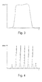
- FIG. 3 shows an example of a desired reflection spectrum for the C-band
- FIG. 4 shows a desired reflection spectrum for a number of determined frequencies
- FIG. 5 shows an example of a reflection spectrum
- FIG. 6 shows an example of the imaginary part of a target function
- FIG. 7 shows an example of a reflection spectrum after three iterative calculations
- FIG. 8 shows an example of the target function after three iterative calculations
- FIG. 9 shows an example of a reflection spectrum after 20 iterative calculations
- FIG. 10 shows an example of the target function after 20 iterative calculations.
- the present method of calculating a grating is to calculate a general grating by optimising the number of grating rulings and the position of each ruling individually in order to optimise the target function. This is the same as the process of optimising the vector z k in FIG. 1 .
- a reflection spectrum is first calculated and then the target function is formed with which the said reflection spectrum is compared with a desired reflection spectrum.
- the target function gives a high value for a reflection spectrum that lies close to the desired spectrum and a low value for a reflection spectrum that lies far from the desired spectrum.
- the target function is then optimised with respect to the positions of the rulings of the grating using standard mathematical methods.
- step a) comprises the determination of a number of wavelengths that are to be reflected or an interval of wavelengths that is to be reflected.
- a preliminary grating which has a reflection spectrum r 0 (f) that fulfils at least partially the reflections specified in step a) is calculated in step b) using a suitable known calculation method.
- the reflection spectrum r 0 (f) is compared in step c) with the characteristics that the modulated grating is to have.
- step c) On the condition that step c) has revealed differences, the reflection spectrum r 0 (f) is caused to be changed in step d) by ⁇ r(f).
- a target function G(z) is calculated in step e) not only for the position z k of each ruling of the grating, but also for each position at which sufficient space is available to create a grating ruling.
- the target function G(z) is an integral between the influence of the reflection spectrum ⁇ r(f, z) for one grating ruling and the change ⁇ r(f).
- the grating (z k ) is caused to be changed in step f), depending on the values of the target function G(z) with respect to its real part and its imaginary part, by carrying out one or several of the modifications: to add one or several rulings where space is available, to remove one or several rulings, and/or to move one or several rulings,
- step a) the steps c) to f) are repeated until the target function specifies that the grating reflects the wavelengths as specified in step a).
- a grating ruling is caused to be added in the case in which the real part Re[G(z)] of the target function is positive.
- a grating ruling is caused to be removed in the case in which the real part Re[G(z)] of the target function is negative.
- the imaginary part of the target function is caused to control a change of the positions (z k ) of the grating rulings.
- a position z that gives a value of the target function whose real part is greater than zero improves the grating.
- the effect of changing the position of a ruling from z to z+dz can be regarded as that of removing a ruling at the position z and adding a ruling at the position the z+dz.
- a new target function can be derived:
- the target function for a change of the position has a positive real part when the target function for the addition of a ruling has a negative imaginary part.
- the imaginary part of G(z) can be used to determine whether it is advantageous to move a ruling or not.
- the matrix method can be used instead in order to calculate this contribution. (Reference: Coldren, “Diode Lasers and Photonic Integrated Circuits”).
- the matrix method is used to represent a grating with a series of matrices corresponding to the rulings of the grating and the delay between the rulings.
- a delay function (a uniform part of the waveguide without any etched rulings) is represented by the matrix:
- T delay ⁇ ( L ) ( exp ⁇ ( i ⁇ ⁇ ⁇ L ) 0 0 exp ⁇ ( - i ⁇ ⁇ ⁇ L ) )
- beta may be complex in the case in which losses arise.
- the reflection of a grating ruling can be represented through:
- T groove 1 t one ⁇ ( ⁇ ) ⁇ ( 1 - r one ⁇ ( ⁇ ) r one ⁇ ( ⁇ ) 1 )
- T grating ⁇ k ⁇ T delay ⁇ ( z k - z k - 1 ) ⁇ T groove
- the product is calculated across all rulings k of the grating.
- the contribution from an individual grating ruling at z k can in this way be calculated by repeating the calculation for T grating and r grating while omitting z k during the second calculation and subsequently calculating the difference.
- ⁇ r k (beta) r grating ⁇ r grating — without — groove — at — zk
- ⁇ r k (f, z) r grating (f) ⁇ r grating2 (f)
- r grating (f) is the reflection spectrum for the complete grating
- r grating2 (f) is the reflection spectrum for the grating from which the ruling at z has been omitted.
- This value can be calculated in the step e) in the algorithm for calculating the target function.
- the calculations of the reflection spectrum take place iteratively.
- the value of the reflection spectrum after three iterations is shown in FIG. 7 and the value of G shift (z) after three iterations is shown in FIG. 8 .
- the situation after 20 iterations is shown in FIGS. 9 and 10 .
Landscapes
- Physics & Mathematics (AREA)
- General Physics & Mathematics (AREA)
- Optics & Photonics (AREA)
- Engineering & Computer Science (AREA)
- Manufacturing & Machinery (AREA)
- Diffracting Gratings Or Hologram Optical Elements (AREA)
- Lasers (AREA)
- Spectrometry And Color Measurement (AREA)
Applications Claiming Priority (4)
| Application Number | Priority Date | Filing Date | Title |
|---|---|---|---|
| SE0501823A SE531353C2 (sv) | 2005-08-17 | 2005-08-17 | Metod för att framställa ett modulerat gitter för ett optimalt reflektionsspektra |
| SE0501823 | 2005-08-17 | ||
| SE0501823-9 | 2005-08-17 | ||
| PCT/SE2006/050283 WO2007021241A1 (en) | 2005-08-17 | 2006-08-16 | Method for producing a modulated grating for an optimal reflection spectrum |
Publications (2)
| Publication Number | Publication Date |
|---|---|
| US20090170229A1 US20090170229A1 (en) | 2009-07-02 |
| US7910384B2 true US7910384B2 (en) | 2011-03-22 |
Family
ID=37757828
Family Applications (1)
| Application Number | Title | Priority Date | Filing Date |
|---|---|---|---|
| US12/064,092 Active 2027-04-17 US7910384B2 (en) | 2005-08-17 | 2006-08-16 | Method for producing a modulated grating for an optimal reflection spectrum |
Country Status (5)
| Country | Link |
|---|---|
| US (1) | US7910384B2 (de) |
| EP (1) | EP1946158B1 (de) |
| AT (1) | ATE537472T1 (de) |
| SE (1) | SE531353C2 (de) |
| WO (1) | WO2007021241A1 (de) |
Citations (6)
| Publication number | Priority date | Publication date | Assignee | Title |
|---|---|---|---|---|
| EP0847116A2 (de) | 1992-03-06 | 1998-06-10 | Nippon Telegraph And Telephone Corporation | Verteiler Reflektor und Halbleiterlaser mit abstimmbarer Wellenlänge |
| WO2000054080A2 (en) | 1999-03-05 | 2000-09-14 | Fujitsu Telecommunications Europe Ltd. | Aperiodic longitudinal gratings and optimisation method |
| WO2003010586A2 (en) | 2001-07-25 | 2003-02-06 | Teraxion Inc. | Optical structure for the compensation of chromatic dispersion |
| US20040001671A1 (en) | 2002-07-01 | 2004-01-01 | Ansheng Liu | Waveguide-based bragg gratings with spectral sidelobe suppression and method thereof |
| US20050018964A1 (en) | 2003-07-24 | 2005-01-27 | Yu Chen | Compensation of Bragg wavelength shift in a grating assisted direct coupler |
| US7083995B2 (en) * | 1999-11-26 | 2006-08-01 | Nec Electronics Corporation | Optical semiconductor device and process for producing the same |
Family Cites Families (2)
| Publication number | Priority date | Publication date | Assignee | Title |
|---|---|---|---|---|
| US5113286A (en) | 1990-09-27 | 1992-05-12 | At&T Bell Laboratories | Diffraction grating apparatus and method of forming a surface relief pattern in diffraction grating apparatus |
| US6993222B2 (en) * | 1999-03-03 | 2006-01-31 | Rj Mears, Llc | Optical filter device with aperiodically arranged grating elements |
-
2005
- 2005-08-17 SE SE0501823A patent/SE531353C2/sv not_active IP Right Cessation
-
2006
- 2006-08-16 WO PCT/SE2006/050283 patent/WO2007021241A1/en not_active Ceased
- 2006-08-16 EP EP06784209A patent/EP1946158B1/de not_active Not-in-force
- 2006-08-16 AT AT06784209T patent/ATE537472T1/de active
- 2006-08-16 US US12/064,092 patent/US7910384B2/en active Active
Patent Citations (6)
| Publication number | Priority date | Publication date | Assignee | Title |
|---|---|---|---|---|
| EP0847116A2 (de) | 1992-03-06 | 1998-06-10 | Nippon Telegraph And Telephone Corporation | Verteiler Reflektor und Halbleiterlaser mit abstimmbarer Wellenlänge |
| WO2000054080A2 (en) | 1999-03-05 | 2000-09-14 | Fujitsu Telecommunications Europe Ltd. | Aperiodic longitudinal gratings and optimisation method |
| US7083995B2 (en) * | 1999-11-26 | 2006-08-01 | Nec Electronics Corporation | Optical semiconductor device and process for producing the same |
| WO2003010586A2 (en) | 2001-07-25 | 2003-02-06 | Teraxion Inc. | Optical structure for the compensation of chromatic dispersion |
| US20040001671A1 (en) | 2002-07-01 | 2004-01-01 | Ansheng Liu | Waveguide-based bragg gratings with spectral sidelobe suppression and method thereof |
| US20050018964A1 (en) | 2003-07-24 | 2005-01-27 | Yu Chen | Compensation of Bragg wavelength shift in a grating assisted direct coupler |
Also Published As
| Publication number | Publication date |
|---|---|
| WO2007021241A1 (en) | 2007-02-22 |
| SE0501823L (sv) | 2007-02-18 |
| ATE537472T1 (de) | 2011-12-15 |
| SE531353C2 (sv) | 2009-03-03 |
| EP1946158A1 (de) | 2008-07-23 |
| EP1946158B1 (de) | 2011-12-14 |
| US20090170229A1 (en) | 2009-07-02 |
| EP1946158A4 (de) | 2010-11-24 |
Similar Documents
| Publication | Publication Date | Title |
|---|---|---|
| JP4989834B2 (ja) | サンプル格子分布型ブラッグ反射レーザー用のミラー及び空洞設計の改良 | |
| US4935930A (en) | Laser light source for generating beam collimated in at least one direction | |
| US9853418B2 (en) | Tunable laser and tuning method using the same | |
| JP2007048988A (ja) | 半導体レーザ、レーザモジュール、光学部品、レーザ装置、半導体レーザの製造方法および半導体レーザの制御方法 | |
| US6937638B2 (en) | Manufacturable sampled grating mirrors | |
| US7106778B2 (en) | Tuneable laser | |
| US6816518B2 (en) | Wavelength tunable high repetition rate optical pulse generator | |
| US12348003B2 (en) | Tunable semiconductor laser device | |
| US12174370B2 (en) | Synthesized aperiodic gratings and method of manufacture | |
| US7382817B2 (en) | V-coupled-cavity semiconductor laser | |
| US7910384B2 (en) | Method for producing a modulated grating for an optimal reflection spectrum | |
| JP4690521B2 (ja) | 広い範囲の波長で同調可能な集積化された半導体装置及び広い範囲の波長で同調可能な半導体装置のための方法 | |
| EP1058358B1 (de) | Wellenlängenabstimmbare integrierte Halbleiterlaser-Vorrichtung | |
| US7830927B2 (en) | Bragg grating reflection strength control | |
| US20070133649A1 (en) | Wavelength tunable light source | |
| CN118841829B (zh) | 一种可调谐半导体激光器阵列 | |
| US6798818B2 (en) | Method of producing distributing reflectors, and reflectors provided by the method | |
| JP2004273644A (ja) | 半導体レーザ | |
| CN119362147A (zh) | 一种基于倾斜光栅的半导体激光器装置及其制作方法 | |
| TW202534362A (zh) | 多波長雷射器的腔體結構 | |
| GB2433160A (en) | Bragg reflector grating |
Legal Events
| Date | Code | Title | Description |
|---|---|---|---|
| AS | Assignment |
Owner name: SYNTUNE AB, SWEDEN Free format text: ASSIGNMENT OF ASSIGNORS INTEREST;ASSIGNOR:WESSTROM, JAN-OLOF;REEL/FRAME:021562/0930 Effective date: 20080904 |
|
| STCF | Information on status: patent grant |
Free format text: PATENTED CASE |
|
| FEPP | Fee payment procedure |
Free format text: PAT HOLDER NO LONGER CLAIMS SMALL ENTITY STATUS, ENTITY STATUS SET TO UNDISCOUNTED (ORIGINAL EVENT CODE: STOL); ENTITY STATUS OF PATENT OWNER: LARGE ENTITY |
|
| FPAY | Fee payment |
Year of fee payment: 4 |
|
| MAFP | Maintenance fee payment |
Free format text: PAYMENT OF MAINTENANCE FEE, 8TH YEAR, LARGE ENTITY (ORIGINAL EVENT CODE: M1552); ENTITY STATUS OF PATENT OWNER: LARGE ENTITY Year of fee payment: 8 |
|
| AS | Assignment |
Owner name: II-VI DELAWARE, INC., DELAWARE Free format text: ASSIGNMENT OF ASSIGNORS INTEREST;ASSIGNOR:FINISAR CORPORATION;REEL/FRAME:052286/0001 Effective date: 20190924 |
|
| AS | Assignment |
Owner name: FINISAR CORPORATION, CALIFORNIA Free format text: ASSIGNMENT OF ASSIGNORS INTEREST;ASSIGNOR:SYNTUNE AB;REEL/FRAME:060156/0299 Effective date: 20220421 |
|
| AS | Assignment |
Owner name: JPMORGAN CHASE BANK, N.A., AS COLLATERAL AGENT, NEW YORK Free format text: SECURITY INTEREST;ASSIGNORS:II-VI INCORPORATED;II-VI DELAWARE, INC.;M CUBED TECHNOLOGIES, INC.;AND OTHERS;REEL/FRAME:060562/0254 Effective date: 20220701 |
|
| MAFP | Maintenance fee payment |
Free format text: PAYMENT OF MAINTENANCE FEE, 12TH YEAR, LARGE ENTITY (ORIGINAL EVENT CODE: M1553); ENTITY STATUS OF PATENT OWNER: LARGE ENTITY Year of fee payment: 12 |