US7894010B2 - Liquid crystal display panel and method for fabricating the same - Google Patents
Liquid crystal display panel and method for fabricating the same Download PDFInfo
- Publication number
- US7894010B2 US7894010B2 US12/289,529 US28952908A US7894010B2 US 7894010 B2 US7894010 B2 US 7894010B2 US 28952908 A US28952908 A US 28952908A US 7894010 B2 US7894010 B2 US 7894010B2
- Authority
- US
- United States
- Prior art keywords
- electrode
- data line
- thin film
- film transistor
- substrate
- Prior art date
- Legal status (The legal status is an assumption and is not a legal conclusion. Google has not performed a legal analysis and makes no representation as to the accuracy of the status listed.)
- Active, expires
Links
Images


Classifications
-
- G—PHYSICS
- G02—OPTICS
- G02F—OPTICAL DEVICES OR ARRANGEMENTS FOR THE CONTROL OF LIGHT BY MODIFICATION OF THE OPTICAL PROPERTIES OF THE MEDIA OF THE ELEMENTS INVOLVED THEREIN; NON-LINEAR OPTICS; FREQUENCY-CHANGING OF LIGHT; OPTICAL LOGIC ELEMENTS; OPTICAL ANALOGUE/DIGITAL CONVERTERS
- G02F1/00—Devices or arrangements for the control of the intensity, colour, phase, polarisation or direction of light arriving from an independent light source, e.g. switching, gating or modulating; Non-linear optics
- G02F1/01—Devices or arrangements for the control of the intensity, colour, phase, polarisation or direction of light arriving from an independent light source, e.g. switching, gating or modulating; Non-linear optics for the control of the intensity, phase, polarisation or colour
- G02F1/13—Devices or arrangements for the control of the intensity, colour, phase, polarisation or direction of light arriving from an independent light source, e.g. switching, gating or modulating; Non-linear optics for the control of the intensity, phase, polarisation or colour based on liquid crystals, e.g. single liquid crystal display cells
- G02F1/133—Constructional arrangements; Operation of liquid crystal cells; Circuit arrangements
- G02F1/1333—Constructional arrangements; Manufacturing methods
- G02F1/1343—Electrodes
- G02F1/134309—Electrodes characterised by their geometrical arrangement
-
- G—PHYSICS
- G02—OPTICS
- G02F—OPTICAL DEVICES OR ARRANGEMENTS FOR THE CONTROL OF LIGHT BY MODIFICATION OF THE OPTICAL PROPERTIES OF THE MEDIA OF THE ELEMENTS INVOLVED THEREIN; NON-LINEAR OPTICS; FREQUENCY-CHANGING OF LIGHT; OPTICAL LOGIC ELEMENTS; OPTICAL ANALOGUE/DIGITAL CONVERTERS
- G02F1/00—Devices or arrangements for the control of the intensity, colour, phase, polarisation or direction of light arriving from an independent light source, e.g. switching, gating or modulating; Non-linear optics
- G02F1/01—Devices or arrangements for the control of the intensity, colour, phase, polarisation or direction of light arriving from an independent light source, e.g. switching, gating or modulating; Non-linear optics for the control of the intensity, phase, polarisation or colour
- G02F1/13—Devices or arrangements for the control of the intensity, colour, phase, polarisation or direction of light arriving from an independent light source, e.g. switching, gating or modulating; Non-linear optics for the control of the intensity, phase, polarisation or colour based on liquid crystals, e.g. single liquid crystal display cells
- G02F1/133—Constructional arrangements; Operation of liquid crystal cells; Circuit arrangements
- G02F1/1333—Constructional arrangements; Manufacturing methods
- G02F1/1343—Electrodes
-
- G—PHYSICS
- G02—OPTICS
- G02F—OPTICAL DEVICES OR ARRANGEMENTS FOR THE CONTROL OF LIGHT BY MODIFICATION OF THE OPTICAL PROPERTIES OF THE MEDIA OF THE ELEMENTS INVOLVED THEREIN; NON-LINEAR OPTICS; FREQUENCY-CHANGING OF LIGHT; OPTICAL LOGIC ELEMENTS; OPTICAL ANALOGUE/DIGITAL CONVERTERS
- G02F1/00—Devices or arrangements for the control of the intensity, colour, phase, polarisation or direction of light arriving from an independent light source, e.g. switching, gating or modulating; Non-linear optics
- G02F1/01—Devices or arrangements for the control of the intensity, colour, phase, polarisation or direction of light arriving from an independent light source, e.g. switching, gating or modulating; Non-linear optics for the control of the intensity, phase, polarisation or colour
- G02F1/13—Devices or arrangements for the control of the intensity, colour, phase, polarisation or direction of light arriving from an independent light source, e.g. switching, gating or modulating; Non-linear optics for the control of the intensity, phase, polarisation or colour based on liquid crystals, e.g. single liquid crystal display cells
- G02F1/133—Constructional arrangements; Operation of liquid crystal cells; Circuit arrangements
- G02F1/1333—Constructional arrangements; Manufacturing methods
- G02F1/1335—Structural association of cells with optical devices, e.g. polarisers or reflectors
- G02F1/133509—Filters, e.g. light shielding masks
- G02F1/133512—Light shielding layers, e.g. black matrix
-
- G—PHYSICS
- G02—OPTICS
- G02F—OPTICAL DEVICES OR ARRANGEMENTS FOR THE CONTROL OF LIGHT BY MODIFICATION OF THE OPTICAL PROPERTIES OF THE MEDIA OF THE ELEMENTS INVOLVED THEREIN; NON-LINEAR OPTICS; FREQUENCY-CHANGING OF LIGHT; OPTICAL LOGIC ELEMENTS; OPTICAL ANALOGUE/DIGITAL CONVERTERS
- G02F1/00—Devices or arrangements for the control of the intensity, colour, phase, polarisation or direction of light arriving from an independent light source, e.g. switching, gating or modulating; Non-linear optics
- G02F1/01—Devices or arrangements for the control of the intensity, colour, phase, polarisation or direction of light arriving from an independent light source, e.g. switching, gating or modulating; Non-linear optics for the control of the intensity, phase, polarisation or colour
- G02F1/13—Devices or arrangements for the control of the intensity, colour, phase, polarisation or direction of light arriving from an independent light source, e.g. switching, gating or modulating; Non-linear optics for the control of the intensity, phase, polarisation or colour based on liquid crystals, e.g. single liquid crystal display cells
- G02F1/133—Constructional arrangements; Operation of liquid crystal cells; Circuit arrangements
- G02F1/1333—Constructional arrangements; Manufacturing methods
- G02F1/1343—Electrodes
- G02F1/134309—Electrodes characterised by their geometrical arrangement
- G02F1/134318—Electrodes characterised by their geometrical arrangement having a patterned common electrode
-
- G—PHYSICS
- G02—OPTICS
- G02F—OPTICAL DEVICES OR ARRANGEMENTS FOR THE CONTROL OF LIGHT BY MODIFICATION OF THE OPTICAL PROPERTIES OF THE MEDIA OF THE ELEMENTS INVOLVED THEREIN; NON-LINEAR OPTICS; FREQUENCY-CHANGING OF LIGHT; OPTICAL LOGIC ELEMENTS; OPTICAL ANALOGUE/DIGITAL CONVERTERS
- G02F1/00—Devices or arrangements for the control of the intensity, colour, phase, polarisation or direction of light arriving from an independent light source, e.g. switching, gating or modulating; Non-linear optics
- G02F1/01—Devices or arrangements for the control of the intensity, colour, phase, polarisation or direction of light arriving from an independent light source, e.g. switching, gating or modulating; Non-linear optics for the control of the intensity, phase, polarisation or colour
- G02F1/13—Devices or arrangements for the control of the intensity, colour, phase, polarisation or direction of light arriving from an independent light source, e.g. switching, gating or modulating; Non-linear optics for the control of the intensity, phase, polarisation or colour based on liquid crystals, e.g. single liquid crystal display cells
- G02F1/133—Constructional arrangements; Operation of liquid crystal cells; Circuit arrangements
- G02F1/136—Liquid crystal cells structurally associated with a semi-conducting layer or substrate, e.g. cells forming part of an integrated circuit
- G02F1/13606—Liquid crystal cells structurally associated with a semi-conducting layer or substrate, e.g. cells forming part of an integrated circuit having means for reducing parasitic capacitance
-
- G—PHYSICS
- G02—OPTICS
- G02F—OPTICAL DEVICES OR ARRANGEMENTS FOR THE CONTROL OF LIGHT BY MODIFICATION OF THE OPTICAL PROPERTIES OF THE MEDIA OF THE ELEMENTS INVOLVED THEREIN; NON-LINEAR OPTICS; FREQUENCY-CHANGING OF LIGHT; OPTICAL LOGIC ELEMENTS; OPTICAL ANALOGUE/DIGITAL CONVERTERS
- G02F2201/00—Constructional arrangements not provided for in groups G02F1/00 - G02F7/00
- G02F2201/12—Constructional arrangements not provided for in groups G02F1/00 - G02F7/00 electrode
- G02F2201/124—Constructional arrangements not provided for in groups G02F1/00 - G02F7/00 electrode interdigital
-
- G—PHYSICS
- G02—OPTICS
- G02F—OPTICAL DEVICES OR ARRANGEMENTS FOR THE CONTROL OF LIGHT BY MODIFICATION OF THE OPTICAL PROPERTIES OF THE MEDIA OF THE ELEMENTS INVOLVED THEREIN; NON-LINEAR OPTICS; FREQUENCY-CHANGING OF LIGHT; OPTICAL LOGIC ELEMENTS; OPTICAL ANALOGUE/DIGITAL CONVERTERS
- G02F2201/00—Constructional arrangements not provided for in groups G02F1/00 - G02F7/00
- G02F2201/40—Arrangements for improving the aperture ratio
-
- G—PHYSICS
- G02—OPTICS
- G02F—OPTICAL DEVICES OR ARRANGEMENTS FOR THE CONTROL OF LIGHT BY MODIFICATION OF THE OPTICAL PROPERTIES OF THE MEDIA OF THE ELEMENTS INVOLVED THEREIN; NON-LINEAR OPTICS; FREQUENCY-CHANGING OF LIGHT; OPTICAL LOGIC ELEMENTS; OPTICAL ANALOGUE/DIGITAL CONVERTERS
- G02F2201/00—Constructional arrangements not provided for in groups G02F1/00 - G02F7/00
- G02F2201/50—Protective arrangements
Definitions
- the present invention relates to a liquid crystal display panel and a method for fabricating the same. More particularly, the present invention relates to a liquid crystal display panel and a method for fabricating the same which can improve aperture and prevent a brightness deviation between lots.
- a liquid crystal display device displays a picture by controlling a light transmittivity of liquid crystals having dielectric anisotropy with an electric field.
- the liquid crystal display device controls the light transmittivity of liquid crystals with the electric field for displaying the picture.
- an in-plane switching type liquid crystal display device drives the liquid crystals in an in-plane switch mode with a horizontal electric field formed between pixel electrodes and a common electrode arranged in parallel on a lower substrate.
- the in-plane switching type liquid crystal display device includes a thin film transistor substrate and a color filter substrate which are bonded to face each other, spacers for maintaining a cell gap between the two substrates, and liquid crystals filled in the cell gap.
- the color filter substrate includes a color filter 34 for displaying colors, a black matrix 32 for preventing light from leaking, and an alignment film coated thereon for alignment of the liquid crystals.
- a pixel electrode (not shown) and a common electrode 22 arranged in parallel, a shielding electrode 24 for shielding a data signal to a data line 14 , a thin film transistor connected to the common electrode 22 and the pixel electrode, and an alignment film coated thereon for alignment of liquid crystals.
- the in-plane switching type liquid crystal display device has a width of a black matrix 32 formed greater by C taking a light leakage from between the common electrode 22 and the data line 14 , i.e., A region, and a bonding process margin (B region) into account. As the width of the black matrix 32 becomes greater, improvement of an aperture of the liquid crystal display panel becomes a problem.
- the present invention is directed to a liquid crystal display panel and a method for fabricating the same.
- An advantage of the present invention is to provide a liquid crystal display panel and a method for fabricating the same which can improve aperture and prevent a brightness deviation between lots.
- a liquid crystal display panel includes a thin film transistor formed on a lower substrate so as to be connected to a gate line and a data line, a pixel electrode connected to a drain electrode of the thin film transistor, a common electrode for forming a horizontal electric field with the pixel electrode, a connection electrode overlapped with, and connected to the data line, and a black matrix on an upper substrate opposite to the lower substrate for forming a vertical electric field with the connection electrode.
- a method for fabricating a liquid crystal display panel includes the steps of providing a thin film transistor substrate including a thin film transistor formed on a lower substrate so as to be connected to a gate line and a data line, a pixel electrode connected to a drain electrode of the thin film transistor, a common electrode for forming a horizontal electric field with the pixel electrode, and a connection electrode overlapped with, and connected to the data line, providing a color filter substrate including a black matrix on an upper substrate opposite to the lower substrate for forming a vertical electric field with the connection electrode, and bonding the thin film transistor substrate and the color filter substrate together.
- FIG. 1 is a sectional view illustrating a related art liquid crystal display panel.
- FIG. 2 is a plan view illustrating a liquid crystal display panel in accordance with an embodiment of the present invention.
- FIG. 3 is a sectional view illustrating the liquid crystal display panel across a line I-I′ in FIG. 2 .
- FIG. 4 is a plan view illustrating a color filter substrate of a liquid crystal display panel in accordance with an embodiment of the present invention.
- FIGS. 5A and 5B are a plan view and a sectional view for describing a method for fabricating the gate metal pattern shown in FIGS. 2 and 3 , respectively.
- FIGS. 6A and 6B are a plan view and a sectional view for describing a method for fabricating the semiconductor pattern and the data metal pattern shown in FIGS. 2 and 3 , respectively.
- FIGS. 7A and 7B are a plan view and a sectional view for describing a method for fabricating the protective film shown in FIGS. 2 and 3 , respectively.
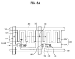
- FIGS. 8A and 8B are a plan view and a sectional view for describing a method for fabricating a pixel electrode and a connection electrode, respectively.
- FIGS. 9A and 9B are sectional views of a liquid crystal display panel in accordance with a preferred embodiment of the present invention.
- FIG. 2 is a plan view illustrating a liquid crystal display panel in accordance with an embodiment of the present invention
- FIG. 3 is a sectional view illustrating the liquid crystal display panel across a line I-I′ in FIG. 2 .
- the liquid crystal display panel includes a color filter substrate and a thin film transistor substrate bonded together with liquid crystals disposed therebetween.
- the color filter substrate includes a color filter 204 and a black matrix 202 .
- the color filter 204 includes red R, green G, and blue B color filters 204 for reproducing colors.
- the red R, green G, and blue B color filters 204 absorb or transmit lights of specific wave lengths by means of red, green, blue pigments the red R, green G, and blue B color filter 204 contain for displaying the red, green, and blue colors, respectively.
- the black matrix 202 marks pixel regions on which the color filters 204 are to be formed and is formed to overlap with a gate line 102 , a data line 104 , and a thin film transistor 130 on the thin film transistor substrate.
- the black matrix 202 shields light transmission caused by unwanted liquid crystal alignment for improving a contrast of the liquid crystal display device, and shields direct light direction to the thin film transistor 130 for preventing a light leakage current from the thin film transistor 130 .
- the black matrix 202 is constructed of a metal layer of copper Cu, aluminum Al, chromium Cr, an aluminum alloy, or so on, and has a ground voltage GND applied thereto to form a vertical electric filed with a connection electrode 152 .
- the black matrix 202 may be formed among the red, green, blue color filters 204 , or as shown in FIG. 4 , on the color filers 204 .
- an overcoat layer may be formed, additionally.
- the thin film transistor substrate has a thin film transistor 130 , a pixel electrode 122 , a common electrode 124 , and a connection electrode 152 .
- the thin film transistor 130 charges a pixel signal supplied from the data line in response to a scan signal supplied to the gate line to the pixel electrode 122 and maintains the pixel signal charged at the pixel electrode 122 .
- the thin film transistor 130 has a gate electrode 106 , a source electrode 108 , a drain electrode 110 , an active layer 114 , and an ohmic contact layer 116 .
- the gate electrode 106 is connected to the gate line 102 for having the scan signal supplied thereto from the gate line 102 .
- the source electrode 108 is connected to the data line 104 for having the pixel signal supplied thereto from the data line 104 .
- the drain electrode 110 formed opposite to the source electrode 108 with a channel portion of the active layer 114 disposed therebetween for supplying the pixel signal from the data line 104 to the pixel electrode 122 .
- the active layer overlapped with the gate electrode 106 with a gate insulating film 112 disposed therebetween to form the channel portion between the source and the drain electrodes 108 , and 110 .
- the ohmic contact layer 116 is formed between the source electrode 108 and the drain electrode 110 and the active layer 114 , i.e., on the active layer 114 excluding the channel portion.
- the ohmic contact layer 116 serves to reduce electric contact resistance between the source and drain electrodes 108 and 110 and the active layer 114 .
- a semiconductor pattern including the active layer 114 and the ohmic contact layer 116 is overlapped, not only with the source and drain electrodes 108 and 110 , but also with a data metal pattern including the data line 104 in view of fabrication process.
- the pixel electrode 122 is connected to the drain electrode 110 of the thin film transistor 130 through a pixel contact hole 120 . According to this, the pixel electrode 122 has the pixel signal supplied thereto from the data line 140 through the thin film transistor 130 .
- the pixel electrode 122 has a first electrode portion 122 a parallel to the gate line 102 , and a second electrode portion 122 b extended from the first electrode portion 122 a perpendicular thereto.
- the common electrode 124 is connected to the common line 126 for having a common voltage supplied thereto through the common line 126 .
- the common electrode 122 is formed of the same material with the pixel electrode 122 on the same plane, or the same material with or a material different from the pixel electrode 122 on a plane different from the pixel electrode 122 .
- the common electrode 124 is formed on the substrate 101 as a gate metal layer
- the pixel electrode 122 is formed on the protective film 118 as a transparent conductive layer, such that the common electrode 124 and the pixel electrode 122 are formed on planes and of materials different from each other.
- the common electrode 124 is formed parallel to the second electrode portion 122 b of the pixel electrode 122 . According to this, a horizontal electric field is formed between the pixel electrode 122 having the pixel voltage signal supplied thereto and the common electrode 124 having the common voltage supplied thereto.
- the horizontal electric field rotates the liquid crystal molecules aligned in a horizontal direction between the thin film transistor substrate and the color filter substrate owing to dielectric anisotropy.
- the transmittivity of light through the sub-pixel region varies with extents of rotation of the liquid crystal molecules, to produce a picture.
- connection electrode 152 is connected to the data line 104 through a second contact hole 150 in the protective film 118 .
- the connection electrode 152 overlaps with the common electrode 124 partially with the gate insulating film 112 and the protective film 118 disposed therebetween. According to this, the connection electrode 152 prevents a light from leaking through a gap between the data line 104 and the common electrode 124 .
- a total resistance of the data line 104 is reduced, and pixel signals are supplied to the data line 104 as well as to the connection electrode 152 in contact with the data line 104 too, making the data line 104 and the connection electrode 152 to be on the same level.
- the partial overlap of the connection electrode 152 and the common electrode 124 eliminates the necessity for forming the width of the black matrix 202 greater.
- the aperture of the liquid crystal display panel can be improved.
- the prevention of light leakage and the securing of the bonding process margin permit to prevent a brightness deviation between lots from taking place.
- connection electrode 152 By applying the ground voltage GND to the black matrix 202 opposite to the connection electrode 152 , a vertical electric field is formed between the connection electrode 152 and the black matrix 202 . According to this, crosstalk caused by parasitic capacitor between the data line 104 and the pixel electrode 122 can be prevented.
- the static electricity is dispersed owing to an electric field between the connection electrode 152 and the black matrix 202 having a plurality of gate lines 102 and data lines 104 formed thereon. According to this, by removing ITO (Indium Tin Oxide) formed on the color filter substrate for prevention of the static electricity, the transmittivity can be improved.
- ITO Indium Tin Oxide
- the transmittivity is reduced due to the ITO (Indium Tin Oxide) formed for prevention of the static electricity that blocks an external light, the transmittivity can be improved by removing the ITO.
- ITO Indium Tin Oxide
- FIGS. 5A and 5B are a plan view and a sectional view for describing a method for fabricating the gate metal pattern shown in FIGS. 2 and 3 , respectively.
- a gate metal pattern including a gate line 102 , a gate electrode 106 , a common line 126 , and a common electrode 124 is formed on a lower substrate 101 .
- a gate metal layer is deposited on the lower substrate 101 by sputtering or the like.
- the gate metal layer may be constructed of a single layer of metal, such as Mo, Ti, Cu, AlNd, Al, Cr, Mo alloys, Cu alloys, Al alloys, or a stack of two or more than two layers of above metals. Then, by photolithography and etching, the gate metal layer is patterned, to form the gate metal pattern including the gate line 102 , the gate electrode 106 , the common line 126 , and the common electrode 124 .
- FIGS. 6A and 6B are a plan view and a sectional view for describing a method for fabricating the semiconductor pattern and the data metal pattern shown in FIGS. 2 and 3 , respectively.
- a gate insulating film 112 is formed on the lower substrate 101 having the gate metal pattern formed thereon, and a data metal pattern including a data line 104 , a source electrode 108 , and a drain electrode 110 and a semiconductor pattern including an active layer 114 and an ohmic contact layer 116 overlapped under and along the data metal pattern are formed on the gate insulating film 112 .
- the semiconductor pattern and the data metal pattern are formed by one mask process using a slit mask or a half tone.
- the gate insulating film 112 an amorphous silicon layer, an amorphous silicon layer doped with impurities n + or p + , and a data metal layer are formed in succession. Then, after coating photoresist on the data metal layer, the photoresist is subject to exposure and development by photolithography using a slit mask, to form a photoresist pattern having a step.
- the data metal layer is patterned, to form the data metal pattern, and the underlying semiconductor pattern.
- the photoresist pattern is ashed by using an ashing process using oxygen O 2 plasma.
- the data metal pattern exposed thus and the underlying ohmic contact layer are removed, to separate the source electrode 108 and the drain electrode 110 , and expose the active layer 114 .
- the photoresist pattern remained on the data metal pattern is removed by stripping.
- FIGS. 7A and 7B are a plan view and a sectional view for describing a method for fabricating the protective film shown in FIGS. 2 and 3 , respectively.
- a protective film 118 is formed on the gate insulating film 112 having the data metal pattern formed thereon.
- the protective film 118 is formed of an inorganic insulating material the same with the gate insulating film 112 or an organic insulating film such as acryl resin.
- a first contact hole 120 and a second contact hole 150 passed through the protective film 118 are formed.
- the first contact hole 120 is passed through the protective film 118 to expose the drain electrode 110
- the second contact hole 150 is passed through the protective film to expose the data line 104 .
- FIGS. 8A and 8B are a plan view and a sectional view for describing a method for fabricating a pixel electrode and a connection electrode, respectively.
- a conductive film pattern including a pixel electrode 122 connected to the drain electrode 110 , and a connection electrode 152 connected to the data line 104 is formed.
- a transparent, or non-transparent conductive layer is formed on the protective film 118 by deposition, such as sputtering.
- the transparent conductive layer is formed of tin oxide TI, indium tin oxide ITO, indium zinc oxide IZO, indium tin zinc oxide ITZO, or so on.
- the non-transparent conductive layer is formed of Cr, Mo, Cu, Al, a molybdenum alloy, a molybdenum titan alloy, an aluminum alloy, or so on.
- the liquid crystal display panel is formed as shown in FIGS. 9A and 9B by bonding the thin film transistor substrate, and the color filter substrate having red R, green G, and blue B color filters 204 formed on a lower substrate for reproducing red R, green G, and blue B colors and a black matrix 202 formed on or under the color filters 204 both formed as shown in FIGS. 5A to 8B together.
- the liquid crystal display panel and the method for fabricating the same have the following advantages.
- connection electrode connected to the data line and partially overlapped with the common electrode adjacent to the data line with the protective film and the gate insulating film therebetween permits to prevent a light from leaking through a gap between the data line and the common electrode.
- the prevention of the leakage of light with the connection electrode permits to reduce a width of the black matrix, and a line width of the common electrode, which improves aperture and compensate for a brightness deviation between lots.
- a crosstalk can prevented, caused by a parasitic capacitor formed between he pixel electrode and the data line.
Landscapes
- Physics & Mathematics (AREA)
- Nonlinear Science (AREA)
- Mathematical Physics (AREA)
- Chemical & Material Sciences (AREA)
- Crystallography & Structural Chemistry (AREA)
- General Physics & Mathematics (AREA)
- Optics & Photonics (AREA)
- Geometry (AREA)
- Liquid Crystal (AREA)
Abstract
Description
Claims (8)
Applications Claiming Priority (3)
| Application Number | Priority Date | Filing Date | Title |
|---|---|---|---|
| KR1020070109620A KR101374108B1 (en) | 2007-10-30 | 2007-10-30 | Liquid crystal display panel and manufacturing method thereof |
| KR10-2007-109620 | 2007-10-30 | ||
| KR2007-109620 | 2007-10-30 |
Publications (2)
| Publication Number | Publication Date |
|---|---|
| US20090109363A1 US20090109363A1 (en) | 2009-04-30 |
| US7894010B2 true US7894010B2 (en) | 2011-02-22 |
Family
ID=40582356
Family Applications (1)
| Application Number | Title | Priority Date | Filing Date |
|---|---|---|---|
| US12/289,529 Active 2029-06-18 US7894010B2 (en) | 2007-10-30 | 2008-10-29 | Liquid crystal display panel and method for fabricating the same |
Country Status (2)
| Country | Link |
|---|---|
| US (1) | US7894010B2 (en) |
| KR (1) | KR101374108B1 (en) |
Cited By (1)
| Publication number | Priority date | Publication date | Assignee | Title |
|---|---|---|---|---|
| US9581849B2 (en) | 2013-03-22 | 2017-02-28 | Semiconductor Energy Laboratory Co., Ltd. | Liquid crystal display device |
Families Citing this family (7)
| Publication number | Priority date | Publication date | Assignee | Title |
|---|---|---|---|---|
| KR101374108B1 (en) * | 2007-10-30 | 2014-03-13 | 엘지디스플레이 주식회사 | Liquid crystal display panel and manufacturing method thereof |
| US8749738B2 (en) * | 2011-12-02 | 2014-06-10 | Shenzhen China Star Optoelectronics Technology Co., Ltd. | Liquid crystal panel and manufacturing method thereof, and liquid crystal display |
| CN102495493A (en) * | 2011-12-02 | 2012-06-13 | 深圳市华星光电技术有限公司 | Manufacturing method for liquid crystal panel, liquid crystal panel and liquid crystal display device |
| KR101283365B1 (en) * | 2011-12-08 | 2013-07-08 | 엘지디스플레이 주식회사 | Liquid crystal display device |
| CN104916648A (en) * | 2015-06-11 | 2015-09-16 | 京东方科技集团股份有限公司 | Array substrate, preparation method and display device |
| CN105607369B (en) * | 2016-01-05 | 2019-03-26 | 京东方科技集团股份有限公司 | Array substrate, liquid crystal display panel and display device |
| KR102808070B1 (en) * | 2020-12-23 | 2025-05-14 | 엘지디스플레이 주식회사 | Liquid Crystal Display Device |
Citations (4)
| Publication number | Priority date | Publication date | Assignee | Title |
|---|---|---|---|---|
| US6014190A (en) * | 1995-11-30 | 2000-01-11 | Samsung Electronics Co., Ltd. | In-plane switching liquid crystal display and a manufacturing method thereof |
| US20070159586A1 (en) * | 2005-10-19 | 2007-07-12 | Samsung Electronics Co., Ltd. | Liquid crystal display |
| US20080136990A1 (en) * | 2006-10-31 | 2008-06-12 | Semiconductor Energy Laboratory Co., Ltd. | Liquid crystal display device and electronic device |
| US20090109363A1 (en) * | 2007-10-30 | 2009-04-30 | Sang Hee Yu | Liquid crystal display panel and method for fabricating the same |
-
2007
- 2007-10-30 KR KR1020070109620A patent/KR101374108B1/en active Active
-
2008
- 2008-10-29 US US12/289,529 patent/US7894010B2/en active Active
Patent Citations (4)
| Publication number | Priority date | Publication date | Assignee | Title |
|---|---|---|---|---|
| US6014190A (en) * | 1995-11-30 | 2000-01-11 | Samsung Electronics Co., Ltd. | In-plane switching liquid crystal display and a manufacturing method thereof |
| US20070159586A1 (en) * | 2005-10-19 | 2007-07-12 | Samsung Electronics Co., Ltd. | Liquid crystal display |
| US20080136990A1 (en) * | 2006-10-31 | 2008-06-12 | Semiconductor Energy Laboratory Co., Ltd. | Liquid crystal display device and electronic device |
| US20090109363A1 (en) * | 2007-10-30 | 2009-04-30 | Sang Hee Yu | Liquid crystal display panel and method for fabricating the same |
Cited By (3)
| Publication number | Priority date | Publication date | Assignee | Title |
|---|---|---|---|---|
| US9581849B2 (en) | 2013-03-22 | 2017-02-28 | Semiconductor Energy Laboratory Co., Ltd. | Liquid crystal display device |
| US10317717B2 (en) | 2013-03-22 | 2019-06-11 | Semiconductor Energy Laboratory Co., Ltd. | Liquid crystal display device |
| US10901255B2 (en) | 2013-03-22 | 2021-01-26 | Semiconductor Energy Laboratory Co., Ltd. | Liquid crystal display device |
Also Published As
| Publication number | Publication date |
|---|---|
| KR101374108B1 (en) | 2014-03-13 |
| US20090109363A1 (en) | 2009-04-30 |
| KR20090043838A (en) | 2009-05-07 |
Similar Documents
| Publication | Publication Date | Title |
|---|---|---|
| US8111363B2 (en) | Liquid crystal display device and fabricating method thereof | |
| US7190419B2 (en) | Liquid crystal display device and method of fabricating the same | |
| US8013969B2 (en) | Liquid crystal display device comprising a protective film so that the protective film borders with one end of a transparent conductive pattern | |
| US7858984B2 (en) | Liquid crystal display device having a double layered structure and a single layered structure on the same layer | |
| US7348198B2 (en) | Liquid crystal display device and fabricating method thereof | |
| US7688414B2 (en) | Method for fabricating a liquid crystal display device and an LCD device thereby | |
| KR101126396B1 (en) | Thin film transistor array substrate and fabricating method thereof | |
| KR101980773B1 (en) | Thin film transistor substrate having color filter and method of fabricating the same | |
| US7170576B2 (en) | Thin film transistor array substrate and fabricating method thereof | |
| US20070002249A1 (en) | Liquid crystal display device and fabricating method thereof | |
| US7894010B2 (en) | Liquid crystal display panel and method for fabricating the same | |
| JP2008165230A (en) | Fringe field type liquid crystal display panel and manufacturing method thereof | |
| KR20040050311A (en) | Liquid Crystal Display Device and Method for fabricating the same | |
| US8400600B2 (en) | Liquid crystal display device and fabricating method thereof | |
| KR101980774B1 (en) | Thin film transistor substrate having color filter and method of fabricating the same | |
| US7990510B2 (en) | Liquid crystal display device | |
| US9224824B2 (en) | Display device substrate and display device equipped with same | |
| KR20080042466A (en) | LCD panel and manufacturing method | |
| KR20080054629A (en) | Thin film transistor array substrate and manufacturing method thereof | |
| US20120236225A1 (en) | Display device substrate, manufacturing method of display device substrate, display device, and manufacturing method of display device | |
| KR20060061574A (en) | Manufacturing method of liquid crystal display device | |
| KR20040084595A (en) | Liquid crystal display apparatus of horizontal electronic field applying type and fabricating method thereof |
Legal Events
| Date | Code | Title | Description |
|---|---|---|---|
| AS | Assignment |
Owner name: LG DISPLAY CO., LTD., KOREA, REPUBLIC OF Free format text: ASSIGNMENT OF ASSIGNORS INTEREST;ASSIGNORS:YU, SANG HEE;LEE, JOON DONG;LEE, DEUK SU;REEL/FRAME:021827/0798 Effective date: 20081029 |
|
| STCF | Information on status: patent grant |
Free format text: PATENTED CASE |
|
| FEPP | Fee payment procedure |
Free format text: PAYOR NUMBER ASSIGNED (ORIGINAL EVENT CODE: ASPN); ENTITY STATUS OF PATENT OWNER: LARGE ENTITY |
|
| FPAY | Fee payment |
Year of fee payment: 4 |
|
| MAFP | Maintenance fee payment |
Free format text: PAYMENT OF MAINTENANCE FEE, 8TH YEAR, LARGE ENTITY (ORIGINAL EVENT CODE: M1552) Year of fee payment: 8 |
|
| MAFP | Maintenance fee payment |
Free format text: PAYMENT OF MAINTENANCE FEE, 12TH YEAR, LARGE ENTITY (ORIGINAL EVENT CODE: M1553); ENTITY STATUS OF PATENT OWNER: LARGE ENTITY Year of fee payment: 12 |
|
| AS | Assignment |
Owner name: SAMSUNG DISPLAY CO., LTD., KOREA, REPUBLIC OF Free format text: ASSIGNMENT OF ASSIGNORS INTEREST;ASSIGNOR:LG DISPLAY CO., LTD.;REEL/FRAME:071529/0841 Effective date: 20250519 |