US7889204B2 - Processor architecture for executing wide transform slice instructions - Google Patents
Processor architecture for executing wide transform slice instructionsInfo
- Publication number
- US7889204B2 US7889204B2 US11/982,106 US98210607A US7889204B2 US 7889204 B2 US7889204 B2 US 7889204B2 US 98210607 A US98210607 A US 98210607A US 7889204 B2 US7889204 B2 US 7889204B2
- Authority
- US
- United States
- Prior art keywords
- wide
- wide operand
- operand
- storage
- register
- Prior art date
- Legal status (The legal status is an assumption and is not a legal conclusion. Google has not performed a legal analysis and makes no representation as to the accuracy of the status listed.)
- Expired - Fee Related
Links
- 230000015654 memory Effects 0.000 claims abstract description 729
- 238000000034 method Methods 0.000 claims abstract description 201
- 238000003860 storage Methods 0.000 claims description 149
- 239000011159 matrix material Substances 0.000 claims description 112
- 239000013598 vector Substances 0.000 claims description 106
- 238000007667 floating Methods 0.000 claims description 22
- 238000012545 processing Methods 0.000 claims description 22
- 238000000605 extraction Methods 0.000 claims description 18
- 238000012937 correction Methods 0.000 claims description 8
- 230000004044 response Effects 0.000 claims description 6
- 230000000977 initiatory effect Effects 0.000 claims description 4
- 230000008901 benefit Effects 0.000 abstract description 9
- 230000006870 function Effects 0.000 description 82
- 238000005192 partition Methods 0.000 description 68
- 230000000694 effects Effects 0.000 description 39
- 230000014616 translation Effects 0.000 description 39
- 238000010586 diagram Methods 0.000 description 38
- 238000013519 translation Methods 0.000 description 38
- 230000000875 corresponding effect Effects 0.000 description 31
- 230000007246 mechanism Effects 0.000 description 29
- 238000012546 transfer Methods 0.000 description 28
- 230000001419 dependent effect Effects 0.000 description 27
- 239000000872 buffer Substances 0.000 description 26
- 230000008569 process Effects 0.000 description 26
- 238000013461 design Methods 0.000 description 25
- 238000012360 testing method Methods 0.000 description 24
- 238000007792 addition Methods 0.000 description 22
- 230000011664 signaling Effects 0.000 description 22
- 230000002829 reductive effect Effects 0.000 description 18
- 230000001965 increasing effect Effects 0.000 description 16
- 230000008520 organization Effects 0.000 description 15
- 230000009977 dual effect Effects 0.000 description 14
- 238000007726 management method Methods 0.000 description 14
- 238000013507 mapping Methods 0.000 description 13
- 238000011084 recovery Methods 0.000 description 13
- 244000126822 Albuca minor Species 0.000 description 12
- 230000000670 limiting effect Effects 0.000 description 12
- 238000001693 membrane extraction with a sorbent interface Methods 0.000 description 12
- 230000001343 mnemonic effect Effects 0.000 description 12
- ZAKOWWREFLAJOT-CEFNRUSXSA-N D-alpha-tocopherylacetate Chemical compound CC(=O)OC1=C(C)C(C)=C2O[C@@](CCC[C@H](C)CCC[C@H](C)CCCC(C)C)(C)CCC2=C1C ZAKOWWREFLAJOT-CEFNRUSXSA-N 0.000 description 11
- 238000004422 calculation algorithm Methods 0.000 description 11
- 238000004364 calculation method Methods 0.000 description 11
- 230000002708 enhancing effect Effects 0.000 description 11
- 230000000644 propagated effect Effects 0.000 description 11
- 241001523847 Brachysaura minor Species 0.000 description 10
- 238000011010 flushing procedure Methods 0.000 description 10
- 238000011068 loading method Methods 0.000 description 10
- 230000000717 retained effect Effects 0.000 description 10
- 238000004891 communication Methods 0.000 description 9
- 230000000295 complement effect Effects 0.000 description 9
- 238000005457 optimization Methods 0.000 description 9
- 230000002441 reversible effect Effects 0.000 description 9
- 230000009471 action Effects 0.000 description 8
- 230000001976 improved effect Effects 0.000 description 8
- 230000006872 improvement Effects 0.000 description 8
- 238000000638 solvent extraction Methods 0.000 description 8
- 241000186864 Weissella minor Species 0.000 description 7
- 230000002349 favourable effect Effects 0.000 description 7
- 230000008859 change Effects 0.000 description 6
- 238000011049 filling Methods 0.000 description 6
- 230000008707 rearrangement Effects 0.000 description 6
- 230000001360 synchronised effect Effects 0.000 description 6
- 230000007704 transition Effects 0.000 description 6
- 240000000296 Sabal minor Species 0.000 description 5
- 238000003491 array Methods 0.000 description 5
- 230000004888 barrier function Effects 0.000 description 5
- 238000006243 chemical reaction Methods 0.000 description 5
- 230000009467 reduction Effects 0.000 description 5
- 101100401100 Caenorhabditis elegans mes-1 gene Proteins 0.000 description 4
- 230000006399 behavior Effects 0.000 description 4
- 230000003139 buffering effect Effects 0.000 description 4
- 239000004121 copper complexes of chlorophylls and chlorophyllins Substances 0.000 description 4
- 230000002950 deficient Effects 0.000 description 4
- 238000005516 engineering process Methods 0.000 description 4
- 230000000873 masking effect Effects 0.000 description 4
- 230000004048 modification Effects 0.000 description 4
- 239000003607 modifier Substances 0.000 description 4
- 230000000630 rising effect Effects 0.000 description 4
- 238000010977 unit operation Methods 0.000 description 4
- 244000207740 Lemna minor Species 0.000 description 3
- 238000013459 approach Methods 0.000 description 3
- 230000003111 delayed effect Effects 0.000 description 3
- 238000001514 detection method Methods 0.000 description 3
- 238000012986 modification Methods 0.000 description 3
- 230000008093 supporting effect Effects 0.000 description 3
- 241000252185 Cobitidae Species 0.000 description 2
- 206010000210 abortion Diseases 0.000 description 2
- 230000015556 catabolic process Effects 0.000 description 2
- 150000001875 compounds Chemical class 0.000 description 2
- 230000003247 decreasing effect Effects 0.000 description 2
- 238000006731 degradation reaction Methods 0.000 description 2
- 230000001934 delay Effects 0.000 description 2
- 238000009826 distribution Methods 0.000 description 2
- 230000014509 gene expression Effects 0.000 description 2
- 230000003993 interaction Effects 0.000 description 2
- 238000004519 manufacturing process Methods 0.000 description 2
- 230000003446 memory effect Effects 0.000 description 2
- 231100000957 no side effect Toxicity 0.000 description 2
- 230000008439 repair process Effects 0.000 description 2
- 230000003252 repetitive effect Effects 0.000 description 2
- 102220047090 rs6152 Human genes 0.000 description 2
- 239000000523 sample Substances 0.000 description 2
- 230000011218 segmentation Effects 0.000 description 2
- 230000003068 static effect Effects 0.000 description 2
- 241000208140 Acer Species 0.000 description 1
- RZVAJINKPMORJF-UHFFFAOYSA-N Acetaminophen Chemical compound CC(=O)NC1=CC=C(O)C=C1 RZVAJINKPMORJF-UHFFFAOYSA-N 0.000 description 1
- YHOPXCAOTRUGLV-XAMCCFCMSA-N Ala-Ala-Asp-Asp Chemical compound C[C@H](N)C(=O)N[C@@H](C)C(=O)N[C@@H](CC(O)=O)C(=O)N[C@@H](CC(O)=O)C(O)=O YHOPXCAOTRUGLV-XAMCCFCMSA-N 0.000 description 1
- 101100049798 Blastobotrys adeninivorans AXOR gene Proteins 0.000 description 1
- 101100456831 Caenorhabditis elegans sams-5 gene Proteins 0.000 description 1
- 101100480513 Caenorhabditis elegans tag-52 gene Proteins 0.000 description 1
- 101710178035 Chorismate synthase 2 Proteins 0.000 description 1
- 101710152694 Cysteine synthase 2 Proteins 0.000 description 1
- 239000001828 Gelatine Substances 0.000 description 1
- 238000007476 Maximum Likelihood Methods 0.000 description 1
- BBRBUTFBTUFFBU-LHACABTQSA-N Ornoprostil Chemical group CCCC[C@H](C)C[C@H](O)\C=C\[C@H]1[C@H](O)CC(=O)[C@@H]1CC(=O)CCCCC(=O)OC BBRBUTFBTUFFBU-LHACABTQSA-N 0.000 description 1
- XUIMIQQOPSSXEZ-UHFFFAOYSA-N Silicon Chemical compound [Si] XUIMIQQOPSSXEZ-UHFFFAOYSA-N 0.000 description 1
- 241001521141 Sternotherus minor Species 0.000 description 1
- 244000104547 Ziziphus oenoplia Species 0.000 description 1
- 235000005505 Ziziphus oenoplia Nutrition 0.000 description 1
- 230000003466 anti-cipated effect Effects 0.000 description 1
- 238000010420 art technique Methods 0.000 description 1
- 230000003190 augmentative effect Effects 0.000 description 1
- 230000009286 beneficial effect Effects 0.000 description 1
- 230000000903 blocking effect Effects 0.000 description 1
- 230000001427 coherent effect Effects 0.000 description 1
- 230000006835 compression Effects 0.000 description 1
- 238000007906 compression Methods 0.000 description 1
- 230000001010 compromised effect Effects 0.000 description 1
- 238000004590 computer program Methods 0.000 description 1
- 239000012141 concentrate Substances 0.000 description 1
- 238000010276 construction Methods 0.000 description 1
- 230000001276 controlling effect Effects 0.000 description 1
- 230000002596 correlated effect Effects 0.000 description 1
- 238000013500 data storage Methods 0.000 description 1
- 230000007547 defect Effects 0.000 description 1
- 230000006735 deficit Effects 0.000 description 1
- VWTINHYPRWEBQY-UHFFFAOYSA-N denatonium Chemical compound [O-]C(=O)C1=CC=CC=C1.C=1C=CC=CC=1C[N+](CC)(CC)CC(=O)NC1=C(C)C=CC=C1C VWTINHYPRWEBQY-UHFFFAOYSA-N 0.000 description 1
- 230000018109 developmental process Effects 0.000 description 1
- 230000007613 environmental effect Effects 0.000 description 1
- 238000001914 filtration Methods 0.000 description 1
- 238000010191 image analysis Methods 0.000 description 1
- 230000002452 interceptive effect Effects 0.000 description 1
- 239000000203 mixture Substances 0.000 description 1
- 238000012544 monitoring process Methods 0.000 description 1
- 230000036961 partial effect Effects 0.000 description 1
- 230000000135 prohibitive effect Effects 0.000 description 1
- 230000001902 propagating effect Effects 0.000 description 1
- 230000001681 protective effect Effects 0.000 description 1
- 102220110232 rs180724802 Human genes 0.000 description 1
- 102220013990 rs45458802 Human genes 0.000 description 1
- 102200004932 rs76764689 Human genes 0.000 description 1
- 238000000926 separation method Methods 0.000 description 1
- 229910052710 silicon Inorganic materials 0.000 description 1
- 239000010703 silicon Substances 0.000 description 1
- 238000004088 simulation Methods 0.000 description 1
- 238000001228 spectrum Methods 0.000 description 1
- 238000009662 stress testing Methods 0.000 description 1
- 238000009424 underpinning Methods 0.000 description 1
- 238000012795 verification Methods 0.000 description 1
Images


Classifications
-
- G—PHYSICS
- G06—COMPUTING; CALCULATING OR COUNTING
- G06F—ELECTRIC DIGITAL DATA PROCESSING
- G06F9/00—Arrangements for program control, e.g. control units
- G06F9/06—Arrangements for program control, e.g. control units using stored programs, i.e. using an internal store of processing equipment to receive or retain programs
- G06F9/30—Arrangements for executing machine instructions, e.g. instruction decode
- G06F9/30003—Arrangements for executing specific machine instructions
- G06F9/30007—Arrangements for executing specific machine instructions to perform operations on data operands
- G06F9/3001—Arithmetic instructions
- G06F9/30014—Arithmetic instructions with variable precision
-
- G—PHYSICS
- G06—COMPUTING; CALCULATING OR COUNTING
- G06F—ELECTRIC DIGITAL DATA PROCESSING
- G06F12/00—Accessing, addressing or allocating within memory systems or architectures
- G06F12/02—Addressing or allocation; Relocation
- G06F12/08—Addressing or allocation; Relocation in hierarchically structured memory systems, e.g. virtual memory systems
- G06F12/0802—Addressing of a memory level in which the access to the desired data or data block requires associative addressing means, e.g. caches
- G06F12/0877—Cache access modes
- G06F12/0886—Variable-length word access
-
- G—PHYSICS
- G06—COMPUTING; CALCULATING OR COUNTING
- G06F—ELECTRIC DIGITAL DATA PROCESSING
- G06F9/00—Arrangements for program control, e.g. control units
- G06F9/06—Arrangements for program control, e.g. control units using stored programs, i.e. using an internal store of processing equipment to receive or retain programs
- G06F9/30—Arrangements for executing machine instructions, e.g. instruction decode
- G06F9/30003—Arrangements for executing specific machine instructions
- G06F9/30007—Arrangements for executing specific machine instructions to perform operations on data operands
- G06F9/30021—Compare instructions, e.g. Greater-Than, Equal-To, MINMAX
-
- G—PHYSICS
- G06—COMPUTING; CALCULATING OR COUNTING
- G06F—ELECTRIC DIGITAL DATA PROCESSING
- G06F9/00—Arrangements for program control, e.g. control units
- G06F9/06—Arrangements for program control, e.g. control units using stored programs, i.e. using an internal store of processing equipment to receive or retain programs
- G06F9/30—Arrangements for executing machine instructions, e.g. instruction decode
- G06F9/30003—Arrangements for executing specific machine instructions
- G06F9/30007—Arrangements for executing specific machine instructions to perform operations on data operands
- G06F9/30029—Logical and Boolean instructions, e.g. XOR, NOT
-
- G—PHYSICS
- G06—COMPUTING; CALCULATING OR COUNTING
- G06F—ELECTRIC DIGITAL DATA PROCESSING
- G06F9/00—Arrangements for program control, e.g. control units
- G06F9/06—Arrangements for program control, e.g. control units using stored programs, i.e. using an internal store of processing equipment to receive or retain programs
- G06F9/30—Arrangements for executing machine instructions, e.g. instruction decode
- G06F9/30003—Arrangements for executing specific machine instructions
- G06F9/30007—Arrangements for executing specific machine instructions to perform operations on data operands
- G06F9/30032—Movement instructions, e.g. MOVE, SHIFT, ROTATE, SHUFFLE
-
- G—PHYSICS
- G06—COMPUTING; CALCULATING OR COUNTING
- G06F—ELECTRIC DIGITAL DATA PROCESSING
- G06F9/00—Arrangements for program control, e.g. control units
- G06F9/06—Arrangements for program control, e.g. control units using stored programs, i.e. using an internal store of processing equipment to receive or retain programs
- G06F9/30—Arrangements for executing machine instructions, e.g. instruction decode
- G06F9/30003—Arrangements for executing specific machine instructions
- G06F9/30007—Arrangements for executing specific machine instructions to perform operations on data operands
- G06F9/30036—Instructions to perform operations on packed data, e.g. vector, tile or matrix operations
-
- G—PHYSICS
- G06—COMPUTING; CALCULATING OR COUNTING
- G06F—ELECTRIC DIGITAL DATA PROCESSING
- G06F9/00—Arrangements for program control, e.g. control units
- G06F9/06—Arrangements for program control, e.g. control units using stored programs, i.e. using an internal store of processing equipment to receive or retain programs
- G06F9/30—Arrangements for executing machine instructions, e.g. instruction decode
- G06F9/30003—Arrangements for executing specific machine instructions
- G06F9/3004—Arrangements for executing specific machine instructions to perform operations on memory
- G06F9/30043—LOAD or STORE instructions; Clear instruction
-
- G—PHYSICS
- G06—COMPUTING; CALCULATING OR COUNTING
- G06F—ELECTRIC DIGITAL DATA PROCESSING
- G06F9/00—Arrangements for program control, e.g. control units
- G06F9/06—Arrangements for program control, e.g. control units using stored programs, i.e. using an internal store of processing equipment to receive or retain programs
- G06F9/30—Arrangements for executing machine instructions, e.g. instruction decode
- G06F9/30098—Register arrangements
- G06F9/30101—Special purpose registers
-
- G—PHYSICS
- G06—COMPUTING; CALCULATING OR COUNTING
- G06F—ELECTRIC DIGITAL DATA PROCESSING
- G06F9/00—Arrangements for program control, e.g. control units
- G06F9/06—Arrangements for program control, e.g. control units using stored programs, i.e. using an internal store of processing equipment to receive or retain programs
- G06F9/30—Arrangements for executing machine instructions, e.g. instruction decode
- G06F9/30098—Register arrangements
- G06F9/30105—Register structure
- G06F9/30109—Register structure having multiple operands in a single register
-
- G—PHYSICS
- G06—COMPUTING; CALCULATING OR COUNTING
- G06F—ELECTRIC DIGITAL DATA PROCESSING
- G06F9/00—Arrangements for program control, e.g. control units
- G06F9/06—Arrangements for program control, e.g. control units using stored programs, i.e. using an internal store of processing equipment to receive or retain programs
- G06F9/30—Arrangements for executing machine instructions, e.g. instruction decode
- G06F9/30098—Register arrangements
- G06F9/30105—Register structure
- G06F9/30112—Register structure comprising data of variable length
-
- G—PHYSICS
- G06—COMPUTING; CALCULATING OR COUNTING
- G06F—ELECTRIC DIGITAL DATA PROCESSING
- G06F9/00—Arrangements for program control, e.g. control units
- G06F9/06—Arrangements for program control, e.g. control units using stored programs, i.e. using an internal store of processing equipment to receive or retain programs
- G06F9/30—Arrangements for executing machine instructions, e.g. instruction decode
- G06F9/30145—Instruction analysis, e.g. decoding, instruction word fields
- G06F9/3016—Decoding the operand specifier, e.g. specifier format
- G06F9/30167—Decoding the operand specifier, e.g. specifier format of immediate specifier, e.g. constants
-
- G—PHYSICS
- G06—COMPUTING; CALCULATING OR COUNTING
- G06F—ELECTRIC DIGITAL DATA PROCESSING
- G06F9/00—Arrangements for program control, e.g. control units
- G06F9/06—Arrangements for program control, e.g. control units using stored programs, i.e. using an internal store of processing equipment to receive or retain programs
- G06F9/30—Arrangements for executing machine instructions, e.g. instruction decode
- G06F9/32—Address formation of the next instruction, e.g. by incrementing the instruction counter
-
- G—PHYSICS
- G06—COMPUTING; CALCULATING OR COUNTING
- G06F—ELECTRIC DIGITAL DATA PROCESSING
- G06F9/00—Arrangements for program control, e.g. control units
- G06F9/06—Arrangements for program control, e.g. control units using stored programs, i.e. using an internal store of processing equipment to receive or retain programs
- G06F9/30—Arrangements for executing machine instructions, e.g. instruction decode
- G06F9/34—Addressing or accessing the instruction operand or the result ; Formation of operand address; Addressing modes
-
- G—PHYSICS
- G06—COMPUTING; CALCULATING OR COUNTING
- G06F—ELECTRIC DIGITAL DATA PROCESSING
- G06F9/00—Arrangements for program control, e.g. control units
- G06F9/06—Arrangements for program control, e.g. control units using stored programs, i.e. using an internal store of processing equipment to receive or retain programs
- G06F9/30—Arrangements for executing machine instructions, e.g. instruction decode
- G06F9/38—Concurrent instruction execution, e.g. pipeline, look ahead
- G06F9/3824—Operand accessing
- G06F9/383—Operand prefetching
-
- G—PHYSICS
- G06—COMPUTING; CALCULATING OR COUNTING
- G06F—ELECTRIC DIGITAL DATA PROCESSING
- G06F9/00—Arrangements for program control, e.g. control units
- G06F9/06—Arrangements for program control, e.g. control units using stored programs, i.e. using an internal store of processing equipment to receive or retain programs
- G06F9/30—Arrangements for executing machine instructions, e.g. instruction decode
- G06F9/38—Concurrent instruction execution, e.g. pipeline, look ahead
- G06F9/3885—Concurrent instruction execution, e.g. pipeline, look ahead using a plurality of independent parallel functional units
Definitions
- the present invention relates to general purpose processor architectures, and particularly relates to wide operand architectures.
- the performance level of a processor can be estimated from the multiple of a plurality of interdependent factors: clock rate, gates per clock, number of operands, operand and data path width, and operand and data path partitioning.
- Clock rate is largely influenced by the choice of circuit and logic technology, but is also influenced by the number of gates per clock.
- Gates per clock is how many gates in a pipeline may change state in a single clock cycle. This can be reduced by inserting latches into the data path: when the number of gates between latches is reduced, a higher clock is possible. However, the additional latches produce a longer pipeline length, and thus come at a cost of increased instruction latency.
- Operand and data path width defines how much data can be processed at once; wider data paths can perform more complex functions, but generally this comes at a higher implementation cost. Operand and data path partitioning refers to the efficient use of the data path as width is increased, with the objective of maintaining substantially peak usage.
- processors have general registers to store operands for instructions, with the register width matched to the size of the data path.
- Processor designs generally limit the number of accessible registers per instruction because the hardware to access these registers is relatively expensive in power and area. While the number of accessible registers varies among processor designs, it is often limited to two, three or four registers per instruction when such instructions are designed to operate in a single processor clock cycle or a single pipeline flow.
- Some processors, such as the Motorola 68000 have instructions to save and restore an unlimited number of registers, but require multiple cycles to perform such an instruction.
- the Motorola 68000 also attempts to overcome a narrow data path combined with a narrow register file by taking multiple cycles or pipeline flows to perform an instruction, and thus emulating a wider data path.
- multiple precision techniques offer only marginal improvement in view of the additional clock cycles required.
- the width and accessible number of the general purpose registers thus fundamentally limits the amount of processing that can be performed by a single instruction in a register-based machine.
- Existing processors may provide instructions that accept operands for which one or more operands are read from a general purpose processor's memory system.
- these memory operands are generally specified by register operands, and the memory system data path is no wider than the processor data path, the width and accessible number of general purpose operands per instruction per cycle or pipeline flow is not enhanced.
- the number of general purpose register operands accessible per instruction is generally limited by logical complexity and instruction size. For example, it might be possible to implement certain desirable but complex functions by specifying a large number of general purpose registers, but substantial additional logic would have to be added to a conventional design to permit simultaneous reading and bypassing of the register values. While dedicated registers have been used in some prior art designs to increase the number or size of source operands or results, explicit instructions load or store values into these dedicated registers, and additional instructions are required to save and restore these registers upon a change of processor context.
- the size of an execution unit result may be constrained to that of a general register so that no dedicated or other special storage is required for the result. Specifying a large number of general purpose registers as a result would similarly require substantial additional logic to be added to a conventional design to permit simultaneous writing and bypassing of the register values.
- the present invention provides a system and method for improving the performance of general purpose processors by expanding at least one source operand or at least one result operand to a width greater than the width of either the general purpose register or the data path width.
- several classes of instructions will be provided which cannot be performed efficiently if the source operands or the at least one result operand are limited to the width and accessible number of general purpose registers.
- source and result operands are provided which are substantially larger than the data path width of the processor. This is achieved, in part, by using a general purpose register to specify at least one memory address from which at least more than one, but typically several data path widths of data can be read.
- a data path functional unit is augmented with dedicated storage to which the memory operand is copied on an initial execution of the instruction. Further execution of the instruction or other similar instructions that specify the same memory address can read the dedicated storage to obtain the operand value.
- reads are subject to conditions to verify that the memory operand has not been altered by intervening instructions.
- the memory operand fetch can be combined with one or more register operands in the functional unit, producing a result.
- the size of the result may be constrained to that of a general register so that no dedicated or other special storage is required for the result.
- the size of the result for additional instructions may not be so constrained, and so utilize dedicated storage to which the result operand is placed on execution of the instruction.
- the dedicated storage may be implemented in a local memory tightly coupled to the logic circuits that comprise the functional unit.
- the present invention extends the previous embodiments to include methods and apparatus for performing operations that both receive operands from wide embedded memories and also deposit results in wide embedded memories.
- the present invention includes operations that autonomously read and update the wide embedded memories in multiple successive cycles of access and computation.
- the present invention also describes operations that employ simultaneously two or more independently addressed wide embedded memories.
- Exemplary instructions using wide operations include wide instructions that perform bit level switching (Wide Switch), byte or larger table-lookup (Wide Translate), Wide Multiply Matrix, Wide Multiply Matrix Extract, Wide Multiply Matrix Extract Immediate, Wide Multiply Matrix Floating point, and Wide Multiply Matrix Galois.
- Wide Switch bit level switching
- Wide Translate table-lookup
- Wide Multiply Matrix Wide Multiply Matrix Extract
- Wide Multiply Matrix Extract Immediate, Wide Multiply Matrix Floating point
- Wide Multiply Matrix Galois Wide Multiply Matrix Galois.
- Additional exemplary instructions using wide operations include wide instructions that solve equations iteratively (Wide Solve Galois), perform fast transforms (Wide Transform Slice), compute digital filter or motion estimation (Wide Convolve Extract, Wide Convolve Floating-point), decode Viterbi or turbo codes (Wide Decode), general look-up tables and interconnection (Wide Boolean).
- Another aspect of the present invention addresses efficient usage of a multiplier array that is fully used for high precision arithmetic, but is only partly used for other, lower precision operations. This can be accomplished by extracting the high-order portion of the multiplier product or sum of products, adjusted by a dynamic shift amount from a general register or an adjustment specified as part of the instruction, and rounded by a control value from a register or instruction portion.
- the rounding may be any of several types, including round-to-nearest/even, toward zero, floor, or ceiling.
- Overflows are typically handled by limiting the result to the largest and smallest values that can be accurately represented in the output result.
- the size of the result can be specified, allowing rounding and limiting to a smaller number of bits than can fit in the result. This permits the result to be scaled for use in subsequent operations without concern of overflow or rounding. As a result, performance is enhanced.
- a single register value defines the size of the operands, the shift amount and size of the result, and the rounding control. By placing such control information in a single register, the size of the instruction is reduced over the number of bits that such an instruction would otherwise require, again improving performance and enhancing processor flexibility.
- Exemplary instructions are Ensemble Convolve Extract, Ensemble Multiply Extract, Ensemble Multiply Add Extract, and Ensemble Scale Add Extract.
- the extract control information is combined in a register with two values used as scalar multipliers to the contents of two vector multiplicands. This combination reduces the number of registers otherwise required, thus reducing the number of bits required for the instruction.
- a method of performing a computation in a programmable processor may comprise the steps of: copying a first memory operand portion from the first memory system to the second memory system, the first memory operand portion having the first data path width; copying a second memory operand portion from the first memory system to the second memory system, the second memory operand portion having the first data path width and being catenated in the second memory system with the first memory operand portion, thereby forming first catenated data; copying a third memory operand portion from the first memory system to the third memory system, the third memory operand portion having the first data path width; copying a fourth memory operand portion from the first memory system to the third memory system, the fourth memory operand portion having the first data path width and being catenated in the third memory system with the third memory operand portion,
- the step of performing a computation may further comprise reading a portion of the first catenated data and a portion of the second catenated data each of which is greater in width than the first data path width and using the portion of the first catenated data and the portion of the second catenated data to perform the computation.
- the method of performing a computation in a programmable processor may further comprise the step of specifying a memory address of each of the first catenated data and of the second catenated data within the first memory system.
- the method of performing a computation in a programmable processor may further comprise the step of specifying a memory operand size and a memory operand shape of each of the first catenated data and the second catenated data.
- the method of performing a computation in a programmable processor may further comprise the step of checking the validity of each of the first catenated data in the second memory system and the second catenated data in the third memory system, and, if valid, permitting a subsequent instruction to use the first and second catenated data without copying from the first memory system.
- the method of performing a computation in a programmable processor may further comprise performing a transform of partitioned elements contained in the first catenated data using coefficients contained in the second catenated data, thereby forming a transform data, extracting a specified subfield of the transform data, thereby forming an extracted data and catenating the extracted data.
- An alternative method of performing a computation in a programmable processor may comprising the steps of: copying a first memory operand portion from the first memory system to the second memory system, the first memory operand portion having the first data path width; copying a second memory operand portion from the first memory system to the second memory system, the second memory operand portion having the first data path width and being catenated in the second memory system with the first memory operand portion, thereby forming first catenated data; performing a computation of a single instruction using the first catenated data and producing a second catenated data; copying a third memory operand portion from the third memory system to the first memory system, the third memory operand portion having the first data path width and containing a portion of the second catenated data; and copying a fourth memory operand portion from the third memory system to the first memory system, the
- the step of performing a computation may further comprise the step of reading a portion of the first catenated data which is greater in width than the first data path width and using the portion of the first catenated data to perform the computation.
- the alternative method of performing a computation in a programmable processor may further comprise the step of specifying a memory address of each of the first catenated data and of the second catenated data within the first memory system.
- the alternative method of performing a computation in a programmable processor may further comprise the step of specifying a memory operand size and a memory operand shape of each of the first catenated data and the second catenated data.
- the alternative method of performing a computation in a programmable processor may further comprise the step of checking the validity of each of the first catenated data in the second memory system and the second catenated data in the third memory system, and, if valid, permitting a subsequent instruction to use the first catenated data without copying from the first memory system.
- the step of performing a computation may further comprise the step of performing a transform of partitioned elements contained in the first catenated data, thereby forming a transform data, extracting a specified subfield of the transform data, thereby forming an extracted data and catenating the extracted data, forming the second catenated data.
- the step of performing a computation may further comprise the step of combining using Boolean arithmetic a portion of the extracted data with an accumulated Boolean data, combining partitioned elements of the accumulated Boolean data using Boolean arithmetic, forming combined Boolean data, determining the most significant bit of the extracted data from the combined Boolean data, and returning a result comprising the position of the most significant bit to a register.
- the alternative method of performing a computation in a programmable processor may further comprise manipulating a first and a second validity information corresponding to first and second catenated data, wherein after completion of an instruction specifying a memory address of first catenated data, the contents of second catenated data are provided to the first memory system in place of first catenated data.
- a programmable processor may comprise: a first memory system having a first data path width; a second memory system and a third memory system, wherein each of the second memory system and the third memory system have a data path width which is greater than the first data path width; a first copying module configured to copy a first memory operand portion from the first memory system to the second memory system, the first memory operand portion having the first data path width, and configured to copy a second memory operand portion from the first memory system to the second memory system, the second memory operand portion having the first data path width and being catenated in the second memory system with the first memory operand portion, thereby forming first catenated data; a second copying module configured to copy a third memory operand portion from the first memory system to the third memory system, the third memory operand portion having the first data path width, and configured to copy a fourth memory operand portion from the first memory system to the third memory system, the fourth memory operand portion having the first data path width and being catenated in the third memory system with the
- the functional unit may be further configured to read a portion of each of the first catenated data and the second catenated data which is greater in width than the first data path width and use the portion of each of the first catenated data and the second catenated data to perform the computation.
- the functional unit may be further configured to specify a memory address of each of the first catenated data and of the second catenated data within the first memory system.
- the functional unit may be further configured to specify a memory operand size and a memory operand shape of each of the first catenated data and the second catenated data.
- the programmable processor may further comprise a control unit configured to check the validity of each of the first catenated data in the second memory system and the second catenated data in the third memory system, and, if valid, permitting a subsequent instruction to use each of the first catenated data and the second catenated data without copying from the first memory system.
- the functional unit may be further configured to convolve partitioned elements contained in the first catenated data with partitioned elements contained in the second catenated data, forming a convolution data, extract a specified subfield of the convolution data and catenate extracted data, forming a catenated result having a size equal to that of the functional unit data path width.
- the functional unit may be further configured to perform a transform of partitioned elements contained in the first catenated data using coefficients contained in the second catenated data, thereby forming a transform data, extract a specified subfield of the transform data, thereby forming an extracted data and catenate the extracted data.
- An alternative programmable processor may comprise: a first memory system having a first data path width; a second memory system and a third memory system each of the second memory system and the third memory system having a data path width which is greater than the first data path width; a first copying module configured to copy a first memory operand portion from the first memory system to the second memory system, the first memory operand portion having the first data path width, and configured to copy a second memory operand portion from the first memory system to the second memory system, the second memory operand portion having the first data path width and being catenated in the second memory system with the first memory operand portion, thereby forming first catenated data; a second copying module configured to copy a third memory operand portion from the third memory system to the first memory system, the third memory operand portion having the first data path width and containing a portion of a second catenated data, and copy a fourth memory operand portion from the third memory system to the first memory system, the fourth memory operand portion having the first data path width and
- the functional unit may be further configured to read a portion of the first catenated data which is greater in width than the first data path width and use the portion of the first catenated data to perform the computation.
- the functional unit may be further configured to specify a memory address of each of the first catenated data and of the second catenated data within the first memory system.
- the functional unit may be further configured to specify a memory operand size and a memory operand shape of each of the first catenated data and the second catenated data.
- the alternative programmable processor may further comprise a control unit configured to check the validity of the first catenated data in the second memory system, and, if valid, permitting a subsequent instruction to use the first catenated data without copying from the first memory system.
- the functional unit may be further configured to transform partitioned elements contained in the first catenated data, thereby forming a transform data, extract a specified subfield of the transform data, thereby forming an extracted data and catenate the extracted data, forming the second catenated data.
- the functional unit may be further configured to combine using Boolean arithmetic a portion of the extracted data with an accumulated Boolean data, combine partitioned elements of the accumulated Boolean data using Boolean arithmetic, forming combined Boolean data, determine the most significant bit of the extracted data from the combined Boolean data, and provide a result comprising the position of the most significant bit.
- the alternative programmable processor may further comprise a control unit configured to manipulate a first and a second validity information corresponding to first and second catenated data, wherein after completion of an instruction specifying a memory address of first catenated data, the contents of second catenated data are provided to the first memory system in place of first catenated data.
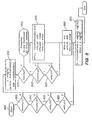
- FIG. 1 is a system level diagram showing the functional blocks of a system in accordance with an exemplary embodiment of the present invention.
- FIG. 2 is a matrix representation of a wide matrix multiply in accordance with an exemplary embodiment of the present invention.
- FIG. 3 is a further representation of a wide matrix multiple in accordance with an exemplary embodiment of the present invention.
- FIG. 4 is a system level diagram showing the functional blocks of a system incorporating a combined Simultaneous Multi Threading and Decoupled Access from Execution processor in accordance with an exemplary embodiment of the present invention.
- FIG. 5 illustrates a wide operand in accordance with an exemplary embodiment of the present invention.
- FIG. 6 illustrates an approach to specifier decoding in accordance with an exemplary embodiment of the present invention.
- FIG. 7 illustrates in operational block form a Wide Function Unit in accordance with an exemplary embodiment of the present invention.
- FIG. 8 illustrates in flow diagram form the Wide Microcache control function in accordance with an exemplary embodiment of the present invention.
- FIG. 9 illustrates Wide Microcache data structures in accordance with an exemplary embodiment of the present invention.
- FIGS. 10 and 11 illustrate a Wide Microcache control in accordance with an exemplary embodiment of the present invention.
- FIGS. 12A-12F illustrate a Wide Switch instruction in accordance with an exemplary embodiment of the present invention.
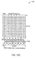
- FIGS. 13A-13G illustrate a Wide Translate instruction in accordance with an exemplary embodiment of the present invention.
- FIGS. 14A-14G illustrate a Wide Multiply Matrix instruction in accordance with an exemplary embodiment of the present invention.
- FIGS. 15A-15H illustrate a Wide Multiply Matrix Extract instruction in accordance with an exemplary embodiment of the present invention.
- FIGS. 16A-16G illustrate a Wide Multiply Matrix Extract Immediate instruction in accordance with an exemplary embodiment of the present invention.
- FIGS. 17A-17G illustrate a Wide Multiply Matrix Floating point instruction in accordance with an exemplary embodiment of the present invention.
- FIGS. 18A-18F illustrate a Wide Multiply Matrix Galois instruction in accordance with an exemplary embodiment of the present invention.
- FIGS. 19A-19H illustrate an Ensemble Extract Inplace instruction in accordance with an exemplary embodiment of the present invention.
- FIGS. 20A-20L illustrate an Ensemble Extract instruction in accordance with an exemplary embodiment of the present invention.
- FIGS. 21A-21H illustrate a System and Privileged Library Calls in accordance with an exemplary embodiment of the present invention.
- FIGS. 22A-22C illustrate an Ensemble Scale-Add Floating-point instruction in accordance with an exemplary embodiment of the present invention.
- FIGS. 23A-23E illustrate a Group Boolean instruction in accordance with an exemplary embodiment of the present invention.
- FIGS. 24A-24C illustrate a Branch Hint instruction in accordance with an exemplary embodiment of the present invention.
- FIGS. 25A-25C illustrate an Ensemble Sink Floating-point instruction in accordance with an exemplary embodiment of the present invention.
- FIGS. 26A-26E illustrate Group Add instructions in accordance with an exemplary embodiment of the present invention.
- FIGS. 27A-27E illustrate Group Set instructions and Group Subtract instructions in accordance with an exemplary embodiment of the present invention.
- FIGS. 28A-28K illustrate Ensemble Convolve, Ensemble Divide, Ensemble Multiply, and Ensemble Multiply Sum instructions in accordance with an exemplary embodiment of the present invention.
- FIG. 29 illustrates exemplary functions that are defined for use within the detailed instruction definitions in other sections.
- FIGS. 30A-30E illustrate Ensemble Floating-Point Add, Ensemble Floating-Point Divide, and Ensemble Floating-Point Multiply instructions in accordance with an exemplary embodiment of the present invention.
- FIGS. 31A-31C illustrate Ensemble Floating-Point Subtract instructions in accordance with an exemplary embodiment of the present invention.
- FIGS. 32A-32E illustrate Crossbar Compress, Expand, Rotate, and Shift instructions in accordance with an exemplary embodiment of the present invention.
- FIGS. 33A-33G illustrate Extract instructions in accordance with an exemplary embodiment of the present invention.
- FIGS. 34A-34H illustrate Shuffle instructions in accordance with an exemplary embodiment of the present invention.
- FIGS. 35A-35B illustrate Wide Solve Galois instructions in accordance with an exemplary embodiment of the present invention.
- FIGS. 36A-36B illustrate Wide Transform Slice instructions in accordance with an exemplary embodiment of the present invention.
- FIGS. 37A-37M illustrate Wide Convolve Extract instructions in accordance with an exemplary embodiment of the present invention.
- FIG. 38 illustrates Transfers Between Wide Operand Memories in accordance with an exemplary embodiment of the present invention.
- FIGS. 39A-39J illustrate operations in accordance with an exemplary embodiment of the present invention.
- FIGS. 40A-40C illustrate Instruction Fetch, Perform Exception, and Instruction Decode in accordance with an exemplary embodiment of the present invention.
- FIGS. 41A-41C illustrate a Always Reserved instruction in accordance with an exemplary embodiment of the present invention.
- FIGS. 42A-42C illustrate Address instructions in accordance with an exemplary embodiment of the present invention.
- FIGS. 43A-43C illustrate Address Compare instructions in accordance with an exemplary embodiment of the present invention.
- FIGS. 44A-44C illustrate Address Compare Floating Point instructions in accordance with an exemplary embodiment of the present invention.
- FIGS. 45A-45C illustrate Address Copy Immediate instructions in accordance with an exemplary embodiment of the present invention.
- FIGS. 46A-46C illustrate Address Immediate instructions in accordance with an exemplary embodiment of the present invention.
- FIGS. 47A-47C illustrate Address Immediate Reversed instructions in accordance with an exemplary embodiment of the present invention.
- FIGS. 48A-48C illustrate Address Immediate Set instructions in accordance with an exemplary embodiment of the present invention.
- FIGS. 49A-49C illustrate Address Reversed instructions in accordance with an exemplary embodiment of the present invention.
- FIGS. 50A-50C illustrate Address Set instructions in accordance with an exemplary embodiment of the present invention.
- FIGS. 51A-51C illustrate Address Set Floating Point instructions in accordance with an exemplary embodiment of the present invention.
- FIGS. 52A-52C illustrate an Address Shift Left Add instruction in accordance with an exemplary embodiment of the present invention.
- FIGS. 53A-53C illustrate an Address Shift Left Immediate Add instruction in accordance with an exemplary embodiment of the present invention.
- FIGS. 54A-54C illustrate Address Shift Immediate instructions in accordance with an exemplary embodiment of the present invention.
- FIGS. 55A-55C illustrate an Address Ternary instruction in accordance with an exemplary embodiment of the present invention.
- FIGS. 56A-56C illustrate a Branch instruction in accordance with an exemplary embodiment of the present invention.
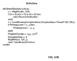
- FIGS. 57A-57C illustrate a Branch Back instruction in accordance with an exemplary embodiment of the present invention.
- FIGS. 58A-58C illustrate a Branch Barrier instruction in accordance with an exemplary embodiment of the present invention.
- FIGS. 59A-59C illustrate Branch Conditional instructions in accordance with an exemplary embodiment of the present invention.
- FIGS. 60A-60C illustrate Branch Conditional Floating-Point instructions in accordance with an exemplary embodiment of the present invention.
- FIGS. 61A-61C illustrate Branch Conditional Visibility Floating-Point instructions in accordance with an exemplary embodiment of the present invention.
- FIGS. 62A-62C illustrate a Branch Down instruction in accordance with an exemplary embodiment of the present invention.
- FIGS. 63A-63C illustrate a Branch Halt instruction in accordance with an exemplary embodiment of the present invention.
- FIGS. 64A-64C illustrate a Branch Hint Immediate instruction in accordance with an exemplary embodiment of the present invention.
- FIGS. 65A-65C illustrate a Branch Immediate instructions in accordance with an exemplary embodiment of the present invention.
- FIGS. 66A-66C illustrate a Branch Immediate Link instruction in accordance with an exemplary embodiment of the present invention.
- FIGS. 67A-67C illustrate a Branch Link instruction in accordance with an exemplary embodiment of the present invention.
- FIGS. 68A-68C illustrate Link instructions in accordance with an exemplary embodiment of the present invention.
- FIGS. 69A-69C illustrate Load Immediate instructions in accordance with an exemplary embodiment of the present invention.
- FIGS. 70A-70C illustrate Store instructions in accordance with an exemplary embodiment of the present invention.
- FIGS. 71A-71C illustrate Store Double Compare Swap instructions in accordance with an exemplary embodiment of the present invention.
- FIGS. 72A-72C illustrate Store Immediate instructions in accordance with an exemplary embodiment of the present invention.
- FIGS. 73A-73C illustrate Store Immediate Inplace instructions in accordance with an exemplary embodiment of the present invention.
- FIGS. 74A-74C illustrate Store Inplace instructions in accordance with an exemplary embodiment of the present invention.
- FIGS. 75A-75C illustrate Group Add Halve instructions in accordance with an exemplary embodiment of the present invention.
- FIGS. 76A-76C illustrate Group Compare instructions in accordance with an exemplary embodiment of the present invention.
- FIGS. 77A-77C illustrate Group Compare Floating-point instructions in accordance with an exemplary embodiment of the present invention.
- FIGS. 78A-78C illustrate Group Copy Immediate instructions in accordance with an exemplary embodiment of the present invention.
- FIGS. 79A-79C illustrate Group Immediate instructions in accordance with an exemplary embodiment of the present invention.
- FIGS. 80A-80C illustrate Group Immediate Reversed instructions in accordance with an exemplary embodiment of the present invention.
- FIGS. 81A-81C illustrate Group Inplace instructions in accordance with an exemplary embodiment of the present invention.
- FIGS. 82A-82C illustrate Group Reversed Floating-point instructions in accordance with an exemplary embodiment of the present invention.
- FIGS. 83A-83C illustrate Group Shift Left Immediate Add instructions in accordance with an exemplary embodiment of the present invention.
- FIGS. 84A-84C illustrate Group Shift Left Immediate Subtract instructions in accordance with an exemplary embodiment of the present invention.
- FIGS. 85A-85C illustrate Group Subtract Halve instructions in accordance with an exemplary embodiment of the present invention.
- FIGS. 86A-86C illustrate a Group Ternary instruction in accordance with an exemplary embodiment of the present invention.
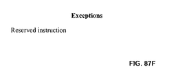
- FIGS. 87A-87F illustrate Crossbar Field instructions in accordance with an exemplary embodiment of the present invention.
- FIGS. 88A-88E illustrate Crossbar Field Inplace instructions in accordance with an exemplary embodiment of the present invention.
- FIGS. 89A-89C illustrate Crossbar Inplace instructions in accordance with an exemplary embodiment of the present invention.
- FIGS. 90A-90C illustrate Crossbar Short Immediate instructions in accordance with an exemplary embodiment of the present invention.
- FIGS. 91A-91C illustrate Crossbar Short Immediate Inplace instructions in accordance with an exemplary embodiment of the present invention.
- FIGS. 92A-92C illustrate a Crossbar Swizzle instruction in accordance with an exemplary embodiment of the present invention.
- FIGS. 93A-93D illustrate a Crossbar Ternary instruction in accordance with an exemplary embodiment of the present invention.
- FIGS. 94A-94G illustrate Ensemble Extract Immediate instructions in accordance with an exemplary embodiment of the present invention.
- FIGS. 95A-95I illustrate Ensemble Extract Immediate Inplace instructions in accordance with an exemplary embodiment of the present invention.
- FIGS. 96A-96E illustrate Ensemble Inplace Floating-point instructions in accordance with an exemplary embodiment of the present invention.
- FIGS. 97A-97D illustrate Ensemble Ternary instructions in accordance with an exemplary embodiment of the present invention.
- FIGS. 98A-98C illustrate Ensemble Unary instructions in accordance with an exemplary embodiment of the present invention.
- FIGS. 99A-99C illustrate Ensemble Unary Floating-point instructions in accordance with an exemplary embodiment of the present invention.
- FIG. 100 is a block diagram showing the organization of the memory management system in accordance with an exemplary embodiment of the present invention.
- FIG. 101 illustrates a pipeline organization in accordance with an exemplary embodiment of the present invention.
- FIG. 102 is a system-level diagram showing a memory pipeline in accordance with an exemplary embodiment of the present invention.
- FIG. 103 illustrates an expected rate at which memory requests are serviced in accordance with an exemplary embodiment of the present invention.
- FIG. 104 illustrates an expected rate at which memory requests are serviced in accordance with an exemplary embodiment of the present invention.
- FIG. 105 is a pinout diagram in accordance with an exemplary embodiment of the present invention.
- Micro Unity's Zeus Architecture describes general-purpose processor, memory, and interface subsystems, organized to operate at the enormously high bandwidth rates required for broadband applications.
- the Zeus processor performs integer, floating point, signal processing and non-linear operations such as Galois field, table lookup and bit switching on data sizes from 1 bit to 128 bits.
- Group or SIMD (single instruction multiple data) operations sustain external operand bandwidth rates up to 512 bits (i.e., up to four 128-bit operand groups) per instruction even on data items of small size.
- the processor performs ensemble operations such as convolution that maintain full intermediate precision with aggregate internal operand bandwidth rates up to 20,000 bits per instruction.
- the processor performs wide operations such as crossbar switch, matrix multiply and table lookup that use caches embedded in the execution units themselves to extend operands to as much as 32768 bits.
- All instructions produce at most a single 128-bit general register result, source at most three 128-bit general registers and are free of side effects such as the setting of condition codes and flags.
- the instruction set design carries the concept of streamlining beyond Reduced Instruction Set Computer (RISC) architectures, to simplify implementations that issue several instructions per machine cycle.
- RISC Reduced Instruction Set Computer
- the Zeus memory subsystem provides 64-bit virtual and physical addressing for UNIX, Mach, and other advanced OS environments. Separate address instructions enable the division of the processor into decoupled access and execution units, to reduce the effective latency of memory to the pipeline.
- the Zeus cache supplies the high data and instruction issue rates of the processor, and supports coherency primitives for scaleable multiprocessors.
- the memory subsystem includes mechanisms for sustaining high data rates not only in block transfer modes, but also in non-unit stride and scatterred access patterns.
- the Zeus interface subsystem is designed to match industry-standard protocols and pin-outs. In this way, Zeus can make use of existing infrastructure for building low-cost systems.
- the interface subsystem is modular, and can be replaced with appropriate protocols and pin-outs for lower-cost and higher-performance systems.
- the goal of the Zeus architecture is to integrate these processor, memory, and interface capabilities with optimal simplicity and generality. From the software perspective, the entire machine state consists of a program counter, a single bank of 64 general-purpose 128-bit general registers, and a linear byte-addressed shared memory space with mapped interface registers. All interrupts and exceptions are precise, and occur with low overhead.
- x + y two's complement addition of x and y. Result is the same size as the operands, and operands must be of equal size.
- x ⁇ y two's complement subtraction of y from x. Result is the same size as the operands, and operands must be of equal size.
- x * y two's complement multiplication of x and y. Result is the same size as the operands, and operands must be of equal size.
- x/y two's complement division of x by y. Result is the same size as the operands, and operands must be of equal size.
- Result is same size as the operands, and operands must be of equal size.
- y bitwise or of x and y. Result is same size as the operands, and operands must be of equal size.
- x ⁇ circumflex over ( ) ⁇ y bitwise exclusive- of x and y. Result is same size as the operands, and operands must be of equal size.
- ⁇ x bitwise inversion of x. Result is same size as the operand.
- x y two's complement equality comparison between x and y.
- Result is a single bit, and operands must be of equal size.
- Result is a single bit, and operands must be of equal size.
- Result is a single bit, and operands must be of equal size.
- Result is a single bit, and operands must be of equal size. ⁇ square root over (x) ⁇ floating-point square root of x x
- Result is a single bit.
- Value of x is a single bit.
- bits in this document is always little-endian, regardless of the ordering of bytes within larger data structures.
- the least-significant bit of a data structure is always labeled 0 (zero), and the most-significant bit is labeled as the data structure size (in bits) minus one.
- Zeus memory is an array of 264 bytes, without a specified byte ordering, which is physically distributed among various components.
- a byte is a single element of the memory array, consisting of 8 bits:
- a memory access of a data structure of size s at address i is formed from memory bytes at addresses i through i+s ⁇ 1.
- alignment it is not generally required that i be a multiple of s. Aligned accesses are preferred whenever possible, however, as they will often require one fewer processor or memory clock cycle than unaligned accesses.
- Zeus memory is byte-addressed, using either little-endian or big-endian byte ordering.
- Zeus uses little-endian byte ordering when an ordering must be selected.
- Zeus load and store instructions are available for both little-endian and big-endian byte ordering.
- the selection of byte ordering is dynamic, so that little-endian and big-endian processes, and even data structures within a process, can be intermixed on the processor.
- Zeus memory including memory-mapped registers, must conform to the following requirements regarding side-effects of read or load operations:
- a memory read must have no side-effects on the contents of the addressed memory nor on the contents of any other memory.
- Zeus memory including memory-mapped registers, must conform to the following requirements regarding side-effects of read or load operations:
- a memory write must affect the contents of the addressed memory so that a memory read of the addressed memory returns the value written, and so that a memory read of a portion of the addressed memory returns the appropriate portion of the value written.
- a memory write may affect or cause side-effects on the contents of memory not addressed by the write operation, however, a second memory write of the same value to the same address must have no side-effects on any memory; memory write operations must be idempotent.
- Zeus store instructions that are weakly ordered may have side-effects on the contents of memory not addressed by the store itself; subsequent load instructions which are also weakly ordered may or may not return values which reflect the side-effects.
- Zeus provides eight-byte (64-bit) virtual and physical address sizes, and eight-byte (64-bit) and sixteen-byte (128-bit) data path sizes, and uses fixed-length four-byte (32-bit) instructions. Arithmetic is performed on two's-complement or unsigned binary and ANSI/IEEE standard 754-1985 conforming binary floating-point number representations.
- a bit is a primitive data element:
- a peck is the catenation of two bits:
- a nibble is the catenation of four bits:
- a byte is the catenation of eight bits, and is a single element of the memory array:
- a doublet is the catenation of 16 bits, and is the catenation of two bytes:
- a quadlet is the catenation of 32 bits, and is the catenation of four bytes:
- An octlet is the catenation of 64 bits, and is the catenation of eight bytes:
- a hexlet is the catenation of 128 bits, and is the catenation of sixteen bytes:
- a triclet is the catenation of 256 bits, and is the catenation of thirty-two bytes:
- Zeus addresses both virtual addresses and physical addresses, are octlet quantities.
- Zeus's floating-point formats are designed to satisfy ANSI/IEEE standard 754-1985: Binary Floating-point Arithmetic. Standard 754 leaves certain aspects to the discretion of implementers: additional precision formats, encoding of quiet and signaling NaN values, details of production and propagation of quiet NaN values. These aspects are detailed below.
- Zeus adds additional half-precision and quad-precision formats to standard 754's single-precision and double-precision formats.
- Zeus's double-precision satisfies standard 754's precision requirements for a single-extended format
- Zeus's quad-precision satisfies standard 754's precision requirements for a double-extended format.
- Each precision format employs fields labeled s (sign), e (exponent), and f (fraction) to encode values that are (1) NaN: quiet and signaling, (2) infinities: ( ⁇ 1) ⁇ s ⁇ , (3) normalized numbers: ( ⁇ 1) ⁇ s 2 ⁇ e-bias (1.f), (4) denormalized numbers: ( ⁇ 1) ⁇ s 2 ⁇ 1-bias (0.f), and (5) zero: ( ⁇ 1) ⁇ s 0.
- Quiet NaN values are denoted by any sign bit value, an exponent field of all one bits, and a non-zero fraction with the most significant bit set.
- Quiet NaN values generated by default exception handling of standard operations have a zero sign bit, an exponent field of all one bits, a fraction field with the most significant bit set, and all other bits cleared.
- Signaling NaN values are denoted by any sign bit value, an exponent field of all one bits, and a non-zero fraction with the most significant bit cleared.
- Infinite values are denoted by any sign bit value, an exponent field of all one bits, and a zero fraction field.
- Normalized number values are denoted by any sign bit value, an exponent field that is not all one bits or all zero bits, and any fraction field value.
- the numeric value encoded is ( ⁇ 1) ⁇ s 2 ⁇ e-bias (1.f).
- the bias is equal the value resulting from setting all but the most significant bit of the exponent field, half: 15, single: 127, double: 1023, and quad: 16383.
- Denormalized number values are denoted by any sign bit value, an exponent field that is all zero bits, and a non-zero fraction field value.
- the numeric value encoded is ( ⁇ 1) ⁇ s 2 ⁇ 1-bias (0.f).
- Zero values are denoted by any sign bit value, and exponent field that is all zero bits, and a fraction field that is all zero bits.
- the numeric value encoded is ( ⁇ 1) ⁇ s 0. The distinction between +0 and ⁇ 0 is significant in some operations.
- Zeus half precision uses a format similar to standard 754's requirements, reduced to a 16-bit overall format.
- the format contains sufficient precision and exponent range to hold a 12-bit signed integer.
- Zeus quad precision satisfies standard 754's requirements for “double extended,” but has additional fraction precision to use 128 bits.
- Zeus instructions include operations on pairs of data values that represent complex numerical values of the form (a+b i). When contained in general registers, the paired values are always arranged with the real part (a) in a less-significant location (to the right) and the imaginary part (b i) in a more-significant location (to the left).
- a little-endian load or store transfers these values to memory in a form where the real part is at a lower address and the imaginary part is at a higher address.
- a big-endian load or store transfers these values to memory in a form where the real part is at a higher address and the imaginary part is at a lower address, which is different from the little-endian case and may be considered unusual.
- an X.SWIZZLE instruction can swap the positions of the real and imaginary values in a general register for the operands and the results.
- a shortcut for a complex multiply operation can be observed: if the position of the real and imaginary parts are reversed in both operands, the result that is computed will have the imaginary part of the result to the left (more significant) and the negative of the real part to the right (less significant).
- a G.XOR can invert the sign bit (for complex floating-point), or the real part of the result (for complex integer).
- a G.ADD then transforms the ones-complement to a twos-complement.
- An X.SWIZZLE instruction can swap the result into the reversed order matching the operand order. The results transformed by the above is then in condition to be written back to memory in the reversed fashion.
- the Zeus system architecture reaches above the processor level architecture.
- Optional areas include:
- Additional devices and interfaces may be added in specified regions of the physical memory space, provided that system reset places these devices and interfaces in an inactive state that does not interfere with the operation of software that runs in any conformant system.
- the software interface requirements of any such additional devices and interfaces must be made as widely available as this architecture specification.
- a computer system may conform to the Zeus System Architecture while employing any number of components, dissipate any amount of heat, require any special environmental facilities, or be of any physical size.
- MicroUnity's Zeus processor provides the general-purpose, high-bandwidth computation capability of the Zeus system.
- Zeus includes high-bandwidth data paths, general register files, and a memory hierarchy.
- Zeus's memory hierarchy includes on-chip instruction and data memories, instruction and data caches, a virtual memory facility, and interfaces to external devices.
- Zeus's interfaces in the initial implementation are solely the “Super Socket 7” bus, but other implementations may have different or additional interfaces.
- the Zeus architecture defines a compatible framework for a family of implementations with a range of capabilities.
- the following implementation-defined parameters are used in the rest of the document in boldface. The value indicated is for one implementation.
- the first implementation of Zeus uses “socket 7” protocols and pinouts.
- Instructions are specified to Zeus assemblers and other code tools (assemblers) in the syntax of an instruction mnemonic (operation code), then optionally white space (blanks or tabs) followed by a list of operands.
- instruction mnemonics listed in this specification are in upper case (capital) letters, assemblers accept either upper case or lower case letters in the instruction mnemonics.
- instruction mnemonics contain periods (“.”) to separate elements to make them easier to understand; assemblers ignore periods within instruction mnemonics.
- the instruction mnemonics are designed to be parsed uniquely without the separating periods.
- the result and source operands are case-sensitive; upper case and lower case letters are distinct.
- General register operands are specified by the names r0 (or r00) through r63 (a lower case “r” immediately followed by a one or two digit number from 0 to 63), or by the special designations of “lp” for “r0,” “dp” for “r1,” “fp” for “r62,” and “sp” for “r63.”
- Integer-valued operands are specified by an optional sign ( ⁇ ) or (+) followed by a number, and assemblers generally accept a variety of integer-valued expressions.
- a Zeus instruction is specifically defined as a four-byte structure with the little-endian ordering shown below. It is different from the quadlet defined above because the placement of instructions into memory must be independent of the byte ordering used for data structures. Instructions must be aligned on four-byte boundaries; in the diagram below, i must be a multiple of 4.
- a Zeus gateway is specifically defined as an 8-byte structure with the little-endian ordering shown below.
- a gateway contains a code address used to securely invoke a system call or procedure at a higher privilege level. Gateways are marked by protection information specified in the TB. Gateways must be aligned on 8-byte boundaries; in the diagram below, i must be a multiple of 8.
- the gateway contains two data items within its structure, a code address and a new privilege level:
- the virtual memory system can be used to designate a region of memory as containing gateways.
- Other data may be placed within the gateway region, provided that if an attempt is made to use the additional data as a gateway, that security cannot be violated.
- the user state consists of hardware data structures that are accessible to all conventional compiled code.
- the Zeus user state is designed to be as regular as possible, and consists only of the general registers, the program counter, and virtual memory. There are no specialized registers for condition codes, operating modes, rounding modes, integer multiply/divide, or floating-point values.
- Zeus user state includes 64 general registers. All are identical; there is no dedicated zero-valued general register, and there are no dedicated floating-point general registers.
- Some Zeus instructions have 32-bit or 64-bit general register operands. These operands are sign-extended to 128 bits when written to the general register file, and the low-order bits are chosen when read from the general register file.
- the program counter contains the address of the currently executing instruction. This register is implicitly manipulated by branch instructions, and read by branch instructions that save a return address in a general register.
- the privilege level register contains the privilege level of the currently executing instruction. This register is implicitly manipulated by branch gateway and branch down instructions, and read by branch gateway instructions that save a return address in a general register.
- the program counter and privilege level may be packed into a single octlet. This combined data structure is saved by the Branch Gateway instruction and restored by the Branch Down instruction.
- System State The system state consists of the facilities not normally used by conventional compiled code. These facilities provide mechanisms to execute such code in a fully virtual environment. All system state is memory mapped, so that it can be manipulated by compiled code.
- Zeus provides load and store instructions to move data between memory and the general registers, branch instructions to compare the contents of general registers and to transfer control from one code address to another, and arithmetic operations to perform computation on the contents of general registers, returning the result to general registers.
- the load and store instructions move data between memory and the general registers.
- values are zero-extended or sign-extended to fill the general register.
- values are truncated on the left to fit the specified memory region.
- Load and store instructions that specify a memory region of more than one byte may use either little-endian or big-endian byte ordering: the size and ordering are explicitly specified in the instruction. Regions larger than one byte may be either aligned to addresses that are an even multiple of the size of the region or of unspecified alignment: alignment checking is also explicitly specified in the instruction.
- Load and store instructions specify memory addresses as the sum of a base general register and the product of the size of the memory region and either an immediate value or another general register. Scaling maximizes the memory space which can be reached by immediate offsets from a single base general register, and assists in generating memory addresses within iterative loops. Alignment of the address can be reduced to checking the alignment of the first general register.
- the load and store instructions are used for fixed-point data as well as floating-point and digital signal processing data; Zeus has a single bank of general registers for all data types.
- Swap instructions provide multithread and multiprocessor synchronization, using indivisible operations: add-swap, compare-swap, multiplex-swap, and double-compare-swap.
- a store-multiplex operation provides the ability to indivisibly write to a portion of an octlet. These instructions always operate on aligned octlet data, using either little-endian or big-endian byte ordering.
- the fixed-point compare-and-branch instructions provide all arithmetic tests for equality and inequality of signed and unsigned fixed-point values. Tests are performed either between two operands contained in general registers, or on the bitwise and of two operands. Depending on the result of the compare, either a branch is taken, or not taken. A taken branch causes an immediate transfer of the program counter to the target of the branch, specified by a 12-bit signed offset from the location of the branch instruction. A non-taken branch causes no transfer; execution continues with the following instruction.
- branch instructions provide for unconditional transfer of control to addresses too distant to be reached by a 12-bit offset, and to transfer to a target while placing the location following the branch into a general register.
- the branch through gateway instruction provides a secure means to access code at a higher privilege level, in a form similar to a normal procedure call.
- a subset of general fixed-point arithmetic operations is available as addressing operations. These include add, subtract, Boolean, and simple shift operations. These addressing operations may be performed at a point in the Zeus processor pipeline so that they may be completed prior to or in conjunction with the execution of load and store operations in a “superspring” pipeline in which other arithmetic operations are deferred until the completion of load and store operations.
- DSP Digital Signal Processing
- These operations perform arithmetic operations on values of 8-, 16-, 32-, 64-, or 128-bit sizes, which are right-aligned in general registers.
- These execution operations include the add, subtract, boolean and simple shift operations which are also available as addressing operations, but further extend the available set to include three-operand add/subtract, three-operand boolean, dynamic shifts, and bit-field operations.
- Zeus provides all the facilities mandated and recommended by ANSI/IEEE standard 754-1985: Binary Floating-point Arithmetic, with the use of supporting software.
- the floating-point compare-and-branch instructions provide all the comparison types required and suggested by the IEEE floating-point standard. These floating-point comparisons augment the usual types of numeric value comparisons with special handling for NaN (not-a-number) values. A NaN value compares as “unordered” with respect to any other value, even that of an identical NaN value.
- Zeus floating-point compare-branch instructions do not generate an exception on comparisons involving quiet or signaling NaN values. If such exceptions are desired, they can be obtained by combining the use of a floating-point compare-set instruction, with either a floating-point compare-branch instruction on the floating-point operands or a fixed-point compare-branch on the set result.
- the E relation can be used to determine the unordered condition of a single operand by comparing the operand with itself.
- compare-set floating-point instructions provide all the comparison types supported as branch instructions. Zeus compare-set floating-point instructions may optionally generate an exception on comparisons involving quiet or signaling NaNs.
- the basic operations supported in hardware are floating-point add, subtract, multiply, divide, square root and conversions among floating-point formats and between floating-point and binary integer formats.
- the operations explicitly specify the precision of the operation, and round the result (or check that the result is exact) to the specified precision at the conclusion of each operation.
- Each of the basic operations splits operand general registers into symbols of the specified precision and performs the same operation on corresponding symbols.
- Zeus performs a variety of operations in which one or more products are summed to each other and/or to an additional operand.
- the instructions include a fused multiply-add (E.MUL.ADD.F), convolve (E.CON.F), matrix multiply (E.MUL.MAT.F), and scale-add (E.SCAL.ADD.F).
- Rounding is specified within the instructions explicitly, to avoid explicit state registers for a rounding mode.
- the instructions explicitly specify how standard exceptions (invalid operation, division by zero, overflow, underflow and inexact) are to be handled (U.S. Pat. No. 5,812,439 describes this “Technique of incorporating floating point information into processor instructions.”).
- This technique assists the Zeus processor in executing floating-point operations with greater parallelism.
- Zeus may safely retire instructions following them, as they are guaranteed not to cause data-dependent exceptions.
- floating-point instructions with N, Z, F, or C control can be guaranteed not to cause data-dependent exceptions once the operands have been examined to rule out invalid operations, division by zero, overflow or underflow exceptions.
- Only floating-point instructions with X control, or when exceptions cannot be ruled out with N, Z, F, or C control need to avoid retiring following instructions until the final result is generated.
- ANSI/IEEE standard 754-1985 specifies information to be given to trap handlers for the five floating-point exceptions.
- the Zeus architecture produces a precise exception, (The program counter points to the instruction that caused the exception and all general register state is present) from which all the required information can be produced in software, as all source operand values and the specified operation are available.
- ANSI/IEEE standard 754-1985 specifies a set of five “sticky-exception” bits, for recording the occurrence of exceptions that are handled by default.
- the Zeus architecture produces a precise exception for instructions with N, Z, F, or C control for invalid operation, division by zero, overflow or underflow exceptions and with X control for all floating-point exceptions, from which software may arrange that corresponding sticky-exception bits can be set.
- Execution of the same instruction with default control will compute the default result with round-to-nearest rounding.
- Most compound operations not specified by the standard are not available with rounding and exception controls. These compound operations provide round-to-nearest rounding and default exception handling.
- ANSI/IEEE standard 754-1985 specifies that operations involving a signaling NaN or invalid operation shall, if no trap occurs and if a floating-point result is to be delivered, deliver a quiet NaN as its result. However, it fails to specify what quiet NaN value to deliver.
- Zeus operations that produce a floating-point result and do not trap on invalid operations propagate signaling NaN values from operands to results, changing the signaling NaN values to quiet NaN values by setting the most significant fraction bit and leaving the remaining bits unchanged.
- Other causes of invalid operations produce the default quiet NaN value, where the sign bit is zero, the exponent field is all one bits, the most significant fraction bit is set and the remaining fraction bits are zero bits.
- signaling NaN propagation or quiet NaN production is handled separately and independently for each result symbol.
- ANSI/IEEE standard 754-1985 specifies that quiet NaN values should be propagated from operand to result by the basic operations. However, it fails to specify which of several quiet NaN values to propagate when more than one operand is a quiet NaN. In addition, the standard does not clearly specify how quiet NaN should be propagated for the multiple-operation instructions provided in Zeus. The standard does not specify the quiet NaN produced as a result of an operand being a signaling NaN when invalid operation exceptions are handled by default. The standard leaves unspecified how quiet and signaling NaN values are propagated though format conversions and the absolute-value, negate and copy operations. This section specifies these aspects left unspecified by the standard.
- quiet and signaling NaN propagation is handled separately and independently for each result symbol.
- a quiet or signaling NaN value in a single symbol of an operand causes only those result symbols that are dependent on that operand symbol's value to be propagated as that quiet NaN.
- Multiple quiet or signaling NaN values in symbols of an operand which influence separate symbols of the result are propagated independently of each other. Any signaling NaN that is propagated has the high-order fraction bit set to convert it to a quiet NaN.
- Priority shall be given to the operand that is specified by a general register definition at a lower-numbered (little-endian) bit position within the instruction (rb has priority over rc, which has priority over rd). In the case of operands which are catenated from two general registers, priority shall be assigned based on the general register which has highest priority (lower-numbered bit position within the instruction).
- the value which is located at a lower-numbered (little-endian) bit position within the operand is to receive priority.
- the identification of a NaN as quiet or signaling shall not confer any priority for selection—only the operand position, though a signaling NaN will cause an invalid operand exception.
- the sign bit of NaN values propagated shall be complemented if the instruction subtracts or negates the corresponding operand or (but not and) multiplies it by or divides it by or divides it into an operand which has the sign bit set, even if that operand is another NaN. If a NaN is both subtracted and multiplied by a negative value, the sign bit shall be propagated unchanged.
- NaN values are propagated by preserving the sign and the most-significant fraction bits, except that the most-significant bit of a signalling NaN is set and (for DEFLATE) the least-significant fraction bit preserved is combined, via a logical—or of all fraction bits not preserved. All additional fraction bits (for INFLATE) are set to zero.
- NaN values For Zeus operations that convert from a floating-point format to a fixed-point format (SINK), NaN values produce zero values (maximum-likelihood estimate). Infinity values produce the largest representable positive or negative fixed-point value that fits in the destination field. When exception traps are enabled, NaN or Infinity values produce a floating-point exception. Underflows do not occur in the SINK operation, they produce ⁇ 1, 0 or +1, depending on rounding controls.
- NaN values are propagated with the sign bit cleared, complemented, or copied, respectively.
- Signalling NaN values cause the Invalid operation exception, propagating a quieted NaN in corresponding symbol locations (default) or an exception, as specified by the instruction.
- ANSI/IEEE standard 754-1985 specifies that invalid operation shall be signaled if an operand is invalid for the operation to be performed. Zeus operations that specify a rounding mode trap on invalid operation. Zeus operations that default the rounding mode (to round to nearest) do not trap on invalid operation and produce a quiet NaN result as described above.
- Standard compliant software produces the required result to a trap handler by following the requirements of the standard.
- Software may simulate untrapped invalid operation for other specified rounding modes by following the requirements of the standard for the result.
- ANSI/IEEE standard 754-1985 specifies that division by zero shall be signaled the divisor is zero and the dividend is a finite non zero number. Zeus operations that specify a rounding mode trap on division by zero. Zeus operations that default the rounding mode (to round to nearest) do not trap on division by zero and produce a signed infinity result.
- Standard compliant software produces the required result to a trap handler by following the requirements of the standard.
- Software may simulate untrapped division by zero for other specified rounding modes by following the requirements of the standard for the result.
- ANSI/IEEE standard 754-1985 specifies that overflow shall be signaled whenever the destination format's largest finite number is exceeded in magnitude by what would have been the rounded floating-point result were the exponent range unbounded.
- Zeus operations that specify a rounding mode trap on overflow Zeus operations that default the rounding mode (to round to nearest) do not trap on overflow and produce a result that carries all overflows to infinity with the sign of the intermediate result.
- Standard compliant software produces the required result to a trap handler by following the requirements of the standard.
- Software may simulate untrapped overflow for other specified rounding modes by following the requirements of the standard for the result.
- the standard specifies a value with the sign of the intermediate result and specifies the largest finite number when the overflow is in the direction away from rounding or infinity otherwise.
- ANSI/IEEE standard 754-1985 specifies that underflow is dependent on two correlated events: tininess and loss of accuracy, but allows some latitude in the definition of these conditions.
- tininess is detected “after rounding,” that is when a non zero result computed as though the exponent range were unbounded would lie between the smallest normalized number for the format of the result.
- Zeus hardware does not produce sticky exception bits, so a notion of loss of accuracy does not apply.
- Standard compliant software produces the required result to a trap handler by following the requirements of the standard.
- Software may simulate untrapped underflow sticky exceptions by using the trapping operations and simulating a result, applying whatever definition of loss of accuracy is desired.
- ANSI/IEEE standard 754-1985 specifies that inexact shall be signaled whenever the rounded result of an operation is not exact or if it overflows without an overflow trap.
- Zeus operations that specify “exact” rounding trap on inexact Zeus operations that default the rounding mode (to round to nearest) or specify a rounding mode do not trap on inexact and produce a rounded or overflowed result.
- Standard compliant software produces the required result to a trap handler by following the requirements of the standard, delivering a rounded result.
- an internal format represents infinite-precision floating-point values as a four-element structure consisting of (1) s (sign bit): 0 for positive, 1 for negative, (2) t (type): NORM, ZERO, SNAN, QNAN, INFINITY, (3) e (exponent), and (4) f: (fraction).
- the mathematical interpretation of a normal value places the binary point at the units of the fraction, adjusted by the exponent: ( ⁇ 1) ⁇ s *(2 ⁇ e )*f.
- the function F converts a packed IEEE floating-point value into internal format.
- the function PackF converts an internal format back into IEEE floating-point format, with rounding and exception control.
- the Zeus processor provides a set of operations that maintain the fullest possible use of 128-bit data paths when operating on lower-precision fixed-point or floating-point vector values. These operations are useful for several application areas, including digital signal processing, image processing and synthetic graphics. The basic goal of these operations is to accelerate the performance of algorithms that exhibit the following characteristics:
- operands and intermediate results are fixed-point values represented in no greater than 64 bit precision.
- operands and intermediate results are of 16, 32, or 64 bit precision.
- the fixed-point arithmetic operations include add, subtract, multiply, divide, shifts, and set on compare.
- fixed-point arithmetic permits various forms of operation reordering that are not permitted in floating-point arithmetic. Specifically, commutativity and associativity, and distribution identities can be used to reorder operations. Compilers can evaluate operations to determine what intermediate precision is required to get the specified arithmetic result.
- Zeus supports several levels of precision, as well as operations to convert between these different levels. These precision levels are always powers of two, and are explicitly specified in the operation code.
- add, subtract, and shift operations may cause a fixed-point arithmetic exception to occur on resulting conditions such as signed or unsigned overflow.
- the fixed-point arithmetic exception may also be invoked upon a signed or unsigned comparison.
- the algorithms are or can be expressed as operations on sequentially ordered items in memory. Scatter-gather memory access or sparse-matrix techniques are not required.
- nx+k the value of n must be a power of two, and the values referenced should have k include the majority of values in the range 0 . . . n ⁇ 1.
- a negative multiplier may also be used.
- two hexlet general registers specify the source triclet, and one of the two result hexlets are specified as hexlet general register.
- n is 2.
- shuffle operations can be used to further subdivide the sequential stream. For example, when n is 4, we need to deal out 4 sets of doublet operands, as shown in FIG. 39C .
- a four-way deal is a digital signal processing application such as conversion of color to monochrome.
- the reverse of the “deal” operation needs to be performed on vectors of results to interleave them for storage in sequential order.
- the “shuffle” operation interleaves the bit fields of two octlets of results into a single hexlet. For example a X.SHUFFLE.16 operation combines two octlets of doublet fields into a hexlet as in FIG. 39D .
- a series of shuffle operations can be used to combine additional sets of fields, similarly to the mechanism used for the deal operations. For example, when n is 4, we need to shuffle up 4 sets of doublet operands, as shown in FIG. 39E .
- a four-way shuffle is a digital signal processing application such as conversion of monochrome to color.
- nx+k When the index of a source array operand or a destination array result is negated, or in other words, if of the form nx+k where n is negative, the elements of the array must be arranged in reverse order.
- a group instruction in which one or more operands is a single value, not an array.
- the “swizzle” operation can also copy operands to multiple locations within a hexlet. For example, a X.SWIZZLE 15,0 operation copies the low-order 16 bits to each double within a hexlet.
- Variations of the deal and shuffle operations are also useful for converting from one precision to another. This may be required if one operand is represented in a different precision than another operand or the result, or if computation must be performed with intermediate precision greater than that of the operands, such as when using an integer multiply.
- the “compress” operation is a variant of the “deal” operation, in which the operand is a hexlet, and the result is an octlet.
- m is the precision of the source operand.
- An operand can be doubled in precision and shifted left with the “expand” operation, which is essentially the reverse of the “compress” operation.
- the “shuffle” operation can double the precision of an operand and multiply it by 1 (unsigned only), 2 m or 2 m +1, by specifying the sources of the shuffle operation to be a zeroed general register and the source operand, the source operand and zero, or both to be the source operand.
- a constant can be freely added to the source operand by specifying the constant as the right operand to the shuffle.
- the characteristics of the algorithms that affect the arithmetic operations most directly are low-precision arithmetic, and vectorizable operations.
- the fixed-point arithmetic operations provided are most of the functions provided in the standard integer unit, except for those that check conditions. These functions include add, subtract, bitwise Boolean operations, shift, set on condition, and multiply, in forms that take packed sets of bit fields of a specified size as operands.
- the floating-point arithmetic operations provided are as complete as the scalar floating-point arithmetic set. The result is generally a packed set of bit fields of the same size as the operands, except that the fixed-point multiply function intrinsically doubles the precision of the bit field.
- Conditional operations are provided only in the sense that the set on condition operations can be used to construct bit masks that can select between alternate vector expressions, using the bitwise Boolean operations. All instructions operate over the entire octlet or hexlet operands, and produce a hexlet result. The sizes of the bit fields supported are always powers of two.
- Zeus provides a general software solution to the most common operations required for Galois Field arithmetic.
- the instructions provided include a polynomial multiply, with the polynomial specified as one general register operand. This instruction can be used to perform CRC generation and checking, Reed-Solomon code generation and checking, and spread-spectrum encoding and decoding.
- general registers are saved either by the caller or callee procedure, which provides a mechanism for leaf procedures to avoid needing to save general registers.
- Compilers may choose to allocate variables into caller or callee saved general registers depending on how their lifetimes overlap with procedure calls.
- Procedure parameters are normally allocated in general registers, starting from general register 2 up to general register 9. These general registers hold up to 8 parameters, which may each be of any size from one byte to sixteen bytes (hexlet), including floating-point and small structure parameters. Additional parameters are passed in memory, allocated on the stack. For C procedures which use varargs.h or stdarg.h and pass parameters to further procedures, the compilers must leave room in the stack memory allocation to save general registers 2 through 9 into memory contiguously with the additional stack memory parameters, so that procedures such as _doprnt can refer to the parameters as an array.
- Procedure return values are also allocated in general registers, starting from general register 2 up to general register 9. Larger values are passed in memory, allocated on the stack.
- the lp general register contains the address to which the callee should return to at the conclusion of the procedure. If the procedure is also a caller, the lp general register will need to be saved on the stack, once, before any procedure call, and restored, once, after all procedure calls. The procedure returns with a branch instruction, specifying the lp general register.
- the sp general register is used to form addresses to save parameter and other general registers, maintain local variables, i.e., data that is allocated as a LIFO stack. For procedures that require a stack, normally a single allocation is performed, which allocates space for input parameters, local variables, saved general registers, and output parameters all at once.
- the sp general register is always hexlet aligned.
- the dp general register is used to address pointers, literals and static variables for the procedure.
- the dp general register points to a small (approximately 4096-entry) array of pointers, literals, and statically-allocated variables, which is used locally to the procedure.
- the uses of the dp general register are similar to the use of the gp general register on a Mips R-series processor, except that each procedure may have a different value, which expands the space addressable by small offsets from this pointer. This is an important distinction, as the offset field of Zeus load and store instructions are only 12 bits.
- the compiler may use additional general registers and/or indirect pointers to address larger regions for a single procedure.
- the compiler may also share a single dp general register value between procedures which are compiled as a single unit (including procedures which are externally callable), eliminating the need to save, modify and restore the dp general register for calls between procedures which share the same dp general register value.
- Load- and store-immediate-aligned instructions specifying the dp general register as the base general register, are generally used to obtain values from the dp region. These instructions shift the immediate value by the logarithm of the size of the operand, so loads and stores of large operands may reach farther from the dp general register than of small operands.
- the size of the addressable region is maximized if the elements to be placed in the dp region are sorted according to size, with the smallest elements placed closest to the dp base. At points where the size changes, appropriate padding is added to keep elements aligned to memory boundaries matching the size of the elements. Using this technique, the maximum size of the dp region is always at least 4096 items, and may be larger when the dp area is composed of a mixture of data sizes.
- the dp general register mechanism also permits code to be shared, with each static instance of the dp region assigned to a different address in memory. In conjunction with position-independent or pc-relative branches, this allows library code to be dynamically relocated and shared between processes.
- the lp general register is loaded with the entry point of the procedure, and the dp general register is loaded with the value of the dp general register required for the procedure. These two values are located adjacent to each other as a pair of octlet quantities in the dp region for the calling procedure.
- the linker fills in the values at link time.
- this mechanism also provides for dynamic linking, by initially filling in the lp and dp fields in the data structure to invoke the dynamic linker.
- the dynamic linker can use the contents of the lp and/or dp general registers to determine the identity of the caller and callee, to find the location to fill in the pointers and resume execution.
- the lp value is initially set to point to an entry point in the dynamic linker
- the dp value is set to point to itself: the location of the lp and dp values in the dp region of the calling procedure.
- the identity of the procedure can be discovered from a string following the dp pointer, or a separate table, indexed by the dp pointer.
- the fp general register is used to address the stack frame when the stack size varies during execution of a procedure, such as when using the GNU C alloca function.
- the sp general register is used to address the stack frame and the fp general register may be used for any other general purpose as a callee-saved general register.
- Procedures that are compiled together may share a common data region, in which case there is no need to save, load, and restore the dp region in the callee, assuming that the callee does not modify the dp general register.
- the pc-relative addressing of the B.LINK.I instruction permits the code region to be position-independent.
- the stack frame may also be eliminated from the caller procedure by using “temporary” caller save general registers not utilized by the callee leaf procedures.
- this usage may include other values and variables that live in the caller procedure across callee procedure calls.
- the load instruction is required in the caller following the procedure call to restore the dp general register.
- a second load instruction also restores the lp general register, which may be located at any point between the last procedure call and the branch instruction which returns from the procedure.
- Such a procedure must not be entered from anywhere other than its legitimate entry point, to prohibit entering a procedure after the point at which security checks are performed or with invalid general register contents, otherwise the access to a higher privilege level can lead to a security violation.
- the procedure generally must have access to memory data, for which addresses must be produced by the privileged code.
- the branch-gateway instruction allows the privileged code procedure to rely the fact that a single general register has been verified to contain a pointer to a valid memory region.
- the branch-gateway instruction ensures both that the procedure is invoked at a proper entry point, and that other general registers such as the data pointer and stack pointer can be properly set. To ensure this, the branch-gateway instruction retrieves a “gateway” directly from the protected virtual memory space.
- the gateway contains the virtual address of the entry point of the procedure and the target privilege level.
- a gateway can only exist in regions of the virtual address space designated to contain them, and can only be used to access privilege levels at or below the privilege level at which the memory region can be written to ensure that a gateway cannot be forged.
- the branch-gateway instruction ensures that general register 1 (dp) contains a valid pointer to the gateway for this target code address by comparing the contents of general register 0 (lp) against the gateway retrieved from memory and causing an exception trap if they do not match.
- auxiliary information such as the data pointer and stack pointer can be set by loading values located by the contents of general register 1. For example, the eight bytes following the gateway may be used as a pointer to a data region for the procedure.
- general register 1 must be set to point at the gateway, and general register 0 must be set to the address of the target code address plus the desired privilege level.
- a return from a system or privileged routine involves a reduction of privilege. This need not be carefully controlled by architectural facilities, so a procedure may freely branch to a less-privileged code address. Normally, such a procedure restores the stack frame, then uses the branch-down instruction to return.
- the calling sequence is identical to that of the inter-module calling sequence shown above, except for the use of the B.GATE instruction instead of a B.LINK instruction. Indeed, if a B.GATE instruction is used when the privilege level in the lp general register is not higher than the current privilege level, the B.GATE instruction performs an identical function to a B.LINK.
- the callee if it uses a stack for local variable allocation, cannot necessarily trust the value of the sp passed to it, as it can be forged. Similarly, any pointers which the callee provides should not be used directly unless it they are verified to point to regions which the callee should be permitted to address. This can be avoided by defining application programming interfaces (APIs) in which all values are passed and returned in general registers, or by using a trusted, intermediate privilege wrapper routine to pass and return parameters. The method described below can also be used.
- APIs application programming interfaces
- a user may request that errors in a privileged routine be reported by invoking a user-supplied error-logging routine.
- the privilege can be reduced via the branch-down instruction.
- the return from the procedure actually requires an increase in privilege, which must be carefully controlled. This is dealt with by placing the procedure call within a lower-privilege procedure wrapper, which uses the branch-gateway instruction to return to the higher privilege region after the call through a secure re-entry point.
- FIG. 1 a general purpose processor is illustrated therein in block diagram form.
- the general purpose processor operates under control of a stored computer program.
- FIG. 1 four copies of an access unit are shown, each with an access instruction fetch queue A-Queue 101 - 104 .
- Each access instruction fetch queue A-Queue 101 - 104 is coupled to an access register file AR 105 - 108 , which are each coupled to two access functional units A 109 - 116 .
- each thread of the processor may have on the order of sixty-four general purpose registers (e.g., the AR's 105 - 108 and ER's 125 - 128 ).
- the access units function independently for four simultaneous threads of execution, and each compute program control flow by performing arithmetic and branch instructions and access memory by performing load and store instructions. These access units also provide wide operand specifiers for wide operand instructions. These eight access functional units A 109 - 116 produce results for access register files AR 105 - 108 and memory addresses to a shared memory system 117 - 120 .
- the memory hierarchy includes on-chip instruction and data memories, instruction and data caches, a virtual memory facility, and interfaces to external devices.
- the memory system is comprised of a combined cache and niche memory 117 , an external bus interface 118 , and, externally to the device, a secondary cache 119 and main memory system with I/O devices 120 .
- the memory contents fetched from memory system 117 - 120 are combined with execute instructions not performed by the access unit, and entered into the four execute instruction queues E-Queue 121 - 124 .
- memory contents fetched from memory system 117 - 120 are also provided to wide operand microcaches 132 - 136 by bus 137 .
- Instructions and memory data from E-queue 121 - 124 are presented to execution register files 125 - 128 , which fetch execution register file source operands.
- the instructions are coupled to the execution unit arbitration unit Arbitration 131 , that selects which instructions from the four threads are to be routed to the available execution functional units E 141 and 149 , X 142 and 148 , G 143 - 144 and 146 - 147 , and T 145 .
- the execution functional units E 141 and 149 , the execution functional units X 142 and 148 , and the execution functional unit T 145 each contain a wide operand microcache 132 - 136 , which are each coupled to the memory system 117 by bus 137 .
- the execution functional units G 143 - 144 and 146 - 147 are group arithmetic and logical units that perform simple arithmetic and logical instructions, including group operations wherein the source and result operands represent a group of values of a specified symbol size, which are partitioned and operated on separately, with results catenated together.
- the data path is 128 bits wide, although the present invention is not intended to be limited to any specific size of data path.
- the execution functional units X 142 and 148 are crossbar switch units that perform crossbar switch instructions.
- the crossbar switch units 142 and 148 perform data handling operations on the data stream provided over the data path source operand buses 151 - 158 , including deals, shuffles, shifts, expands, compresses, swizzles, permutes and reverses, plus the wide operations discussed hereinafter.
- at least one such operation will be expanded to a width greater than the general register and data path width.
- the execution functional units E 141 and 149 are ensemble units that perform ensemble instructions using a large array multiplier, including group or vector multiply and matrix multiply of operands partitioned from data path source operand buses 151 - 158 and treated as integer, floating point, polynomial or Galois field values. Matrix multiply instructions and other operations utilize a wide operand loaded into the wide operand microcache 132 and 136 .
- the execution functional unit T 145 is a translate unit that performs table-look-up operations on a group of operands partitioned from a register operand, and catenates the result.
- the Wide Translate instruction utilizes a wide operand loaded into the wide operand microcache 134 .
- the execution functional units E 141 , 149 , execution functional units X- 142 , 148 , and execution functional unit T each contain dedicated storage to permit storage of source operands including wide operands as discussed hereinafter.
- the dedicated storage 132 - 136 which may be thought of as a wide microcache, typically has a width which is a multiple of the width of the data path operands related to the data path source operand buses 151 - 158 . Thus, if the width of the data path 151 - 158 is 128 bits, the dedicated storage 132 - 136 may have a width of 256, 512, 1024 or 2048 bits.
- Operands which utilize the full width of the dedicated storage are referred to herein as wide operands, although it is not necessary in all instances that a wide operand use the entirety of the width of the dedicated storage; it is sufficient that the wide operand use a portion greater than the width of the memory data path of the output of the memory system 117 - 120 and the functional unit data path of the input of the execution functional units 141 - 149 , though not necessarily greater than the width of the two combined. Because the width of the dedicated storage 132 - 136 is greater than the width of the memory operand bus 137 , portions of wide operands are loaded sequentially into the dedicated storage 132 - 136 . However, once loaded, the wide operands may then be used at substantially the same time. It can be seen that functional units 141 - 149 and associated execution registers 125 - 128 form a data functional unit, the exact elements of which may vary with implementation.
- the execution register file ER 125 - 128 source operands are coupled to the execution units 141 - 145 using source operand buses 151 - 154 and to the execution units 145 - 149 using source operand buses 155 - 158 .
- the function unit result operands from execution units 141 - 145 are coupled to the execution register file ER 125 - 128 using result bus 161 and the function units result operands from execution units 145 - 149 are coupled to the execution register file using result bus 162 .
- the wide operands of the present invention provide the ability to execute complex instructions such as the wide multiply matrix instruction shown in FIG. 2 , which can be appreciated in an alternative form, as well, from FIG. 3 .
- a wide operand permits, for example, the matrix multiplication of various sizes and shapes which exceed the data path width.
- the example of FIG. 2 involves a matrix specified by register rc having 128*64/size bits (512 bits for this example) multiplied by a vector contained in register rb having 128 bits, to yield a result, placed in register rd, of 128 bits.
- FIG. 2 illustrates a multiplication as a shaded area at the intersection of two operands projected in the horizontal and vertical dimensions.
- a summing node is illustrated as a line segment connecting a darkened dots at the location of multiplier products that are summed. Products that are subtracted at the summing node are indicated with a minus symbol within the shaded area.
- the multiplications and summations illustrated are floating point multiplications and summations.
- An exemplary embodiment may perform these operations without rounding the intermediate results, thus computing the final result as if computed to infinite precision and then rounded only once.
- an exemplary embodiment of the multipliers may compute the product in carry-save form and may encode the multiplier rb using Booth encoding to minimize circuit area and delay. It can be appreciated that an exemplary embodiment of such summing nodes may perform the summation of the products in any order, with particular attention to minimizing computation delay, such as by performing the additions in a binary or higher-radix tree, and may use carry-save adders to perform the addition to minimize the summation delay. It can also be appreciated that an exemplary embodiment may perform the summation using sufficient intermediate precision that no fixed-point or floating-point overflows occur on intermediate results.
- FIGS. 2 and 3 A comparison of FIGS. 2 and 3 can be used to clarify the relation between the notation used in FIG. 2 and the more conventional schematic notation in FIG. 3 , as the same operation is illustrated in these two figures.
- the operands that are substantially larger than the data path width of the processor are provided by using a general-purpose register to specify a memory specifier from which more than one but in some embodiments several data path widths of data can be read into the dedicated storage.
- the memory specifier typically includes the memory address together with the size and shape of the matrix of data being operated on.
- the memory specifier or wide operand specifier can be better appreciated from FIG. 5 , in which a specifier 500 is seen to be an address, plus a field representative of the size/2 and a further field representative of width/2, where size is the product of the depth and width of the data.
- the address is aligned to a specified size, for example sixty four bytes, so that a plurality of low order bits (for example, six bits) are zero.
- the specifier 500 can thus be seen to comprise a first field 505 for the address, plus two field indicia 510 within the low order six bits to indicate size and width.
- the decoding of the specifier 500 may be further appreciated from FIG. 6 where, for a given specifier 600 made up of an address field 605 together with a field 610 comprising plurality of low order bits.
- a series of arithmetic operations shown at steps 615 and 620 the portion of the field 610 representative of width/2 is developed.
- the value of t is decoded, which can then be used to decode both size and address.
- the portion of the field 610 representative of size/2 is decoded as shown at steps 635 and 640 , while the address is decoded in a similar way at steps 645 and 650 .
- the wide function unit may be better appreciated from FIG. 7 , in which a register number 700 is provided to an operand checker 705 .
- Wide operand specifier 710 communicates with the operand checker 705 and also addresses memory 715 having a defined memory width.
- the memory address includes a plurality of register operands 720 A n, which are accumulated in a dedicated storage portion 714 of a data functional unit 725 .
- the dedicated storage 714 can be seen to have a width equal to eight data path widths, such that eight wide operand portions 730 A-H are sequentially loaded into the dedicated storage to form the wide operand. Although eight portions are shown in FIG.
- the present invention is not limited to eight or any other specific multiple of data path widths.
- the wide operand portions 730 A-H may be used as a single wide operand 735 by the functional element 740 , which may be any element(s) from FIG. 1 connected thereto.
- the result of the wide operand is then provided to a result register 745 , which in a presently preferred embodiment is of the same width as the memory width.
- the wide operand is successfully loaded into the dedicated storage 714 , a second aspect of the present invention may be appreciated. Further execution of this instruction or other similar instructions that specify the same memory address can read the dedicated storage to obtain the operand value under specific conditions that determine whether the memory operand has been altered by intervening instructions. Assuming that these conditions are met, the memory operand fetch from the dedicated storage is combined with one or more register operands in the functional unit, producing a result. In some embodiments, the size of the result is limited to that of a general register, so that no similar dedicated storage is required for the result. However, in some different embodiments, the result may be a wide operand, to further enhance performance.
- Each memory store instruction checks the memory address against the memory addresses recorded for the dedicated storage. Any match causes the storage to be marked invalid, since a memory store instruction directed to any of the memory addresses stored in dedicated storage 714 means that data has been overwritten.
- the register number used to address the storage is recorded. If no intervening instructions have written to the register, and the same register is used on the subsequent instruction, the storage is valid (unless marked invalid by rule #1).
- the value of the register is read and compared against the address recorded for the dedicated storage. This uses more resources than #1 because of the need to fetch the register contents and because the width of the register is greater than that of the register number itself. If the address matches, the storage is valid. The new register number is recorded for the dedicated storage.
- the register contents are used to address the general-purpose processor's memory and load the dedicated storage. If dedicated storage is already fully loaded, a portion of the dedicated storage must be discarded (victimized) to make room for the new value. The instruction is then performed using the newly updated dedicated storage. The address and register number is recorded for the dedicated storage.
- An alternate embodiment of the present invention can replace rule #1 above with the following rule:
- Each memory store instruction checks the memory address against the memory addresses recorded for the dedicated storage. Any match causes the dedicated storage to be updated, as well as the general memory.
- rule #4 is not made more complicated by this choice.
- the advantage of this alternate embodiment is that the dedicated storage need not be discarded (invalidated) by memory store operations.
- the wide microcache contents, wmc.c can be seen to form a plurality of data path widths 900 A-n, although in the example shown the number is eight.
- the physical address, wmc.pa is shown as 64 bits in the example shown, although the invention is not limited to a specific width.
- the size of the contents, wmc.size is also provided in a field which is shown as 10 bits in an exemplary embodiment.
- a “contents valid” flag, wmc.cv, of one bit is also included in the data structure, together with a two bit field for thread last used, or wmc.th.
- a six bit field for register last used, wmc.reg is provided in an exemplary embodiment.
- a one bit flag for register and thread valid, or wmc.rtv may be provided.
- step 805 a check of the register contents is made against the stored value wmc.rc. If true, a check is made at step 810 to verify the thread. If true, the process then advances to step 815 to verify whether the register and thread are valid. If step 815 reports as true, a check is made at step 820 to verify whether the contents are valid. If all of steps 805 through 820 return as true, the subsequent instruction is able to utilize the existing wide operand as shown at step 825 , after which the process ends.
- steps 805 through 820 return as false, the process branches to step 830 , where content, physical address and size are set. Because steps 805 through 820 all lead to either step 825 or 830 , steps 805 through 820 may be performed in any order or simultaneously without altering the process.
- the process then advances to step 835 where size is checked. This check basically ensures that the size of the translation unit is greater than or equal to the size of the wide operand, so that a physical address can directly replace the use of a virtual address.
- the wide operands may be larger than the minimum region that the virtual memory system is capable of mapping.
- step 850 a check of the contents valid flag is made. If either check at step 845 or 850 reports as false, the process branches and new content is written into the dedicated storage 114 , with the fields thereof being set accordingly. Whether the check at step 850 reported true, or whether new content was written at step 855 , the process advances to step 860 where appropriate fields are set to indicate the validity of the data, after which the requested function can be performed at step 825 . The process then ends.
- FIGS. 10 and 11 which together show the operation of the microcache controller from a hardware standpoint, the operation of the microcache controller may be better understood.
- the hardware implementation it is clear that conditions which are indicated as sequential steps in FIGS. 8 and 9 above can be performed in parallel, reducing the delay for such wide operand checking. Further, a copy of the indicated hardware may be included for each wide microcache, and thereby all such microcaches as may be alternatively referenced by an instruction can be tested in parallel. It is believed that no further discussion of FIGS. 10 and 11 is required in view of the extensive discussion of FIGS. 8 and 9 , above.
- wide operands including an implementation in which a single instruction can accept two wide operands, partition the operands into symbols, multiply corresponding symbols together, and add the products to produce a single scalar value or a vector of partitioned values of width of the register file, possibly after extraction of a portion of the sums.
- Such an instruction can be valuable for detection of motion or estimation of motion in video compression.
- a further enhancement of such an instruction can incrementally update the dedicated storage if the address of one wide operand is within the range of previously specified wide operands in the dedicated storage, by loading only the portion not already within the range and shifting the in-range portion as required.
- Such an enhancement allows the operation to be performed over a “sliding window” of possible values.
- one wide operand is aligned and supplies the size and shape information, while the second wide operand, updated incrementally, is not aligned.
- the Wide Convolve Extract instruction and Wide Convolve Floating-point instruction described below is one alternative embodiment of an instruction that accepts two wide operands.
- Another alternative embodiment of the present invention can define additional instructions where the result operand is a wide operand.
- Such an enhancement removes the limit that a result can be no larger than the size of a general register, further enhancing performance.
- These wide results can be cached locally to the functional unit that created them, but must be copied to the general memory system before the storage can be reused and before the virtual memory system alters the mapping of the address of the wide result.
- Data paths must be added so that load operations and other wide operations can read these wide results—forwarding of a wide result from the output of a functional unit back to its input is relatively easy, but additional data paths may have to be introduced if it is desired to forward wide results back to other functional units as wide operands.
- a specification of the size and shape of the memory operand is included with the low-order bits of the address.
- such memory operands are typically a power of two in size and aligned to that size. Generally, one half the total size is added (or inclusively or'ed, or exclusively or'ed) to the memory address, and one half of the data width is added (or inclusively or'ed, or exclusively or'ed) to the memory address.
- These bits can be decoded and stripped from the memory address, so that the controller is made to step through all the required addresses.
- the number of distinct operands required for these instructions is hereby decreased, as the size, shape and address of the memory operand are combined into a single register operand value.
- the wide operand specifier is described as containing optional size and shape specifiers. As such, the omission of the specifier value obtains a default size or shape defined from attributes of the specified instruction.
- the wide operand specifier contains mandatory size and shape specifier.
- the omission of the specifier value obtains an exception which aborts the operation.
- the specification of a larger size or shape than an implementation may permit due to limited resources, such as the limited size of a wide operand memory, may result in a similar exception when the size or shape descriptor is searched for only in the limited bit range in which a valid specifier value may be located.
- This can be utilized to ensure that software that requires a larger specifier value than the implementation can provide results in a detected exception condition, when for example, a plurality of implementations of the same instruction set of a processor differ in capabilities. This also allows for an upward-compatible extension of wide operand sizes and shapes to larger values in extended implementations of the same instruction set.
- the wide operand specifier contains size and shape specifiers in an alternative representation other than linearly related to the value of the size and shape parameters.
- low-order bits of the specifier may contain a fixed-size binary value which is logarithmically related to the value, such as a two-bit field where 00 conveys a value of 128, 01 a value of 256, 10 a value of 512, and 11 a value of 1024.
- the use of a fixed-size field limits the maximum value which can be specified in, for example, a later upward-compatible implementation of a processor.
- Operation codes are numerically defined by their position in the following operation code tables, and are referred to symbolically in the detailed instruction definitions. Entries that span more than one location in the table define the operation code identifier as the smallest value of all the locations spanned. The value of the symbol can be calculated from the sum of the legend values to the left and above the identifier.
- the Operation codes section lists each instruction by mnemonic that is defined on that page. A textual interpretation of each instruction is shown beside each mnemonic.
- each equivalent instruction is defined, either in terms of a base instruction or another equivalent instruction.
- the symbol between the instruction and the definition has a particular meaning. If it is an arrow ( ⁇ or ⁇ ), it connects two mathematically equivalent operations, and the arrow direction indicates which form is preferred and produced in a reverse assembly. If the symbol is a ( ), the form on the left is assembled into the form on the right solely for encoding purposes, and the form on the right is otherwise illegal in the assembler.
- the parameters in these definitions are formal; the names are solely for pattern-matching purposes, even though they may be suggestive of a particular meaning.
- the Redundancies section lists instructions and operand values that may also be performed by other instructions in the instruction set.
- the symbol connecting the two forms is a ( ), which indicates that the two forms are mathematically equivalent, both are legal, but the assembler does not transform one into the other.
- the Selection section lists instructions and equivalences together in a tabular form that highlights the structure of the instruction mnemonics.
- the Format section lists (1) the assembler format, (2) the C intrinsics format, (3) the bit-level instruction format, and (4) a definition of bit-level instruction format fields that are not a one-for-one match with named fields in the assembler format.
- the Definition section gives a precise definition of each basic instruction.
- the Exceptions section lists exceptions that may be caused by the execution of the instructions in this category.
- All instructions are 32 bits in size, and use the high order 8 bits to specify a major operation code.
- the minor field is filled with a value from the following table, where the values are a tuple of the operand format (S [default], U or C) and group (symbol) size (8, 16, 32, 64), and shift amount (0, 1, 2, 3, ⁇ 4, ⁇ 5, ⁇ 6, ⁇ 7 plus group size).
- the E.EXTRACT.I instruction provides for signed or unsigned formats, while the other instructions provide for signed or complex formats.
- the shift amount field value shown below is the “i” value, which is the immediate field in the assembler format.
- the compare field for A.COM is filled with a value from the following table:
- compare operation code field values for A.COM.op.size A.COM 0 8 16 24 32 40 48 56 0 ACOME ACOMEF16 ACOMEF64 1 ACOMNE ACOMLGF16 ACOMLGF64 2 ACOMANDE ACOMLF16 ACOMLF64 3 ACOMANDNE ACOMGEF16 ACOMGEF64 4 ACOML ACOMEF32 5 ACOMGE ACOMLGF32 6 ACOMLU ACOMLF32 7 AxCOMGEU ACOMGEF32
- the compare field for G.COM is filled with a value from the following table:
- General register rd is either a source general register or destination general register, or both.
- General registers rc and rb are always source general registers.
- General register ra is either a source general register or a destination general register.
- FIG. 40A An exemplary embodiment of Instruction Fetch is shown in FIG. 40A .
- FIG. 40B An exemplary embodiment of Perform Exception is shown in FIG. 40B .
- FIG. 40C An exemplary embodiment of Instruction Decode is shown in FIG. 40C .
- Wide operations which are defined by the present invention include the Wide Switch instruction that performs bit-level switching; the Wide Translate instruction which performs byte (or larger) table lookup; Wide Multiply Matrix; Wide Multiply Matrix Extract and Wide Multiply Matrix Extract Immediate (discussed below), Wide Multiply Matrix Floating-point, and Wide Multiply Matrix Galois (also discussed below). While the discussion below focuses on particular sizes for the exemplary instructions, it will be appreciated that the invention is not limited to a particular width.
- FIGS. 12A-12F An exemplary embodiment of the Wide Switch instruction is shown in FIGS. 12A-12F .
- the Wide Switch instruction rearranges the contents of up to two registers (256 bits) at the bit level, producing a full-width (128 bits) register result.
- a wide operand specified by a single register consisting of eight bits per bit position is used.
- eight wide operand bits for each bit position select which of the 256 possible source register bits to place in the result.
- the high order bits of the memory operand are replaced with values corresponding to the result bit position, so that the memory operand specifies a bit selection within symbols of the operand size, performing the same operation on each symbol.
- these instructions take an specifier from a general register to fetch a large operand from memory, a second operand from a general register, perform a group of operations on partitions of bits in the operands, and catenate the results together, placing the result in a general register.
- An exemplary embodiment of the format 1210 of the Wide Switch instruction is shown in FIG. 12A .
- FIG. 12B An exemplary embodiment of a schematic 1230 of the Wide Switch instruction is shown in FIG. 12B .
- the contents of register rc specifies a virtual address apd optionally an operand size, and a value of specified size is loaded from memory.
- the contents of general register rc are used as a wide operand specifier. This specifier determines the virtual address, wide operand size and shape for a wide operand. Using the virtual address and operand size, a value of specified size is loaded from memory.
- a second value is the catenated contents of registers rd and rb. Eight corresponding bits from the memory value are used to select a single result bit from the second value, for each corresponding bit position. The group of results is catenated and placed in register ra.
- the virtual address must either be aligned to 128 bytes, or must be the sum of an aligned address and one-half of the size of the memory operand in bytes.
- An aligned address must be an exact multiple of the size expressed in bytes.
- the size of the memory operand must be 8, 16, 32, 64, or 128 bytes. If the address is not valid an “access disallowed by virtual address” exception occurs.
- the wide-switch instructions (W.SWITCH.B, W.SWITCH.L) perform a crossbar switch selection of a maximum size limited by the extent of the memory operands, and by the size of the data path.
- the extent of the memory operands is always specified as powers of two.
- the wide operand specifier specifies a memory operand extent (msize) by adding one-half the desired memory operand extent in bytes to the specifier.
- Valid specifiers for these instructions must specify msize bounded by 64 ⁇ msize ⁇ 1024.
- the virtual addresses of the wide operands must be aligned, that is, the byte addresses must be an exact multiple of the operand extent expressed in bytes. If the addresses are not aligned the virtual address cannot be encoded into a valid specifier. Some invalid specifiers cause an “Operand Boundary” exception.
- the high order bits of the memory operand are replaced with values corresponding to the bit position, so that the same memory operand specifies a bit selection within symbols of the operand size, and the same operation is performed on each symbol.
- a wide switch (W.SWITCH.L or W.SWITCH.B) instruction specifies an 8-bit location for each result bit from the memory operand, that selects one of the 256 bits represented by the catenated contents of registers rd and rb.
- FIG. 12C An exemplary embodiment of the pseudocode 1250 of the Wide Switch instruction is shown in FIG. 12C .
- An alternative embodiment of the pseudocode of the Wide Switch instruction is shown in FIG. 12F .
- An exemplary embodiment of the exceptions 1280 of the Wide Switch instruction is shown in FIG. 12D .
- FIGS. 13A-13G An exemplary embodiment of the Wide Translate instruction is shown in FIGS. 13A-13G .
- the Wide Translate instructions use a wide operand to specify a table of depth up to 256 entries and width of up to 128 bits.
- the contents of a register is partitioned into operands of one, two, four, or eight bytes, and the partitions are used to select values from the table in parallel.
- the depth and width of the table can be selected by specifying the size and shape of the wide operand as described above.
- these instructions take an specifier from a general register to fetch a large operand from memory, a second operand from a general register, perform a group of operations on partitions of bits in the operands, and catenate the results together, placing the result in a general register.
- An exemplary embodiment of the format 1310 of the Wide Translate instruction is shown in FIG. 13A .
- FIG. 13B An exemplary embodiment of the schematic 1330 of the Wide Translate instruction is shown in FIG. 13B .
- the contents of register rc is used as a virtual address, and a value of specified size is loaded from memory.
- the contents of general register rc are used as a wide operand specifier. This specifier determines the virtual address, wide operand size and shape for a wide operand. Using the virtual address and operand size, a value of specified size is loaded from memory.
- a second value is the contents of register rb.
- the values are partitioned into groups of operands of a size specified.
- the low-order bytes of the second group of values are used as addresses to choose entries from one or more tables constructed from the first value, producing a group of values.
- the group of results is catenated and placed in register rd.
- the total width of tables is 128 bits, and a total table width of 128, 64, 32, 16 or 8 bits, but not less than the group size may be specified by adding the desired total table width in bytes to the specified address: 16, 8, 4, 2, or 1.
- the tables repeat to fill the 128 bit width.
- the default depth of each table is 256 entries, or in bytes is 32 times the group size in bits.
- An operation may specify 4, 8, 16, 32, 64, 128 or 256 entry tables, by adding one half of the memory operand size to the address.
- the wide-translate instructions (W.TRANSLATE.L, W.TRANSLATE.B) perform a partitioned vector translation of a maximum size limited by the extent of the memory operands, and by the size of the data path.
- the extent, size and shape parameters of the memory operands are always specified as powers of two.
- the wide operand specifier specifies a memory operand extent (msize) by adding one-half the desired memory operand extent in bytes to the specifier.
- the wide operand specifier specifies a memory operand shape by adding the desired width in bytes to the specifier.
- the height of the memory operand (vsize) can be inferred by dividing the operand extent (msize) by the operand width (wsize).
- the virtual addresses of the wide operands must be aligned, that is, the byte addresses must be an exact multiple of the operand extent expressed in bytes. If the addresses are not aligned the virtual address cannot be encoded into a valid specifier. Some invalid specifiers cause an “Operand Boundary” exception.
- Table index values are masked to ensure that only the specified portion of the table is used. Tables with just 2 entries cannot be specified; if 2-entry tables are desired, it is recommended to load the entries into registers and use G.MUX to select the table entries.
- failing to initialize the entire table is a potential security hole, as an instruction in with a small-depth table could access table entries previously initialized by an instruction with a large-depth table.
- This security hole may be closed either by initializing the entire table, even if extra cycles are required, or by masking the index bits so that only the initialized portion of the table is used.
- An exemplary embodiment may initialize the entire table with no penalty in cycles by writing to as many as 128 table entries at once. Initializing the entire table with writes to only one entry at a time requires writing 256 cycles, even when the table is smaller. Masking the index bits is the preferred solution.
- this instruction for tables larger than 256 entries, may be extended to a general-purpose memory translate function where the processor performs enough independent load operations to fill the 128 bits.
- the 16, 32, and 64 bit versions of this function perform equivalent of 8, 4, 2 withdraw, 8, 4, or 2 load-indexed and 7, 3, or 1 group-extract instructions.
- this instruction can be as powerful as 23, 11, or 5 previously existing instructions.
- the 8-bit version is a single cycle operation replacing 47 existing instructions, so these extensions are not as powerful, but nonetheless, this is at least a 50% improvement on a 2-issue processor, even with one cycle per load timing.
- the default table size becomes 65536, 2 ⁇ 32 and 2 ⁇ 64 for 16, 32 and 64-bit versions of the instruction.
- the contents of register rb is complemented. This reflects a desire to organize the table so that the lowest addressed table entries are selected when the index is zero.
- complementing the index can be avoided by loading the table memory differently for big-endian and little-endian versions; specifically by loading the table into memory so that the highest-addressed table entries are selected when the index is zero for a big-endian version of the instruction.
- complementing the index can be avoided by loading the table memory differently for big endian and little endian versions.
- the table memory is loaded differently for big-endian versions of the instruction by complementing the addresses at which table entries are written into the table for a big-endian version of the instruction.
- This instruction can perform translations for tables larger than 256 entries when the group size is greater than 8. For tables of this size, copying the wide operand into separate memories to allow simultaneous access at differing addresses is likely to be prohibitive. However, this operation can be performed by producing a stream of addresses in serial fashion to the main memory system, or with whatever degree of parallelism the memory system can provide, such as by interleaving, pipelining, or multiple-porting. To make this possible, the maximum table size becomes 65536, 232 and 264 for 16, 32 and 64-bit versions of the instruction.
- An implementation may limit the extent, width or depth of operands due to limits on the operand memory or cache, and thereby cause a ReservedInstruction exception. For example, it may limit the depth of translation tables to 256.
- the virtual address must either be aligned to 4096 bytes, or must be the sum of an aligned address and one-half of the size of the memory operand in bytes and/or the desired total table width in bytes.
- An aligned address must be an exact multiple of the size expressed in bytes.
- the size of the memory operand must be a power of two from 4 to 4096 bytes, but must be at least 4 times the group size and 4 times the total table width. If the address is not valid an “access disallowed by virtual address” exception occurs.
- the operation will create duplicates of this table in the upper and lower 64 bits of the data path, so that 128 bits of operand are processed at once, yielding a 128 bit result.
- the operation uses the low-order 4 bits of each byte of the contents of general register rb as an address into memory containing byte-wide slices of the wide operand, producing byte results, which are catenated and placed into register rd.
- FIG. 13C An exemplary embodiment of the pseudocode 1350 of the Wide Translate instruction is shown in FIG. 13C .
- An alternative embodiment of the pseudocode of the Wide Translate instruction is shown in FIG. 13G .
- An exemplary embodiment of the exceptions 1380 of the Wide Translate instruction is shown in FIG. 13D .
- the Wide Multiply Matrix instructions use a wide operand to specify a matrix of values of width up to 64 bits (one half of register file and data path width) and depth of up to 128 bits/symbol size.
- the contents of a general register (128 bits) is used as a source operand, partitioned into a vector of symbols, and multiplied with the matrix, producing a vector of width up to 128 bits of symbols of twice the size of the source operand symbols.
- the width and depth of the matrix can be selected by specifying the size and shape of the wide operand as described above. Controls within the instruction allow specification of signed, mixed signed, unsigned, complex, or polynomial operands.
- these instructions take a specifier from a general register to fetch a large operand from memory, a second operand from a general register, perform a group of operations on partitions of bits in the operands, and catenate the results together, placing the result in a general register.
- An exemplary embodiment of the format 1410 of the Wide Multiply Matrix instruction is shown in FIG. 14A .
- FIGS. 14B and 14C An exemplary embodiment of the schematics 1430 and 1460 of the Wide Multiply Matrix instruction is shown in FIGS. 14B and 14C .
- the contents of register rc is used as a virtual address, and a value of specified size is loaded from memory.
- the contents of general register rc are used as a wide operand specifier. This specifier determines the virtual address, wide operand size and shape for a wide operand. Using the virtual address and operand size a value of specified size is loaded from memory.
- a second value is the contents of register rb.
- the values are partitioned into groups of operands of the size specified.
- the second values are multiplied with the first values, then summed in columns, producing a group of result values, each of which is twice the size specified.
- the group of result values is catenated and placed in register rd.
- the wide-multiply-matrix instructions perform a partitioned array multiply of up to 8192 bits, that is 64 ⁇ 128 bits.
- the width of the array can be limited to 64, 32, or 16 bits, but not smaller than twice the group size, by adding one half the desired size in bytes to the virtual address operand: 4, 2, or 1.
- the array can be limited vertically to 128, 64, 32, or 16 bits, but not smaller than twice the group size, by adding one-half the desired memory operand size in bytes to the virtual address operand.
- the wide-multiply-matrix instructions (W.MUL.MAT, W.MUL.MAT.C, W.MUL.MAT.M, W.MUL.MAT.P, W.MUL.MAT.U) perform a partitioned array multiply of a maximum size limited by the extent of the memory operands, and by the size of the data path.
- the extent, size and shape parameters of the memory operands are always specified as powers of two.
- the wide operand specifier specifies a memory operand extent (msize) by adding one-half the desired memory operand extent in bytes to the specifier.
- the wide operand specifier specifies a memory operand shape by adding one-half the desired width in bytes to the specifier.
- the height of the memory operand (vsize) can be inferred by dividing the operand extent (msize) by the operand width (wsize).
- the virtual address must either be aligned to 1024/gsize bytes (or 512/gsize for W.MUL.MAT.C) (with gsize measured in bits), or must be the sum of an aligned address and one half of the size of the memory operand in bytes and/or one quarter of the size of the result in bytes.
- An aligned address must be an exact multiple of the size expressed in bytes. If the address is not valid an “access disallowed by virtual address” exception occurs.
- the virtual addresses of the wide operands must be aligned, that is, the byte addresses must be an exact multiple of the operand extent expressed in bytes. If the addresses are not aligned the virtual address cannot be encoded into a valid specifier. Some invalid specifiers cause an “Operand Boundary” exception
- E.MUL.SUM.type.64 performs the same operation except that the multiplier is sourced from a 128-bit register rather than memory.
- W.MUL.MAT.C.32 instead of wide-multiply-complex-quadlets instruction (W.MUL.MAT.C.32), one should use an ensemble-multiply-complex-quadlets instruction (E.MUL.SUM.C.32).
- an exemplary embodiment of a wide-multiply-doublets instruction (W.MUL.MAT, W.MUL.MAT.M, W.MUL.MAT.P, W.MUL.MAT.U) multiplies memory [m31 m3 . . . m1 m0] with vector [h g f e d c b a], yielding products [hm31+gm27+ . . . +bm7+am3 . . . hm28+gm24+ . . . +bm4+am0].
- an exemplary embodiment of a wide-multiply-matrix-complex-doublets instruction multiplies memory [m15 m14 . . . m1 m0] with vector [h g f e d c b a], yielding products [hm14+gm15+ . . . +bm2+am3 . . . hm12+gm13+ . . . +bm0+am1 hm13+gm12+ . . . bm1+am0]
- W.MUL.MAT.C wide-multiply-matrix-complex-doublets instruction
- FIG. 14D An exemplary embodiment of the pseudocode 1480 of the Wide Multiply Matrix instruction is shown in FIG. 14D .
- FIG. 14G An alternative embodiment of the pseudocode of the Wide Multiply Matrix instruction is shown in FIG. 14G .
- FIG. 14E An exemplary embodiment of the exceptions 1490 of the Wide Multiply Matrix instruction is shown in FIG. 14E .
- FIGS. 15A-15H An exemplary embodiment of the Wide Multiply Matrix Extract instruction is shown in FIGS. 15A-15H .
- the Wide Multiply Matrix Extract instructions use a wide operand to specify a matrix of value of width up to 128 bits (full width of register file and data path) and depth of up to 128 bits/symbol size.
- the contents of a general register (128 bits) is used as a source operand, partitioned into a vector of symbols, and multiplied with the matrix, producing a vector of width up to 256 bits of symbols of twice the size of the source operand symbols plus additional bits to represent the sums of products without overflow.
- the results are then extracted in a manner described below (Enhanced Multiply Bandwidth by Result Extraction), as controlled by the contents of a general register specified by the instruction.
- the general register also specifies the format of the operands: signed, mixed-signed, unsigned, and complex as well as the size of the operands, byte (8 bit), doublet (16 bit), quadlet (32 bit), or hexlet (64 bit).
- these instructions take an specifier from a general register to fetch a large operand from memory, a second operand from a general register, perform a group of operations on partitions of bits in the operands, and catenate the results together, placing the result in a general register.
- An exemplary embodiment of the format 1510 of the Wide Multiply Matrix Extract instruction is shown in FIG. 15A .
- FIGS. 15C and 14D An exemplary embodiment of the schematics 1530 and 1560 of the Wide Multiply Matrix Extract instruction is shown in FIGS. 15C and 14D .
- the contents of register rc is used as a virtual address, and a value of specified size is loaded from memory.
- the contents of general register rc are used as a wide operand specifier. This specifier determines the virtual address, wide operand size and shape for a wide operands. Using the virtual address and operand size a value of specified size is loaded from memory.
- a second value is the contents of register rd.
- the group size and other parameters are specified from the contents of register rb.
- the values are partitioned into groups of operands of the size specified and are multiplied and summed, producing a group of values.
- the group of values is rounded, and limited, and extracted as specified, yielding a group of results which is the size specified.
- the group of results is catenated and placed in register ra.
- the size of this operation is determined from the contents of register rb.
- the multiplier usage is constant, but the memory operand size is inversely related to the group size. Presumably this can be checked for cache validity.
- low order bits of re are used to designate a size, which must be consistent with the group size. Because the memory operand is cached, the size can also be cached, thus eliminating the time required to decode the size, whether from rb or from rc.
- the wide multiply matrix extract instructions (W.MUL.MAT.X.B, W.MUL.MAT.X.L) perform a partitioned array multiply of up to 16384 bits, that is 128 ⁇ 128 bits.
- the width of the array can be limited to 128, 64, 32, or 16 bits, but not smaller than twice the group size, by adding one half the desired size in bytes to the virtual address operand: 8, 4, 2, or 1.
- the array can be limited vertically to 128, 64, 32, or 16 bits, but not smaller than twice the group size, by adding one half the desired memory operand size in bytes to the virtual address operand.
- the size of partitioned operands or group size (gsize) for this operation is determined from the contents of general register rb. We also use low order bits of rc to designate a memory operand width (wsize), which must be consistent with the group size. When the memory operand is cached, the group size and other parameters can also be cached, thus eliminating decode time in critical paths from rb or rc.
- the wide-multiply-matrix-extract instructions (W.MUL.MAT.X.B, W.MUL.MAT.X.L) perform a partitioned array multiply of a maximum size limited by the extent of the memory operands, and by the size of the data path.
- the extent, size and shape parameters of the memory operands are always specified as powers of two.
- the wide operand specifier specifies a memory operand extent (msize) by adding one-half the desired memory operand extent in bytes to the specifier.
- the wide operand specifier specifies a memory operand shape by adding one-half the desired width in bytes to the specifier.
- the height of the memory operand (vsize) can be inferred by dividing the operand extent (msize) by the operand width. (wsize).
- Valid specifiers for these instructions must specify wsize bounded by 16 ⁇ wsize ⁇ 128, and msize bounded by 2*wsize ⁇ msize ⁇ 16*wsize. Exceeding these bounds raises the OperandBoundary exception.
- bits 31 . . . 0 of the contents of register rb specifies several parameters which control the manner in which data is extracted.
- the position and default values of the control fields allows for the source position to be added to a fixed control value for dynamic computation, and allows for the lower 16 bits of the control field to be set for some of the simpler extract cases by a single GCOPYI instruction.
- the group size, gsize is a power of two in the range 1 . . . 128.
- the source position, spos is in the range 0 . . . (2*gsize) ⁇ 1.
- the values in the s, n, m, t, and rnd fields have the following meaning:
- the specified group size (gsize) and type (n: real versus complex) are limited to valid values, but invalid values are silently mapped to valid ones.
- the group size (gsize) is itself limited by 8 ⁇ gsize ⁇ 128/vsize and gsize ⁇ wsize.
- the type specifier (n) is ignored and a real type is assumed if the wsize is not at least twice gsize, or if the vsize is greater than 64/gsize.
- the virtual address of the wide operands must be aligned, that is, the byte address must be an exact multiple of the operand extent expressed in bytes. If the addresses are not aligned the virtual address cannot be encoded into a valid specifier. Some invalid specifiers cause an “Operand Boundary” exception.
- Z (zero) rounding is not defined for unsigned extract operations, so F (floor) rounding is substituted, which will properly round unsigned results downward and a ReservedInstruction exception is raised if attempted.
- an exemplary embodiment of a wide-multiply-matrix-extract-doublets instruction (W.MUL.MAT.X.B or W.MUL.MAT.X.L) multiplies memory [m63 m62 m61 . . . m2 m1 m0] with vector [h g f e d c b a], yielding the products
- an exemplary embodiment of a wide-multiply-matrix-extract-complex-doublets instruction (W.MUL.MAT.X with n set in rb) multiplies memory [m31 m30 m29 . . . m2 m1 m0] with vector [h g f e d c b a], yielding the products [am7+bm6+cm15+dm14+em23+fm22+gm31+hm30 . . .
- FIG. 15E An exemplary embodiment of the pseudocode 1580 of the Wide Multiply Matrix Extract instruction is shown in FIG. 15E .
- FIG. 15H An alternative embodiment of the pseudocode of the Wide Multiply Matrix Extract instruction is shown in FIG. 15H .
- FIG. 15F An exemplary embodiment of the exceptions 1590 of the Wide Multiply Matrix Extract instruction is shown in FIG. 15F .
- FIGS. 16A-16G An exemplary embodiment of the Wide Multiply Matrix Extract Immediate instruction is shown in FIGS. 16A-16G .
- the Wide Multiply Matrix Extract Immediate instructions perform the same function as above, except that the extraction, operand format and size is controlled by fields in the instruction. This form encodes common forms of the above instruction without the need to initialize a register with the required control information. Controls within the instruction allow specification of signed, mixed signed, unsigned, and complex operands.
- these instructions take a-specifier from a general register to fetch a large operand from memory, a second operand from a general register, perform a group of operations on partitions of bits in the operands, and catenate the results together, placing the result in a general register.
- An exemplary embodiment of the format 1610 of the Wide Multiply Matrix Extract Immediate instruction is shown in FIG. 16A .
- FIGS. 16B and 16C An exemplary embodiment of the schematics 1630 and 1660 of the Wide Multiply Matrix Extract Immediate instruction is shown in FIGS. 16B and 16C .
- the contents of register rc is used as a virtual address, and a value of specified size is loaded from memory.
- general register rc The contents of general register rc are used as a wide operand specifier. This specifier determines the virtual address, wide operand size and shape for a wide operand. Using the virtual address and operand size, a value of specified size is loaded from memory
- a second value is the contents of register rb.
- the values are partitioned into groups of operands of the size specified and are multiplied and summed in columns, producing a group of sums.
- the group of sums is rounded, limited, and extracted as specified, yielding a group of results, each of which is the size specified.
- the group of results is catenated and placed in register rd. All results are signed, N (nearest) rounding is used, and all results are limited to maximum representable signed values.
- the wide-multiply-extract-immediate-matrix instructions perform a partitioned array multiply of up to 16384 bits, that is 128 ⁇ 128 bits.
- the width of the array can be limited to 128, 64, 32, or 16 bits, but not smaller than twice the group size, by adding one-half the desired size in bytes to the virtual address operand: 8, 4, 2, or 1.
- the array can be limited vertically to 128, 64, 32, or 16 bits, but not smaller than twice the group size, by adding one half the desired memory operand size in bytes to the virtual address operand.
- the wide-multiply-matrix-extract-immediate instructions (W.MUL.MAT.X.I, W.MUL.MAT.X.I.C) perform a partitioned array multiply of a maximum size limited by the extent of the memory operands, and by the size of the data path.
- the extent, size and shape parameters of the memory operands are always specified as powers of two.
- the wide operand specifier specifies a memory operand extent (msize) by adding one-half the desired memory operand extent in bytes to the specifier.
- the wide operand specifier specifies a memory operand shape by adding one-half the desired width in bytes to the specifier.
- the height of the memory operand (vsize) can be inferred by dividing the operand extent (msize) by the operand width (wsize).
- the virtual address must either be aligned to 2048/gsize bytes (or 1024/gsize for W.MUL.MAT.X.I.C), or must be the sum of an aligned address and one-half of the size of the memory operand in bytes and/or one half of the size of the result in bytes.
- An aligned address must be an exact multiple of the size expressed in bytes. If the address is not valid an “access disallowed by virtual address” exception occurs.
- the virtual addresses of the wide operands must be aligned, that is, the byte addresses must be an exact multiple of the operand extent expressed in bytes. If the addresses are not aligned the virtual address cannot be encoded into a valid specifier. Some invalid specifiers cause an “Operand Boundary” exception.
- an exemplary embodiment of a wide-multiply-extract-immediate-matrix-doublets instruction multiplies memory [m63 m62 m61 . . . m2 m1 m0] with vector [h g f e d c b a], yielding the products
- an exemplary embodiment of a wide-multiply-matrix-extract-immediate-complex-doublets instruction (W.MUL.MAT.X.I.C.16) multiplies memory [m31 m30 m29 . . . m2 m1 m0] with vector [h g f e d c b a], yielding the products [am7+bm6+cm15+dm14+em23+fm22+gm31+hm30 . . .
- FIG. 16D An exemplary embodiment of the pseudocode 1680 of the Wide Multiply Matrix Extract Immediate instruction is shown in FIG. 16D .
- FIG. 16E An exemplary embodiment of the exceptions 1590 of the Wide Multiply Matrix Extract Immediate instruction is shown in FIG. 16E .
- FIGS. 17A-17G An exemplary embodiment of the Wide Multiply Matrix Floating-point instruction is shown in FIGS. 17A-17G .
- the Wide Multiply Matrix Floating-point instructions perform a matrix multiply in the same form as above, except that the multiplies and additions are performed in floating-point arithmetic. Sizes of half (16-bit), single (32-bit), double (64-bit), and complex sizes of half, single and double can be specified within the instruction.
- these instructions take an specifier from a general register to fetch a large operand from memory, a second operand from a general register, perform a group of operations on partitions of bits in the operands, and catenate the results together, placing the result in a general register.
- An exemplary embodiment of the format 1710 of the Wide Multiply Matrix Floating point instruction is shown in FIG. 17A .
- FIGS. 17B and 17C An exemplary embodiment of the schematics 1730 and 1760 of the Wide Multiply Matrix Floating-point instruction is shown in FIGS. 17B and 17C .
- the contents of register rc is used as a virtual address, and a value of specified size is loaded from memory.
- the contents of general register rc are used as a wide operand specifier. This specifier determines the virtual address, wide operand size and shape for a wide operand. Using the virtual address and operand size, a value of specified size is loaded from memory.
- a second value is the contents of register rb.
- the values are partitioned into groups of operands of the size specified.
- the values are partitioned into groups of operands of the size specified and are multiplied and summed in columns, producing a group of results, each of which is the size specified.
- the group of result values is catenated and placed in register rd.
- the wide-multiply-matrix-floating-point instructions perform a partitioned array multiply of up to 16384 bits, that is 128 ⁇ 128 bits.
- the width of the array can be limited to 128, 64, 32 bits, but not smaller than twice the group size, by adding one-half the desired size in bytes to the virtual address operand: 8, 4, or 2.
- the array can be limited vertically to 128, 64, 32, or 16 bits, but not smaller than twice the group size, by adding one-half the desired memory operand size in bytes to the virtual address operand.
- the wide-multiply-matrix-floating-point instructions (W.MUL.MAT.F, W.MUL.MAT.C.F) perform a partitioned array multiply of a maximum size limited by the extent of the memory operands, and by the size of the data path.
- the extent, size and shape parameters of the memory operands are always specified as powers of two.
- the wide operand specifier specifies a memory operand extent (msize) by adding one-half the desired memory operand extent in bytes to the specifier.
- the wide operand specifier specifies a memory operand shape by adding one-half the desired width in bytes to the specifier.
- the height of the memory operand (vsize) can be inferred by dividing the operand extent (msize) by the operand width (wsize).
- the virtual address must either be aligned to 2048/gsize bytes (or 1024/gsize for W.MUL.MAT.C.F), or must be the sum of an aligned address and one half of the size of the memory operand in bytes and/or one-half of the size of the result in bytes.
- An aligned address must be an exact multiple of the size expressed in bytes. If the address is not valid an “access disallowed by virtual address” exception occurs.
- the virtual addresses of the wide operands must be aligned, that is, the byte addresses must be an exact multiple of the operand extent expressed in bytes. If the addresses are not aligned the virtual address cannot be encoded into a valid specifier. Some invalid specifiers cause an “Operand Boundary” exception.
- an exemplary embodiment of a wide-multiply-matrix-floating-point-half instruction multiplies memory [m31 m3 . . . m1 m0] with vector [h g f e d c b a], yielding products [hm31+gm27+ . . . +bm7+am3 . . . hm28+gm24+ . . . +bm4+am0].
- an exemplary embodiment of a wide-multiply-matrix-complex-floating-point-half instruction multiplies memory [m15 m14 . . . m1 m0] with vector [h g f e d c b a], yielding products [hm14+gm15+ . . . +bm2+am3 . . . hm12+gm 13+ . . . +bm0+am1 ⁇ hm13+gm12+ . . . ⁇ bm1+am0].
- W.MUL.MAT.F wide-multiply-matrix-complex-floating-point-half instruction
- FIG. 17D An exemplary embodiment of the pseudocode 1780 of the Wide Multiply Matrix Floating-point instruction is shown in FIG. 17D . Additional pseudocode functions used by this and other floating point instructions is shown elsewhere in this specification.
- FIG. 17G An alternative embodiment of the pseudocode of the Wide Multiply Matrix Floating-point instruction is shown in FIG. 17G .
- FIG. 17E An exemplary embodiment of the exceptions 1790 of the Wide Multiply Matrix Floating-point instruction is shown in FIG. 17E .
- FIGS. 18A-18F An exemplary embodiment of the Wide Multiply Matrix Galois instruction is shown in FIGS. 18A-18F .
- the Wide Multiply Matrix Galois instructions perform a matrix multiply in the same form as above, except that the multiples and additions are performed in Galois field arithmetic.
- a size of 8 bits can be specified within the instruction.
- the contents of a general register specify the polynomial with which to perform the Galois field remainder operation. The nature of the matrix multiplication is novel and described in detail below.
- these instructions take an specifier from a general register to fetch a large operand from memory, second and third operands from general registers, perform a group of operations on partitions of bits in the operands, and catenate the results together, placing the result in a general register.
- An exemplary embodiment of the format 1810 of the Wide Multiply Matrix Galois instruction is shown in FIG. 18A .
- FIG. 18B An exemplary embodiment of the schematic 1830 of the Wide Multiply Matrix Galois instruction is shown in FIG. 18B .
- the contents of register re is used as a virtual address, and a value of specified size is loaded from memory.
- the contents of general register rc are used as a wide operand specifier. This specifier determines the virtual address, wide operand size and shape for a wide operand. Using the virtual address and operand size, a value of specified size is loaded from memory.
- Second and third values are the contents of registers rd and rb.
- the values are partitioned into groups of operands of the size specified.
- the second values are multiplied as polynomials with the first value, and summed in columns, producing a group of sums which are reduced to the Galois field specified by the third value, producing a group of result values.
- the group of result values is catenated and placed in register ra.
- the wide-multiply-matrix-Galois-bytes instruction performs a partitioned array multiply of up to 16384 bits, that is 128 ⁇ 128 bits.
- the width of the array can be limited to 128, 64, 32, or 16 bits, but not smaller than twice the group size of 8 bits, by adding one-half the desired size in bytes to the virtual address operand: 8, 4, 2, or 1.
- the array can be limited vertically to 128, 64, 32, or 16 bits, but not smaller than twice the group size of 8 bits, by adding one-half the desired memory operand size in bytes to the virtual address operand.
- the wide-multiply-matrix-Galois-bytes instructgrion (W.MUL.MAT.G.8) performs a partitioned array multiply of a maximum size limited by the extent of the memory operands, and by the size of the data path.
- the extent, size and shape parameters of the memory operands are always specified as powers of two.
- the wide operand specifier specifies a memory operand extent (msize) by adding one-half the desired memory operand extent in bytes to the specifier.
- the wide operand specifier specifies a memory operand shape by adding one-half the desired width in bytes to the specifier.
- the height of the memory operand (vsize) can be inferred by dividing the operand extent (msize) by the operand width (wsize).
- Valid specifiers for these instructions must specify wsize bounded by 16 ⁇ wsize ⁇ 128, and msize bounded by 2*wsize ⁇ msize ⁇ 16*wsize. Exceeding these bounds raises the OperandBoundary exception.
- the virtual address must either be aligned to 256 bytes, or must be the sum of an aligned address and one-half of the size of the memory operand in bytes and/or one-half of the size of the result in bytes.
- An aligned address must be an exact multiple of the size expressed in bytes. If the address is not valid an “access disallowed by virtual address” exception occurs.
- the virtual addresses of the wide operands must be aligned, that is, the byte addresses must be an exact multiple of the operand extent expressed in bytes. If the addresses are not aligned the virtual address cannot be encoded into a valid specifier. Some invalid specifiers cause an “Operand Boundary” exception
- an exemplary embodiment of a wide-multiply-matrix-Galois-byte instruction multiplies memory [m255 m254 . . . m1 m0] with vector [p o n m l k j i h g f e d c b a], reducing the result modulo polynomial [q], yielding products [(pm255+om247+ . . . +bm31+am15 mod q) (pm254+om246+ . . . +bm30+am14 mod q) . . . (pm248+om240+ . . . +bm16+am0 mod q)].
- FIG. 18C An exemplary embodiment of the pseudocode 1860 of the Wide Multiply Matrix Galois instruction is shown in FIG. 18C .
- FIG. 18F An alternative embodiment of the pseudocode of the Wide Multiply Matrix Galois instruction is shown in FIG. 18F .
- FIG. 18D An exemplary embodiment of the exceptions 1890 of the Wide Multiply Matrix Galois instruction is shown in FIG. 18D .
- memory operands of either little-endian or big-endian conventional byte ordering are facilitated. Consequently, all Wide operand instructions are specified in two forms, one for little-endian byte ordering and one for big-endian byte ordering, as specified by a portion of the instruction.
- the byte order specifies to the memory system the order in which to deliver the bytes within units of the data path width (128 bits), as well as the order to place multiple memory words (128 bits) within a larger Wide operand.
- Another aspect of the present invention addresses extraction of a high order portion of a multiplier product or sum of products, as a way of efficiently utilizing a large multiplier array.
- Related U.S. Pat. No. 5,742,840 and U.S. Pat. No. 5,953,241 describe a system and method for enhancing the utilization of a multiplier array by adding specific classes of instructions to a general-purpose processor.
- multiply instructions specify operations in which the size of the result is twice the size of identically-sized input operands.
- a multiply instruction accepted two 64-bit register sources and produces a single 128-bit register-pair result, using an entire 64 ⁇ 64 multiplier array for 64-bit symbols, or half the multiplier array for pairs of 32-bit symbols, or one quarter the multiplier array for quads of 16-bit symbols. For all of these cases, note that two register sources of 64 bits are combined, yielding a 128-bit result.
- register pairs creates an undesirable complexity, in that both the register pair and individual register values must be bypassed to subsequent instructions.
- prior art techniques only half of the source operand 128-bit register values could be employed toward producing a single-register 128-bit result.
- a high-order portion of the multiplier product or sum of products is extracted, adjusted by a dynamic shift amount from a general register or an adjustment specified as part of the instruction, and rounded by a control value from a register or instruction portion as round-to-nearest/even, toward zero, floor, or ceiling.
- Overflows are handled by limiting the result to the largest and smallest values that can be accurately represented in the output result.
- the size of the result can be specified, allowing rounding and limiting to a smaller number of bits than can fit in the result. This permits the result to be scaled to be used in subsequent operations without concern of overflow or rounding, enhancing performance.
- a single register value defines the size of the operands, the shift amount and size of the result, and the rounding control.
- the particular instructions included in this aspect of the present invention are Ensemble Convolve Extract, Ensemble Multiply Extract, Ensemble Multiply Add Extract and Ensemble Scale Add Extract.
- FIGS. 19A-19H An exemplary embodiment of the Ensemble Extract Inplace instruction is shown in FIGS. 19A-19H .
- several of these instructions (Ensemble Convolve Extract, Ensemble Multiply Add Extract) are typically available only in forms where the extract is specified as part of the instruction.
- An alternative embodiment can incorporate forms of the operations in which the size of the operand, the shift amount and the rounding can be controlled by the contents of a general register (as they are in the Ensemble Multiply Extract instruction).
- the definition of this kind of instruction for Ensemble Convolve Extract, and Ensemble Multiply Add Extract would require four source registers, which increases complexity by requiring additional general-register read ports.
- these operations take operands from four general registers, perform operations on partitions of bits in the operands, and place the concatenated results in a fourth general register.
- An exemplary embodiment of the format and operation codes 1910 of the Ensemble Extract Inplace instruction is shown in FIG. 19A .
- FIGS. 19C , 19 D, 19 E, and 19 F An exemplary embodiment of the schematics 1930 , 1945 , 1960 , and 1975 of the Ensemble Extract Inplace instruction is shown in FIGS. 19C , 19 D, 19 E, and 19 F.
- the contents of registers rd, rc, rb, and ra are fetched. The specified operation is performed on these operands. The result is placed into register rd.
- the contents of general registers rd and rc are catenated, as c ⁇ d, and used as a first value.
- a second value is the contents of register rb.
- the values are partitioned into groups of operands of the size specified and are convolved, producing a group of values.
- the group of values is rounded, limited and extracted as specified, yielding a group of results that is the size specified.
- the group of results is catenated and placed in register rd.
- the contents of general registers rc and rb are partitioned into groups of operands of the size specified and are multiplied, producing a group of values to which are added the partitioned and extended contents of general register rd.
- the group of values is rounded, limited and extracted as specified, yielding a group of results that is the size specified.
- the group of results is catenated and placed in register rd.
- bits 31 . . . 0 of the contents of register ra specifies several parameters that control the manner in which data is extracted, and for certain operations, the manner in which the operation is performed.
- the position of the control fields allows for the source position to be added to a fixed control value for dynamic computation, and allows for the lower 16 bits of the control field to be set for some of the simpler extract cases by a single GCOPYI.128 instruction.
- the control fields are further arranged so that if only the low order 8 bits are non-zero, a 128-bit extraction with truncation and no rounding is performed.
- the group size, gsize is a power of two in the range 1 . . . 128.
- the source position, spos is in the range 0 . . . (2*gsize) ⁇ 1.
- the values in the x, s, n, m, l, and rnd fields have the following meaning:
- These instructions are undefined and cause a reserved instruction exception if the specified group size is less than 8, or larger than 64 when complex or extended, or larger than 32 when complex and extended.
- the ensemble-multiply-add-extract instructions (E.MUL.ADD.X), when the x bit is set, multiply the low-order 64 bits of each of the rc and rb general registers and produce extended (double-size) results.
- an exemplary embodiment of an ensemble-multiply-add-extract-doublets instruction multiplies vector rc [h g f e d c b a] with vector rb [p o n m l k j i], and adding vector rd [x w v u t s r q], yielding the result vector rd [hp+x go+w fn+v em+u dl+t ck+s bj+r ai+q], rounded and limited as specified by ra31 . . . 0.
- an exemplary embodiment of an ensemble-multiply-add-extract-doublets-complex instruction (E.MUL.X with n set) multiplies operand vector rc [h g f e d c b a] by operand vector rb [p o n m l k j i], yielding the result vector rd [gp+ho go-hp en+fm em ⁇ fn cl+dk ck ⁇ dl aj+bi ai ⁇ bj], rounded and limited as specified by ra31 . . . 0. Note that this instruction prefers an organization of complex numbers in which the real part is located to the right (lower precision) of the imaginary part.
- FIG. 19G An exemplary embodiment of the pseudocode 1990 of Ensemble Extract Inplace instruction is shown in FIG. 19G .
- FIG. 19H in an exemplary embodiment, there are no exceptions for the Ensemble Extract Inplace instruction.
- FIGS. 20A-20L An exemplary embodiment of the Ensemble Extract instruction is shown in FIGS. 20A-20L .
- these operations take operands from three general registers, perform operations on partitions of bits in the operands, and place the catenated results in a fourth register.
- An exemplary embodiment of the format and operation codes 2010 of the Ensemble Extract instruction is shown in FIG. 20A .
- FIGS. 20C , 20 D, 20 E, 20 F, 20 G, 20 H, and 201 An exemplary embodiment of the schematics 2020 , 2030 , 2040 , 2050 , 2060 , 2070 , and 2080 of the Ensemble Extract Inplace instruction is shown in FIGS. 20C , 20 D, 20 E, 20 F, 20 G, 20 H, and 201 .
- the contents of general registers rd, rc, and rb are fetched. The specified operation is performed on these operands. The result is placed into register ra.
- bits 31 . . . 0 of the contents of general register rb specifies several parameters that control the manner in which data is extracted, and for certain operations, the manner in which the operation is performed.
- the position of the control fields allows for the source position to be added to a fixed control value for dynamic computation, and allows for the lower 16 bits of the control field to be set for some of the simpler extract cases by a single GCOPYI.128 instruction.
- the control fields are further arranged so that if only the low order 8 bits are non-zero, a 128-bit extraction with truncation and no rounding is performed.
- label bits meaning fsize 8 field size dpos 8 destination position x 1 extended vs. group size result s 1 signed vs. unsigned n 1 complex vs. real multiplication m 1 merge vs. extract or mixed-sign vs. same-sign multiplication l 1 limit: saturation vs. truncation rnd 2 rounding gssp 9 group size and source position
- the group size, gsize is a power of two in the range 1 . . . 128.
- the source position, spos is in the range 0 . . . (2*gsize) ⁇ 1.
- the values in the x, s, n, m, l, and rnd fields have the following meaning:
- bits 127 . . . 64 of the contents of register rb specifies the multipliers for the multiplicands in registers rd and rc. Specifically, bits 64 +2*gsize-1 . . . 64+gsize is the multiplier for the contents of general register rc, and bits 64 +gsize-1 . . . 64 is the multiplier for the contents of general register rd.
- E.MUL.X The ensemble-multiply-extract instructions (E.MUL.X), when the x bit is set, multiply the low-order 64 bits of each of the rd and rc general registers and produce extended (double-size) results.
- an exemplary embodiment of an ensemble-multiply-extract-doublets instruction multiplies vector rd [h g f e d c b a] with vector rc [p o n m l k j i], yielding the result vector ra [hp go fn em dl ck bj ai], rounded and limited as specified by rb 31 . . . 0 .
- an exemplary embodiment of an ensemble-multiply-extract-doublets-complex instruction (E.MUL.X with n set) multiplies vector rd [h g f e d c b a] by vector rc [p o n m l k j i], yielding the result vector ra [gp+ho go ⁇ hp en+fm em ⁇ fn cl+dk ck ⁇ dl aj+bi ai ⁇ bj], rounded and limited as specified by rb 31 . . . 0 .
- this instruction prefers an organization of complex numbers in which the real part is located to the right (lower precision) of the imaginary part.
- An aspect of the present invention defines the Ensemble Scale Add Extract instruction, that combines the extract control information in a register along with two values that are used as scalar multipliers to the contents of two vector multiplicands.
- This combination reduces the number of registers that would otherwise be required, or the number of bits that the instruction would otherwise require, improving performance.
- Another advantage of the present invention is that the combined operation may be performed by an exemplary embodiment with sufficient internal precision on the summation node that no intermediate rounding or overflow occurs, improving the accuracy over prior art operation in which more than one instruction is required to perform this computation.
- E.SCALADD.X When the x bit is set, multiply the low-order 64 bits of each of the rd and rc general registers by the rb general register fields and produce extended (double-size) results.
- an exemplary embodiment of an ensemble-scale-add-extract-doublets instruction multiplies vector rc [h g f e d c b a] with rb 95 . . . 80 [r] and adds the product to the product of vector rd [p o n m l k j i] with rb 79 . . . 64 [q], yielding the result [hr+pq gr+oq fr+nq er+mq dr+lq cr+kq br+jq ar+iq], rounded and limited as specified by rb 31 . . . 0 .
- an exemplary embodiment of an ensemble-scale-add-extract-doublets-complex instruction (E.SCLADD.X with n set) multiplies vector rc [h g f e d c b a] with rb 127 . . . 96 [t s] and adds the product to the product of vector rd [p o n m l k j i] with rb 95 . . .
- the parameters specified by the contents of general register rb are interpreted to select fields from double size symbols of the catenated contents of general registers rd and rc, extracting values which are catenated and placed in general register ra.
- FIG. 20J An exemplary embodiment of the pseudocode 2090 of Ensemble Extract instruction is shown in FIG. 20J .
- An alternative embodiment of the pseudocode of Ensemble Extract instruction is shown in FIG. 20L .
- FIG. 20K in an exemplary embodiment, there are no exceptions for the Ensemble Extract instruction.
- Another alternative embodiment can reduce the number of register read ports required for implementation of instructions in which the size, shift and rounding of operands is controlled by a register.
- the value of the extract control register can be fetched using an additional cycle on an initial execution and retained within or near the functional unit for subsequent executions, thus reducing the amount of hardware required for implementation with a small additional performance penalty.
- the value retained would be marked invalid, causing a re-fetch of the extract control register, by instructions that modify the register, or alternatively, the retained value can be updated by such an operation.
- a re-fetch of the extract control register would also be required if a different register number were specified on a subsequent execution.
- Another aspect of the invention includes Galois field arithmetic, where multiplies are performed by an initial binary polynomial multiplication (unsigned binary multiplication with carries suppressed), followed by a polynomial modulo/remainder operation (unsigned binary division with carries suppressed). The remainder operation is relatively expensive in area and delay.
- Galois field arithmetic additions are performed by binary addition with carries suppressed, or equivalently, a bitwise exclusive or operation.
- a matrix multiplication is performed using Galois field arithmetic, where the multiplies and additions are Galois field multiples and additions.
- the total computation is reduced significantly by performing 256 polynomial multiplies, 240 16-bit polynomial additions, and 16 polynomial remainder operations.
- the cost of the polynomial additions has been doubled compared with the Galois field additions, as these are now 16-bit operations rather than 8-bit operations, but the cost of the polynomial remainder functions has been reduced by a factor of 16. Overall, this is a favorable tradeoff, as the cost of addition is much lower than the cost of remainder.
- the present invention employs both decoupled access from execution pipelines and simultaneous multithreading in a unique way.
- Simultaneous Multithreaded pipelines have been employed in prior art to enhance the utilization of data path units by allowing instructions to be issued from one of several execution threads to each functional unit (e.g. Dean M. Tullsen, Susan J. Eggers, and Henry M. Levy, “Simultaneous Multithreading: Maximizing On Chip Parallelism,” Proceedings of the 22nd Annual International Symposium on Computer Architecture, Santa Margherita Ligure, Italy, June, 1995).
- Decoupled access from execution pipelines have been employed in prior art to enhance the utilization of execution data path units by buffering results from an access unit, which computes addresses to a memory unit that in turn fetches the requested items from memory, and then presenting them to an execution unit (e.g. J. E. Smith, “Decoupled Access/Execute Computer Architectures”, Proceedings of the Ninth Annual International Symposium on Computer Architecture, Austin, Tex. (Apr. 26 29, 1982), pp. 112-119).
- the Eggers prior art used an additional pipeline cycle before instructions could be issued to functional units, the additional cycle needed to determine which threads should be permitted to issue instructions. Consequently, relative to conventional pipelines, the prior art design had additional delay, including dependent branch delay.
- the present invention contains individual access data path units, with associated register files, for each execution thread. These access units produce addresses, which are aggregated together to a common memory unit, which fetches all the addresses and places the memory contents in one or more buffers. Instructions for execution units, which are shared to varying degrees among the threads are also buffered for later execution. The execution units then perform operations from all active threads using functional data path units that are shared.
- the extra cycle required for prior art simultaneous multithreading designs is overlapped with the memory data access time from prior art decoupled access from execution cycles, so that no additional delay is incurred by the execution functional units for scheduling resources.
- the additional cycle for scheduling shared resources is also eliminated.
- the present invention employs several different classes of functional units for the execution unit, with varying cost, utilization, and performance.
- the G units which perform simple addition and bitwise operations is relatively inexpensive (in area and power) compared to the other units, and its utilization is relatively high. Consequently, the design employs four such units, where each unit can be shared between two threads.
- the X unit which performs a broad class of data switching functions is more expensive and less used, so two units are provided that are each shared among two threads.
- the T unit which performs the Wide Translate instruction, is expensive and utilization is low, so the single unit is shared among all four threads.
- the E unit which performs the class of Ensemble instructions, is very expensive in area and power compared to the other functional units, but utilization is relatively high, so we provide two such units, each unit shared by two threads.
- FIG. 4 four copies of an access unit are shown, each with an access instruction fetch queue A-Queue 401 - 404 , coupled to an access register file AR 405 - 408 , each of which is, in turn, coupled to two access functional units A 409 - 416 .
- the access units function independently for four simultaneous threads of execution.
- These eight access functional units A 409 - 416 produce results for access register files AR 405 - 408 and addresses to a shared memory system 417 .
- the memory contents fetched from memory system 417 are combined with execute instructions not performed by the access unit and entered into the four execute instruction queues E-Queue 421 - 424 .
- Instructions and memory data from E-queue 421 - 424 are presented to execution register files 425 - 428 , which fetches execution register file source operands.
- the instructions are coupled to the execution unit arbitration unit Arbitration 431 , that selects which instructions from the four threads are to be routed to the available execution units E 441 and 449 , X 442 and 448 , G 443 - 444 and 446 - 447 , and T 445 .
- the execution register file source operands ER 425 - 428 are coupled to the execution units 441 - 445 using source operand buses 451 - 454 and to the execution units 445 - 449 using source operand buses 455 - 458 .
- the function unit result operands from execution units 441 - 445 are coupled to the execution register file using result bus 461 and the function units result operands from execution units 445 - 449 are coupled to the execution register file using result bus 462 .
- an improved interprivilege gateway is described which involves increased parallelism and leads to enhanced performance.
- a system and method is described for implementing an instruction that, in a controlled fashion, allows the transfer of control (branch) from a lower privilege level to a higher privilege level.
- the present invention is an improved system and method for a modified instruction that accomplishes the same purpose but with specific advantages.
- processor resources such as control of the virtual memory system itself, input and output operations, and system control functions are protected from accidental or malicious misuse by enclosing them in a protective, privileged region. Entry to this region must be established only though particular entry points, called gateways, to maintain the integrity of these protected regions.
- Prior art versions of this operation generally load an address from a region of memory using a protected virtual memory attribute that is only set for data regions that contain valid gateway entry points, then perform a branch to an address contained in the contents of memory. Basically, three steps were involved: load, then branch and check. Compared to other instructions, such as register to register computation instructions and memory loads and stores, and register based branches, this is a substantially longer operation, which introduces delays and complexity to a pipelined implementation.
- the branch-gateway instruction performs two operations in parallel: 1) a branch is performed to the Contents of register 0 and 2) a load is performed using the contents of register 1, using a specified byte order (little-endian) and a specified size (64 bits). If the value loaded from memory does not equal the contents of register 0, the instruction is aborted due to an exception. In addition, 3) a return address (the next sequential instruction address following the branch-gateway instruction) is written into register 0, provided the instruction is not aborted.
- This approach essentially uses a first instruction to establish the requisite permission to allow user code to access privileged code, and then a second instruction is permitted to branch directly to the privileged code because of the permissions issued for the first instruction.
- the new privilege level is also contained in register 0, and the second parallel operation does not need to be performed if the new privilege level is not greater than the old privilege level.
- the remainder of the instruction performs an identical function to a branch-link instruction, which is used for invoking procedures that do not require an increase in privilege.
- the memory load operation verifies with the virtual memory system that the region that is loaded has been tagged as containing valid gateway data.
- a further advantage of the present invention is that the called procedure may rely on the fact that register 1 contains the address that the gateway data was loaded from, and can use the contents of register 1 to locate additional data or addresses that the procedure may require.
- Prior art versions of this instruction required that an additional address be loaded from the gateway region of memory in order to initialize that address in a protected manner—the present invention allows the address itself to be loaded with a “normal” load operation that does not require special protection.
- the present invention allows a “normal” load operation to also load the contents of register 0 prior to issuing the branch-gateway instruction.
- the value may be loaded from the same memory address that is loaded by the branch-gateway instruction, because the present invention contains a virtual memory system in which the region may be enabled for normal load operations as well as the special “gateway” load operation performed by the branch-gateway instruction.
- FIGS. 21A-21 B An exemplary embodiment of the System and Privileged Library Calls is shown in FIGS. 21A-21 B.
- An exemplary embodiment of the schematic 2110 of System and Privileged Library Calls is shown in FIG. 21A .
- it is an objective to make calls to system facilities and privileged libraries as similar as possible to normal procedure calls as described above. Rather than invoke system calls as an exception, which involves significant latency and complication, a modified procedure call in which the process privilege level is quietly raised to the required level is used. To provide this mechanism safely, interaction with the virtual memory system is required.
- such a procedure must not be entered from anywhere other than its legitimate entry point, to prohibit entering a procedure after the point at which security checks are performed or with invalid register contents, otherwise the access to a higher privilege level can lead to a security violation.
- the procedure generally must have access to memory data, for which addresses must be produced by the privileged code.
- the branch-gateway instruction allows the privileged code procedure to rely on the fact that a single register has been verified to contain a pointer to a valid memory region.
- the branch-gateway instruction ensures both that the procedure is invoked at a proper entry point, and that other registers such as the data pointer and stack pointer can be properly set.
- the branch-gateway instruction retrieves a “gateway” directly from the protected virtual memory space.
- the gateway contains the virtual address of the entry point of the procedure and the target privilege level.
- a gateway can only exist in regions of the virtual address space designated to contain them, and can only be used to access privilege levels at or below the privilege level at which the memory region can be written to ensure that a gateway cannot be forged.
- the branch-gateway instruction ensures that register 1 (dp) contains a valid pointer to the gateway for this target code address by comparing the contents of register 0 (lp) against the gateway retrieved from memory and causing an exception trap if they do not match.
- auxiliary information such as the data pointer and stack pointer can be set by loading values located by the contents of register 1. For example, the eight bytes following the gateway may be used as a pointer to a data region for the procedure.
- register 1 before executing the branch-gateway instruction, register 1 must be set to point at the gateway, and register 0 must be set to the address of the target code address plus the desired privilege level.
- a return from a system or privileged routine involves a reduction of privilege. This need not be carefully controlled by architectural facilities, so a procedure may freely branch to a less-privileged code address. Normally, such a procedure restores the stack frame, then uses the branch-down instruction to return.
- FIG. 21B An exemplary embodiment of the typical dynamic-linked, inter-gateway calling sequence 2130 is shown in FIG. 21B .
- the calling sequence is identical to that of the inter-module calling sequence shown above, except for the use of the B.GATE instruction instead of a B.LINK instruction. Indeed, if a B.GATE instruction is used when the privilege level in the lp register is not higher than the current privilege level, the B.GATE instruction performs an identical function to a B.LINK.
- the callee if it uses a stack for local variable allocation, cannot necessarily trust the value of the sp passed to it, as it can be forged. Similarly, any pointers which the callee provides should not be used directly unless it they are verified to point to regions which the callee should be permitted to address. This can be avoided by defining application programming interfaces (APIs) in which all values are passed and returned in registers, or by using a trusted, intermediate privilege wrapper routine to pass and return parameters. The method described below can also be used.
- APIs application programming interfaces
- a user may request that errors in a privileged routine be reported by invoking a user-supplied error-logging routine.
- the privilege can be reduced via the branch-down instruction.
- the return from the procedure actually requires an increase in privilege, which must be carefully controlled. This is dealt with by placing the procedure call within a lower-privilege procedure wrapper, which uses the branch-gateway instruction to return to the higher privilege region after the call through a secure re-entry point.
- FIGS. 21C-21H An exemplary embodiment of the Branch Gateway instruction is shown in FIGS. 21C-21H .
- this operation provides a secure means to call a procedure, including those at a higher privilege level.
- An exemplary embodiment of the format and operation codes 2160 of the Branch Gateway instruction is shown in FIG. 21C .
- FIG. 21D An exemplary embodiment of the schematic 2170 of the Branch Gateway instruction is shown in FIG. 21D .
- the contents of register rb are a branch address in the high-order 62 bits and a new privilege level in the low-order 2 bits.
- a branch and link occurs to the branch address, and the privilege level is raised to the new privilege level.
- the high-order 62 bits of the successor to the current program counter is catenated with the 2-bit current execution privilege and placed in register 0.
- an octlet of memory data is fetched from the address specified by register 1, using the little-endian byte order and a gateway access type.
- a GatewayDisallowed exception occurs if the original contents of register 0 do not equal the memory data.
- an AccessDisallowed exception occurs if the new privilege level is greater than the privilege level required to write the memory data, or if the old privilege level is lower than the privilege required to access the memory data as a gateway, or if the access is not aligned on an 8-byte boundary.
- a ReservedInstruction exception occurs if the rc field is not one or the rd field is not zero.
- a gateway from level 0 to level 2 is illustrated.
- the gateway pointer located by the contents of general register rc (1), is fetched from memory and compared against the contents of general register rb (0). The instruction may only complete if these values are equal.
- the contents of general register rb (0) is placed in the program counter and privilege level, and the address of the next sequential address and privilege level is placed into register rd (0).
- Code at the target of the gateway locates the data pointer at an offset from the gateway pointer (register 1), and fetches it into general register 1, making a data region available.
- a stack pointer may be saved and fetched using the data region, another region located from the data region, or a data region located as an offset from the original gateway pointer.
- this instruction gives the target procedure the assurances that general register 0 contains a valid return address and privilege level, that general register 1 points to the gateway location, and that the gateway location is octlet aligned.
- General register 1 can then be used to securely reach values in memory. If no sharing of literal pools is desired, register 1 may be used as a literal pool pointer directly. If sharing of literal pools is desired, general register 1 may be used with an appropriate offset to load a new literal pool pointer; for example, with a one cache line offset from the register 1. Note that because the virtual memory system operates with cache line granularity, that several gateway locations must be created together.
- software must ensure that an attempt to use any octlet within the region designated by virtual memory as gateway either functions properly or causes a legitimate exception. For example, if the adjacent octlets contain pointers to literal pool locations, software should ensure that these literal pools are not executable, or that by virtue of being aligned addresses, cannot raise the execution privilege level. If general register 1 is used directly as a literal pool location, software must ensure that the literal pool locations that are accessible as a gateway do not lead to a security violation.
- general register 0 contains a valid return address and privilege level, the value is suitable for use directly in the Branch down (B.DOWN) instruction to return to the gateway callee.
- B.DOWN Branch down
- FIG. 21E An exemplary embodiment of the pseudocode 2190 of the Branch Gateway instruction is shown in FIG. 21E .
- FIG. 21G An alternative embodiment of the pseudocode of the Branch Gateway instruction is shown in FIG. 21G .
- FIG. 21F An exemplary embodiment of the exceptions 2199 of the Branch Gateway instruction is shown in FIG. 21F .
- the processor handles a variety fix-point, or integer, group operations.
- FIG. 26A presents various examples of Group Add instructions accommodating different operand sizes, such as a byte (8 bits), doublet (16 bits), quadlet (32 bits), octlet (64 bits), and hexlet (128 bits).
- FIGS. 26B and 26C illustrate an exemplary embodiment of a format and operation codes that can be used to perform the various Group Add instructions shown in FIG. 26A . As shown in FIGS.
- the contents of general registers rc and rb are partitioned into groups of operands of the size specified and added, and if specified, checked for overflow or limited, yielding a group of results, each of which is the size specified.
- the group of results is catenated and placed in register rd. While the use of two operand registers and a different result register is described here and elsewhere in the present specification, other arrangements, such as the use of immediate values, may also be implemented.
- An alternative embodiment of the pseudocode of the Group Add instruction is shown in FIG. 26D .
- each register may be partitioned into 16 individual operands, and 16 different individual add operations may take place as the result of a single Group Add instruction.
- Other instructions involving groups of operands may perform group operations in a similar fashion.
- FIG. 26E An exemplary embodiment of the exceptions of the Group Add instructions is shown in FIG. 26E .
- FIG. 27A presents various examples of Group Set instructions and Group Subtract instructions accommodating different operand sizes.
- FIGS. 27B and 27C illustrate an exemplary embodiment of a format and operation codes that can be used to perform the various Group Set instructions and Group Subtract instructions. As shown in FIGS. 27B and 27C , in this exemplary embodiment, the contents of registers rc and rb are partitioned into groups of operands of the size specified and for Group Set instructions are compared for a specified arithmetic condition or for Group Subtract instructions are subtracted, and if specified, checked for overflow or limited, yielding a group of results, each of which is the size specified. The group of results is catenated and placed in register rd. An alternative embodiment of the pseudocode of the Group Reversed instructions is shown in FIG. 27D . An exemplary embodiment of the exceptions of the Group Reversed instructions is shown in FIG. 27E .
- FIG. 28A presents various examples of Ensemble Convolve, Ensemble Divide, Ensemble Multiply, and Ensemble Multiply Sum instructions accommodating different operand sizes.
- FIGS. 28B and 28C illustrate an exemplary embodiment of a format and operation codes that can be used to perform the various Ensemble Convolve, Ensemble Divide, Ensemble Multiply and Ensemble Multiply Sum instructions.
- the contents of registers rc and rb are partitioned into groups of operands of the size specified and convolved or divided or multiplied, yielding a group of results, or multiplied and summed to a single result.
- the group of results is catenated and placed, or the single result is placed, in register rd.
- An exemplary embodiment of the exceptions of the Ensemble Convolve, Ensemble Divide, Ensemble Multiply, and Ensemble Multiply Sum instructions is shown in FIG. 13K .
- An ensemble-multiply (E.MUL) instruction partitions the low-order 64 bits of the contents of general registers rc and rb into elements of the specified format and size, multiplies corresponding elements together and catenates the products, yielding a 128-bit result that is placed in general register rd.
- an ensemble-multiply-doublets instruction (EMUL.16, EMUL.M16, EMUL.U16, or E.MUL.P16) multiplies vector [h g f e] with vector [d c b a], yielding the products [hd gc fb ea]:
- an ensemble-multiply-complex doublets instruction (EMUL.C16) multiplies vector [h g f e] with vector [d c b a], yielding the products [hc+gd gc ⁇ hd fa+eb ea ⁇ fb]:
- An ensemble-multiply-sum (E.MUL.SUM) instruction partitions the 128 bits of the contents of general registers rc and rb into elements of the specified format and size, multiplies corresponding elements together and sums the products, yielding a 128-bit result that is placed in general register rd.
- an ensemble-multiply-sum-doublets instruction (EMUL.SUM.16, EMUL.SUM.M16, or EMUL.SUM.U16) multiplies vector [p o n m l k j i] with vector [h g f e d c b a], and summing each product, yielding the result [hp+go+fn+em+dl+ck+bj+ai]:
- an ensemble-multiply-sum-complex-doublets instruction (EMUL.SUM.C16) multiplies vector [p o n m l k j i] with vector [h g f e d c b a], and summing each product, yielding the result [ho+gp+fm+en+dk+cl+bi+aj go ⁇ hp+em ⁇ fn+ck ⁇ dl+ai ⁇ bj]:
- An ensemble-convolve (E.CON) instruction partitions the contents of general register rc, with the least-significant element ignored, and the low-order 64 bits of the contents of general register rb into elements of the specified format and size, convolves corresponding elements together and catenates the products, yielding a 128-bit result that is placed in general register rd.
- an ensemble-convolve-doublets instruction (ECON.16, ECON.M16, or ECON.U16) convolves vector [p o n m l k j i] with vector [d c b a], yielding the result [ap+bo+cn+dm ao+bn+cm+dl an+bm+cl+dk am+bl+ck+dj]:
- an ensemble-convolve-complex-doublets instruction (ECON.C16) convolves vector [p o n m l k j i] with vector [d c b a], yielding the products [ap+bo+cn+dm ao ⁇ bp+cm ⁇ dn an+bm+cl+dk am ⁇ bn+ck ⁇ dl]:
- An ensemble-divide (E.DIV) instruction divides the low-order 64 bits of contents of general register rc by the low-order 64 bits of the contents of general register rb.
- the 64-bit quotient and 64-bit remainder are catenated, yielding a 128-bit result that is placed in general register rd.
- general registers rc and rb are combined using the specified floating-point operation.
- the result is placed in general register rd.
- the operation is rounded using the specified rounding option or using round-to-nearest if not specified. If a rounding option is specified, the operation raises a floating-point exception if a floating-point invalid operation, divide by zero, overflow, or underflow occurs, or when specified, if the result is inexact. If a rounding option is not specified, floating-point exceptions are not raised, and are handled according to the default rules of IEEE 754.
- the processor also handles a variety floating-point group operations accommodating different operand sizes.
- the different operand sizes may represent floating point operands of different precisions, such as half-precision (16 bits), single-precision (32 bits), double-precision (64 bits), and quad-precision (128 bits).
- FIG. 29 illustrates exemplary functions that are defined for use within the detailed instruction definitions in other sections and figures. In the functions set forth in FIG.
- an internal format represents infinite-precision floating-point values as a four-element structure consisting of (1) s (sign bit): 0 for positive, 1 for negative, (2) t (type): NORM, ZERO, SNAN, QNAN, INFINITY, (3) e (exponent), and (4) f: (fraction).
- the mathematical interpretation of a normal value places the binary point at the units of the fraction, adjusted by the exponent: ( ⁇ 1) ⁇ s *(2 ⁇ e )*f.
- the function F converts a packed IEEE floating-point value into internal format.
- the function PackF converts an internal format back into IEEE floating-point format, with rounding and exception control.
- FIGS. 30A and 31A present various examples of Ensemble Floating Point Add, Divide, Multiply, and Subtract instructions.
- FIGS. 30B-C and 31 B-C illustrate an exemplary embodiment of formats and operation codes that can be used to perform the various Ensemble Floating Point Add, Divide, Multiply, and Subtract instructions.
- Ensemble Floating Point Add, Divide, and Multiply instructions have been labeled as “EnsembleFloatingPoint.”
- Ensemble Floating-Point Subtract instructions have been labeled as “EnsembleReversedFloatingPoint.” As shown in FIGS.
- registers rc and rb are partitioned into groups of operands of the size specified, and the specified group operation is performed, yielding a group of results.
- the group of results is catenated and placed in register rd.
- the operation is rounded using the specified rounding option or using round-to-nearest if not specified. If a rounding option is specified, the operation raises a floating-point exception if a floating-point invalid operation, divide by zero, overflow, or underflow occurs, or when specified, if the result is inexact. If a rounding option is not specified, floating-point exceptions are not raised, and are handled according to the default rules of IEEE 754.
- FIG. 30E An exemplary embodiment of the exceptions of the Ensemble Floating Point instructions is shown in FIG. 30E .
- a novel instruction, Ensemble-Scale-Add improves processor performance by performing two sets of parallel multiplications and pairwise summing the products. This improves performance for operations in which two vectors must be scaled by two independent values and then summed, providing two advantages over nearest prior art operations of a fused-multiply-add.
- two instructions would be needed, an ensemble-multiply for one vector and one scaling value, and an ensemble-multiply-add for the second vector and second scaling value, and these operations are clearly dependent.
- the present invention fuses both the two multiplies and the addition for each corresponding elements of the vectors into a single operation.
- the first advantage achieved is improved performance, as in an exemplary embodiment the combined operation performs a greater number of multiplies in a single operation, thus improving utilization of the partitioned multiplier unit.
- the second advantage achieved is improved accuracy, as an exemplary embodiment may compute the fused operation with sufficient intermediate precision so that no intermediate rounding the products is required.
- FIGS. 22A-22B An exemplary embodiment of the Ensemble Scale-Add Floating-point instruction is shown in FIGS. 22A-22B .
- these operations take three values from general registers, perform a group of floating-point arithmetic operations on partitions of bits in the operands, and place the concatenated results in a general register.
- An exemplary embodiment of the format 2210 of the Ensemble Scale-Add Floating-point instruction is shown in FIG. 22A .
- FIG. 22C An exemplary embodiment of the exceptions of the Ensemble Scale-Add Floating-point instruction is shown in FIG. 22C .
- the contents of general registers rd and rc are taken to represent a group of floating-point operands. Operands from general register rd are multiplied with a floating-point operand taken from the least-significant bits of the contents of general register rb and added to operands from general register rc multiplied with a floating-point operand taken from the next least-significant bits of the contents of general register rb. The results are rounded to the nearest representable floating-point value in a single floating-point operation. Floating-point exceptions are not raised, and are handled according to the default rules of IEEE 754. The results are catenated and placed in general register ra.
- FIG. 22B An exemplary embodiment of the pseudocode 2230 of the Ensemble Scale-Add Floating-point instruction is shown in FIG. 22B . In an exemplary embodiment, there are no exceptions for the Ensemble Scale-Add Floating-point instruction.
- a system and method for performing a three-input bitwise Boolean operation in a single instruction.
- a novel method is used to encode the eight possible output states of such an operation into only seven bits, and decoding these seven bits back into the eight states.
- FIGS. 23A-23C An exemplary embodiment of the Group Boolean instruction is shown in FIGS. 23A-23C .
- these operations take operands from three registers, perform boolean operations on corresponding bits in the operands, and place the concatenated results in the third register.
- An exemplary embodiment of the format 2310 of the Group Boolean instruction is shown in FIG. 23A .
- FIG. 23B An exemplary embodiment of a procedure 2320 of Group Boolean instruction is shown in FIG. 23B .
- three values are taken from the contents of registers rd, rc and rb.
- the ih and il fields specify a function of three bits, producing a single bit result.
- the specified function is evaluated for each bit position, and the results are catenated and placed in register rd.
- register rd is both a source and destination of this instruction.
- the function is specified by eight bits, which give the result for each possible value of the three source bits in each bit position:
- a function can be modified by rearranging the bits of the immediate value.
- the table below shows how rearrangement of immediate value f 7 . . . 0 can reorder the operands d,c,b for the same function.
- some special characteristics of this rearrangement is the basis of the manner in which the eight function specification bits are compressed to seven immediate bits in this instruction.
- a rearrangement of operands from f(d,c,b) to f(d,b,c). (interchanging rc and rb) requires interchanging the values of f 6 and f 5 and the values of f 2 and f 1 .
- an exemplary embodiment of a compiler or assembler producing the encoded instruction performs the steps above to encode the instruction, comparing the f6 and f5 values and the f2 and f1 values of the immediate field to determine which one of several means of encoding the immediate field is to be employed, and that the placement of the trb and trc register specifiers into the encoded instruction depends on the values of f2 (or f1) and f6 (or f5).
- FIG. 23C An exemplary embodiment of the pseudocode 2330 of the Group Boolean instruction is shown in FIG. 23C . It can be appreciated from the code that an exemplary embodiment of a circuit that decodes this instruction produces the f2 and f1 values, when the immediate bits ih and il5 are zero, by an arithmetic comparison of the register specifiers rc and rb, producing a one (1) value for f2 and f1 when rc>rb. In an exemplary embodiment, there are no exceptions for the Group Boolean instruction. An alternative embodiment of the pseudocode of the Branch Gateway instruction is shown in FIG. 23D . An exemplary embodiment of the exceptions of the instruction is shown in FIG. 23E .
- a system and method for improving the branch prediction of simple repetitive loops of code.
- the end of the loop is indicated by a conditional branch backward to the beginning of the loop.
- the condition branch of such a loop is taken for each iteration of the loop except the final iteration, when it is not taken.
- Prior art branch prediction systems have employed finite state machine operations to attempt to properly predict a majority of such conditional branches, but without specific information as to the number of times the loop iterates, will make an error in prediction when the loop terminates.
- the system and method of the present invention includes providing a count field for indicating how many times a branch is likely to be taken before it is not taken, which enhances the ability to properly predict both the initial and final branches of simple loops when a compiler can determine the number of iterations that the loop will be performed. This improves performance by avoiding misprediction of the branch at the end of a loop when the loop terminates and instruction execution is to continue beyond the loop, as occurs in prior art branch prediction hardware.
- Branch Hint instruction An exemplary embodiment of the Branch Hint instruction is shown in FIGS. 24A-24C .
- this operation indicates a future branch location specified by a general register value.
- this instruction directs the instruction fetch unit of the processor that a branch is likely to occur count times at simm instructions following the current successor instruction to the address specified by the contents of general register rd.
- An exemplary embodiment of the format 2410 of the Branch Hint instruction is shown in FIG. 24A .
- the instruction fetch unit should presume that the branch at simm instructions following the current successor instruction is not likely to occur. If count is zero, this hint directs the instruction fetch unit that the branch is likely to occur more than 63 times.
- an Access disallowed exception occurs if the contents of general register rd is not aligned on a quadlet boundary.
- FIG. 24B An exemplary embodiment of the pseudocode 2430 of the Branch Hint instruction is shown in FIG. 24B .
- An exemplary embodiment of the exceptions 2460 of the Branch Hint instruction is shown in FIG. 24C .
- a technique for incorporating floating point information into processor instructions.
- processor instructions In related U.S. Pat. No. 5,812,439, a system and method are described for incorporating control of rounding and exceptions for floating-point instructions into the instruction itself. The present invention extends this invention to include separate instructions in which rounding is specified, but default handling of exceptions is also specified, for a particular class of floating-point instructions.
- a Ensemble Sink Floating-point instruction which converts floating-point values to integral values, is available with control in the instruction that include all previously specified combinations (default-near rounding and default exceptions, Z—round-toward-zero and trap on exceptions, N—round to nearest and trap on exceptions, F—floor rounding (toward minus infinity) and trap on exceptions, C—ceiling rounding (toward plus infinity) and trap on exceptions, and X—trap on inexact and other exceptions), as well as three new combinations (Z.D—round toward zero and default exception handling, F.D—floor rounding and default exception handling, and C.D—ceiling rounding and default exception handling). (The other combinations: N.D is equivalent to the default, and X.D—trap on inexact but default handling for other exceptions is possible but not particularly valuable).
- FIGS. 25A-25C An exemplary embodiment of the Ensemble Sink Floating-point instruction is shown in FIGS. 25A-25C .
- these operations take one value from a register, perform a group of floating-point arithmetic conversions to integer on partitions of bits in the operands, and place the concatenated results in a register.
- An exemplary embodiment of the operation codes, selection, and format 2510 of Ensemble Sink Floating-point instruction is shown in FIG. 25A .
- register rc the contents of register rc is partitioned into floating-point operands of the precision specified and converted to integer values. The results are catenated and placed in register rd.
- the operation is rounded using the specified rounding option or using round-to-nearest if not specified. If a rounding option is specified, unless default exception handling is specified, the operation raises a floating-point exception if a floating-point invalid operation, divide by zero, overflow, or underflow occurs, or when specified, if the result is inexact. If a rounding option is not specified or if default exception handling is specified, floating-point exceptions are not raised, and are handled according to the default rules of IEEE 754.
- FIG. 25B An exemplary embodiment of the pseudocode 2530 of the Ensemble Sink Floating-point instruction is shown in FIG. 25B .
- FIG. 25C An exemplary embodiment of the exceptions 2560 of the Ensemble Sink Floating-point instruction is shown in FIG. 25C .
- FIG. 25D An exemplary embodiment of the pseudocode 2570 of the Floating-point instructions is shown in FIG. 25D .
- crossbar switch units such as units 142 and 148 perform data handling operations, as previously discussed.
- data handling operations may include various examples of Crossbar Compress, Crossbar Expand, Crossbar Rotate, and Crossbar Shift operations.
- FIGS. 32B and 32C illustrate an exemplary embodiment of a format and operation codes that can be used to perform the various Crossbar Compress, Crossbar Rotate, Crossbar Expand, and Crossbar Shift instructions. As shown in FIGS.
- the contents of register rc are partitioned into groups of operands of the size specified, and compressed, expanded, rotated or shifted by an amount specified by a portion of the contents of register rb, yielding a group of results.
- the group of results is catenated and placed in register rd.
- Various Group Compress operations may convert groups of operands from higher precision data to lower precision data.
- An arbitrary half-sized sub-field of each bit field can be selected to appear in the result.
- Various Group Shift operations may allow shifting of groups of operands by a specified number of bits, in a specified direction, such as shift right or shift left.
- certain Group Shift Left instructions may also involve clearing (to zero) empty low order bits associated with the shift, for each operand.
- Certain Group Shift Right instructions may involve clearing (to zero) empty high order bits associated with the shift, for each operand.
- certain Group Shift Right instructions may involve filling empty high order bits associated with the shift with copies of the sign bit, for each operand.
- data handling operations may also include a Crossbar Extract instruction.
- FIGS. 33A and 33B illustrate an exemplary embodiment of a format and operation codes that can be used to perform the Crossbar Extract instruction. As shown in FIGS. 33A and 33B , in this exemplary embodiment, the contents of general registers rd, rc, and rb are fetched. The specified operation is performed on these operands. The result is placed into general register ra. An alternative embodiment of the pseudocode of the Crossbar Extract instruction is shown in FIG. 33F . An exemplary embodiment of the exceptions of the Crossbar Extract instruction is shown in FIG. 33G .
- the Crossbar Extract instruction allows bits to be extracted from different operands in various ways. Specifically, bits 31 . . . 0 of the contents of general register rb specifies several parameters that control the manner in which data is extracted, and for certain operations, the manner in which the operation is performed.
- the position of the control fields allows for the source position to be added to a fixed control value for dynamic computation, and allows for the lower 16 bits of the control field to be set for some of the simpler extract cases by a single GCOPYI.128 instruction.
- the control fields are further arranged so that if only the low order 8 bits are non-zero, a 128-bit extraction with truncation and no rounding is performed.
- the group size, gsize is a power of two in the range 1 . . . 128.
- the source position, spos is in the range 0 . . . (2*gsize) ⁇ 1.
- data handling operations may also include various Shuffle instructions, which allow the contents of registers to be partitioned into groups of operands and interleaved in a variety of ways.
- FIGS. 34B and 34C illustrate an exemplary embodiment of a format and operation codes that can be used to perform the various Shuffle instructions. As shown in FIGS. 34B and 34C , in this exemplary embodiment, one of two operations is performed, depending on whether the rc and rb fields are equal. Also, FIG. 34B and the description below illustrate the format of and relationship of the rd, rc, rb, op, v, w, h, and size fields. An alternative embodiment is illustrated in FIGS. 34F and 34G . An exemplary embodiment of the exceptions of the Shuffle instructions is shown in FIG. 34H .
- a 128-bit operand is taken from the contents of general register rc. Items of size v are divided into w piles and shuffled together, within groups of size bits, according to the value of op. The result is placed in general register rd.
- This instruction is undefined and causes a reserved instruction exception if rc and rb are not equal and the op field is greater or equal to 56, or if rc and rb are equal and op4 . . . 0 is greater or equal to 28.
- Changing the last immediate value h to 1 may modify the operation to perform the same function on the high-order halves of the 4 partitions.
- changing the last immediate value h to 1 modifies the operation to perform the same function on the high-order halves of the 4 partitions.
- rc and rb are equal, the table below shows the value of the op field and associated values for size, v, and w.
- FIGS. 35A-35B An exemplary embodiment of the Wide Solve Galois instruction is shown in FIGS. 35A-35B .
- FIG. 35A illustrates the present invention with a method and apparatus for solving equations iteratively.
- Solution of this problem is a central computational step in certain error correction codes, such as Reed-Solomon codes, that optimally correct up to T errors in a block of symbols in order to render a digital communication or storage medium more reliable.
- error correction codes such as Reed-Solomon codes
- the apparatus in FIG. 35A contains memory strips, Galois multipliers, Galois adders, muxes, and control circuits that are already contained in the exemplary embodiments referred to in the present invention.
- the polynomial remainder step traditionally associated with the Galois multiply can be moved to after the Galois add by replacing the remainder then add steps with a polynomial add then remainder step.
- This apparatus both reads and writes the embedded memory strips for multiple successive iterations steps, as specified by the iteration control block on the left.
- the code block in FIG. 35B describes details of the operation of the apparatus of FIG. 35A , using a C language notation.
- Similar code and apparatus can be developed for scalar multiply-add iterative equation solvers in other mathematical domains, such as integers and floating point numbers of various sizes, and for matrix operands of particular properties, such as positive definite matrices, or symetrix matrices, or upper or lower triangular matrices.
- FIGS. 36A-36B An exemplary embodiment of the Wide Transform Slice instruction is shown in FIGS. 36A-36B .
- FIG. 36A illustrates a method and apparatus for extremely fast computation of transforms, such as the Fourier Transform, which is needed for frequency-domain communications, image analysis, etc.
- a 4 ⁇ 4 array of 16 complex multipliers is shown, each adjacent to a first wide operand cache.
- a second wide operand cache or embedded coefficient memory array supplies operands that are multiplied by the multipliers with the data access from the wide embedded cache.
- the resulting products are supplied to strips of atomic transforms—in this preferred embodiment, radix-4 or radix-2 butterfly units. These units receive the products from a row or column of multipliers, and deposit results with specified stride and digit reversal back into the first wide operand cache.
- a general register ra contains both the address of the first wide operand as well as size and shape specifiers
- a second general register rb contains both the address of the second wide operand as well as size and shape specifiers.
- An additional general register rc specifies further parameters, such as precision, result extraction parameters (as in the various Extract instructions described in the present invention).
- the second memory operand may be located together with the first memory operand in an enlarged memory, using distinctive memory addressing to obtain either the first or second memory operand.
- the results are deposited into a third wide operand cache memory.
- This third memory operand may be combined with the first memory operand, again using distinctive memory addressing.
- the third memory may alternate storage locations with the first memory.
- the wide operand cache tags are relabeled to that the result appears in the location specified for the first memory operand. This alternation allows for the specification of not-in-place transform steps and permits the operation to be aborted and subsequently restarted if required as the result of interruption of the flow of execution.
- the code block in FIG. 36B describes the details of the operation of the apparatus of FIG. 36A , using a C language notation. Similar code and apparatus can be developed for other transforms and other mathematical domains, such as polynomial, Galois field, and integer and floating point real and complex numbers of various sizes.
- the Wide Transform Slice instruction also computes the location of the most significant bit of all result elements, returning that value as a scalar result of the instruction to be placed in a general register rc.
- this location of the most significant bit may be computed in the exemplary embodiment by a series of Boolean operations on parallel subsets of the result elements yielding vector Boolean results, and at the conclusion of the operation, by reduction of the vector of Boolean results to a scalar Boolean value, followed by a determination of the most significant bit of the scalar Boolean value.
- FIGS. 37A-37K An exemplary embodiment of the Wide Convolve Extract instruction is shown in FIGS. 37A-37K .
- An alternative embodiment is shown in FIG. 37L .
- An exemplary embodiment of the exceptions of the Wide Convolve Extract instruction is shown in FIG. 37M .
- a similar method and apparatus can be applied to either digital filtering by methods of 1-D or 2-D convolution, or motion estimation by the method of 1-D or 2-D correlation. The same operation may be used for correlation, as correlation can be computed by reversing the order of the 1-D or 2-D pattern and performing a convolution.
- the convolution instruction described herein may be used for correlation, or a Wide Correlate Extract instruction can be constructed that is similar to the convolution instruction herein described except that the order of the coefficient operand block is 1-D or 2-D reversed.
- Digital filter coefficients or a estimation template block is stored in one wide operand memory, and the image data is stored in a second wide operand memory.
- a single row or column of image data can be shifted into the image array, with a corresponding shift of the relationship of the image data locations to the template block and multipliers.
- the correlation of template against image can be computed with greatly enhanced effective bandwidth to the multiplier array. Note that in the present embodiment, rather than shifting the array, circular addressing is employed, and a shift amount or start location is specified as a parameter of the instruction.
- FIGS. 37A and 37B illustrate an exemplary embodiment of a format and operation codes that can be used to perform the Wide Convolve Extract instruction.
- the contents of general registers rc and rd are used as wide operand specifiers. These specifiers determine the virtual address, wide operand size and shape for wide operands.
- first and second values of specified size are loaded from memory.
- the group size and other parameters are specified from the contents of general register rb.
- the values are partitioned into groups of operands of the size and shape specified and are convolved, producing a group of values.
- the group of values is rounded, and limited as specified, yielding a group of results which is the size specified.
- the group of results is catenated and placed in general register ra.
- the size of partitioned operands (group size) for this operation is determined from the contents of general register rb. We also use low order bits of rc and rd to designate a wide operand size and shape, which must be consistent with the group size. Because the memory operand is cached, the group size and other parameters can also be cached, thus eliminating decode time in critical paths from rb, rc or rd.
- the wide-convolve-extract instructions (W.CONVOLVE.X.B, W.CONVOLVE.X.L) perform a partitioned array multiply of a maximum size limited only by the extent of the memory operands, not the size of the data path.
- the extent, size and shape parameters of the memory operands are always specified as powers of two; additional parameters may further limit the extent of valid operands within a power-of-two region.
- each of the wide operand specifiers specifies a memory operand extent by adding one-half the desired memory operand extent in bytes to the specifiers.
- Each of the wide operand specifiers specifies a memory operand shape by adding one-fourth the desired width in bytes to the specifiers.
- the heights of each of the memory operands can be inferred by dividing the operand extent by the operand width.
- One-dimensional vectors are represented as matrices with a height of one and with width equal to extent.
- some of the specifications herein may be included as part of the instruction.
- the Wide Convolve Extract instruction allows bits to be extracted from the group of values computed in various ways. For example, bits 31 . . . 0 of the contents of general register rb specifies several parameters which control the manner in which data is extracted. The position and default values of the control fields allows for the source position to be added to a fixed control value for dynamic computation, and allows for the lower 16 bits of the control field to be set for some of the simpler cases by a single GCOPYI instruction. In an alternative embodiment, some of the specifications herein may be included as part of the instruction.
- the group size, gsize is a power of two in the range 1 . . . 128.
- the source position, spos is in the range 0 . . . (2*gsize) ⁇ 1.
- Bits 95 . . . 32 of the contents of general register rb specifies several parameters which control the selection of partitions of the memory operands.
- the position and default values of the control fields allows the multiplier zero length field to default to zero and the multiplicand origin position field computation to wrap around without overflowing into any other field by using 32-bit arithmetic.
- the 32-bit mpos field encodes both the horizontal and vertical location of the multiplicand origin, which is the location of the multiplicand element at which the zero-th element of the multiplier combines to produce the zero-th element of the result. Varying values in this field permit several results to be computed with no changes to the two wide operands.
- the mpos field is a byte offset from the beginning of the multiplicand operand.
- the 32-bit mzero field encodes a portion of the multiplier operand that has a zero value and which may be omitted from the multiply and sum computation. Implementations may use a non-zero value in this field to reduce the time and/or power to perform the instruction, or may ignore the contents of this field.
- the implementation may presume a zero value for the multiplier operand in bits dmsize ⁇ 1 . . . dmsize ⁇ (mzero*8), and skip the multiplication of any multiplier obtained from this bit range.
- the mzero field is a byte offset from the end of the multiplier operand.
- the virtual addresses of the wide operands must be aligned, that is, the byte addresses must be an exact multiple of the operand extent expressed in bytes. If the addresses are not aligned the virtual address cannot be encoded into a valid specifier. Some invalid specifiers cause an “Operand Boundary” exception.
- An implementation may limit the extent of operands due to limits on the operand memory or cache, or of the number of values that may be accurately summed, and thereby cause a ReservedInstruction exception.
- the values c8 . . . c0 are not used in the computation and may be any value.
- the starting position is located so that the useful range of values wraps around below c0, to c31 . . . 28.
- the values c27 . . . c16 are not used in the computation and may be any value.
- the length parameter is set to 13, so values of d15 . . . d13 must be zero.
- the starting position is located so that the useful range of values wraps around below c0, to c31 . . . 25.
- the length parameter is set to 13, so values of d15 . . . d13 are expected to be zero.
- a Wide Convolve Floating-point instruction operates similarly to the Wide Convolve Extract instruction described above, except that the multiplications and additions of the operands proceed using floating-point arithmetic.
- the representation of the multiplication products and intermediate sums in an exemplary embodiment are performed without rounding with essentially unbounded precision, with the final results subject to a single rounding to the precision of the result operand.
- the products and sums are computed with extended, but limited precision.
- the products and sums are computed with precision limited to the size of the operands.
- the Wide Convolve Floating-point instruction in an exemplary embodiment may use the same format for the general register rb fields as the Wide Convolve Extract instruction, except for sfields which are not applicable to floating-point arithmetic. For example, the fsize, dpos, s, m, and l fields and the spos parameter of the gssp field may be ignored for this instruction.
- some of the remaining information may be specified within the instruction, such as the gsize parameter or the n parameter, or may be fixed to specified values, such as the rounding parameter may be fixed to round-to-nearest.
- the remaining fields may be rearranged, for example, if all but the mpos field are contained within the instruction or ignored, the mpos field alone may be contained in the least significant portion of the general register rb contents.
- Another category of enhanced wide operations is useful for error correction by means of Viterbi or turbo decoding.
- embedded memory strips are employed to contain state metrics and pre-traceback decision digits.
- An array of Add-Compare-Swap or log-MAP units receive a small number of branch metrics, such as 128 bits from an external register in our preferred embodiment. The array then reads, recomputes, and updates the state metric memory entries which for many practical codes are very much larger.
- a number of decision digits typically 4-bits each with a radix-16 pre-traceback method, is accumulated in a the second traceback memory.
- the array computations and state metric updates are performed iteratively for a specified number of cycles. A second iterative operation then traverses the traceback memory to resolve the most likely path through the state trellis.
- LUTs small look up tables
- This structure provides a mean to provide a strip of field programmable gate array that can perform iterative operations on operands provided from the registers of a general purpose microprocessor. These operations can iterate over multiple cycles, performing randomly specifiable logical operations that update both the internal latches and the memory strip itself.
- the method and apparatus described here are widely applicable to the problem of increasing the effective bandwidth of microprocessor functional units to approximate what is achieved in application-specific integrated circuits (ASICs).
- ASICs application-specific integrated circuits
- two or more functional units capable of handling wide operands are present at the same time, the problem arises of transferring data from one functional unit that is producing it into an embedded memory, and through or around the memory system, to a second functional unit also capable of handling wide operands that needs to consume that data after loading it into its wide operand memory. Explicitly copying the data from one memory location to another would accomplish such a transfer, but the overhead involved would reduce the effectiveness of the overall processor.
- FIG. 38 describes a method and apparatus for solving this problem of transfer between two or more units with reduced overhead.
- the embedded memory arrays function as caches that retain local copies of data which is conceptually present in a single global memory space.
- a cache coherency controller monitors the address streams of cache activities, and employs one of the coherency protocols, such as MOESI or MESI, to maintain consistency up to a specified standard.
- MOESI MOESI
- MESI MESI
- This operation generates a reserved instruction exception.
- the reserved instruction exception is raised. Software may depend upon this major operation code raising the reserved instruction exception in all implementations. The choice of operation code intentionally ensures that a branch to a zeroed memory area will raise an exception.
- FIGS. 41A-41C An exemplary embodiment of the Always Reserved instruction is shown in FIGS. 41A-41C .
- the operation is checked for signed or unsigned overflow. If overflow occurs, a FixedPointArithmetic exception is raised.
- FIGS. 42A-42C An exemplary embodiment of the Address instruction is shown in FIGS. 42A-42C .
- FIGS. 43A-43C An exemplary embodiment of the Address Compare instruction is shown in FIGS. 43A-43C .
- general registers rd and rc are arithmetically compared as scalar values at the specified floating-point precision. If the specified condition is true, a floating-point arithmetic exception is raised. This instruction generates no general register results. Floating-point exceptions due to signaling or quiet NaNs, comprising an IEEE-754 invalid operation, are not raised, but are handled according to the default rules of IEEE 754.
- Quad-precision floating-point values may be compared using similarly-named G.COM instructions.
- FIGS. 44A-44C An exemplary embodiment of the Address Compare Floating-point instruction is shown in FIGS. 44A-44C .
- This operation produces one immediate value, placing the result in a general register.
- FIGS. 45A-45C An exemplary embodiment of the Address Copy Immediate instruction is shown in FIGS. 45A-45C .
- FIGS. 46A-46C An exemplary embodiment of the Address Immediate instruction is shown in FIGS. 46A-46C .
- general register rc The contents of general register rc is fetched, and a 64-bit immediate value is sign-extended from the 12-bit imm field. The specified subtraction operation is performed on these operands. The result is placed into general register rd.
- the operation is checked for signed or unsigned overflow. If overflow occurs, a FixedPointArithmetic exception is raised.
- FIGS. 47A-47C An exemplary embodiment of the Address Immediate Reversed instruction is shown in FIGS. 47A-47C .
- general register rc The contents of general register rc is fetched, and a 128-bit immediate value is sign-extended from the 12-bit imm field. The specified scalar arithmetic comparison is performed on these operands. The result is placed into general register rd.
- FIGS. 48A-48C An exemplary embodiment of the Address Immediate Set instruction is shown in FIGS. 48A-48C .
- the operation is checked for signed or unsigned overflow. If overflow occurs, a FixedPointArithmetic exception is raised.
- FIGS. 49A-49C An exemplary embodiment of the Address Reversed instruction is shown in FIGS. 49A-49C .
- FIGS. 50A-50C An exemplary embodiment of the Address Set instruction is shown in FIGS. 50A-50C .
- general registers rb and rc are arithmetically compared using the specified floating-point operation. The result is placed in general register rd. Floating-point exceptions due to sigNaling or quiet NaNs, comprising an IEEE-754 invalid operation, are not raised, but are handled according to the default rules of IEEE 754.
- FIGS. 51A-51C An exemplary embodiment of the Address Set Floating-point instruction is shown in FIGS. 51A-51C .
- FIGS. 52A-52C An exemplary embodiment of the Address Shift Left Immediate Add instruction is shown in FIGS. 52A-52C .
- FIGS. 53A-53C An exemplary embodiment of the Address Shift Left Immediate Subtract instruction is shown in FIGS. 53A-53C .
- general register rc The contents of general register rc is fetched, and a 6-bit immediate value is taken from the 6-bit simm field. The specified operation is performed on these operands. The result is placed into general register rd.
- the operation is checked for signed or unsigned overflow. If overflow occurs, a FixedPointArithmetic exception is raised.
- FIGS. 54A-54C An exemplary embodiment of the Address Shift Immediate instruction is shown in FIGS. 54A-54C .
- This operation uses the bits of scalar address-sized general register value to select bits from two other general register values, placing the result in a fourth general register.
- general registers rd, rc, and rb are fetched. For each bit, the contents of general register rd selects either the contents of general register rc or the contents of general register rb. The result is placed into general register ra.
- FIGS. 55A-55C An exemplary embodiment of the Address Ternary instruction is shown in FIGS. 55A-55C .
- This operation branches to a location specified by a general register value.
- Execution branches to the address specified by the contents of general register rd.
- FIGS. 56A-56C An exemplary embodiment of the Branch instruction is shown in FIGS. 56A-56C .
- This operation branches to a location specified by the previous contents of general register 0, reduces the current privilege level, loads a value from memory, and restores general register 0 to the value saved on a previous exception.
- Processor context including program counter and privilege level is restored from general register 0, where it was saved at the last exception.
- Exception state if set, is cleared, re-enabling normal exception handling.
- the contents of general register 0 saved at the last exception is restored from memory.
- the privilege level is only lowered, so that this instruction need not be privileged.
- Continuation State set at the time of the exception affects the operation of the next instruction after this Branch Back, causing the previous AccessDetail exception to be inhibited. If software is performing this instruction to abort a sequence ending in an AccessDetail exception, it should abort by branching to an instruction that is not affected by Continuation State.
- FIGS. 57A-57C An exemplary embodiment of the Branch Back instruction is shown in FIGS. 57A-57C .
- This operation stops the current thread until all pending stores are completed, then branches to a location specified by a general register value.
- the instruction fetch unit is directed to cease execution until all pending stores are completed. Following the barrier, any previously pre-fetched instructions are discarded and execution branches to the address specified by the contents of general register rd.
Priority Applications (4)
| Application Number | Priority Date | Filing Date | Title |
|---|---|---|---|
| US11/982,106 US7889204B2 (en) | 1998-08-24 | 2007-10-31 | Processor architecture for executing wide transform slice instructions |
| US12/986,412 US20110107069A1 (en) | 1995-08-16 | 2011-01-07 | Processor Architecture for Executing Wide Transform Slice Instructions |
| US13/354,214 US8269784B2 (en) | 1998-08-24 | 2012-01-19 | Processor architecture for executing wide transform slice instructions |
| US13/584,235 US8812821B2 (en) | 1998-08-24 | 2012-08-13 | Processor for performing operations with two wide operands |
Applications Claiming Priority (6)
| Application Number | Priority Date | Filing Date | Title |
|---|---|---|---|
| US9763598P | 1998-08-24 | 1998-08-24 | |
| US09/382,402 US6295599B1 (en) | 1995-08-16 | 1999-08-24 | System and method for providing a wide operand architecture |
| US09/922,319 US6725356B2 (en) | 1995-08-16 | 2001-08-02 | System with wide operand architecture, and method |
| US10/616,303 US7301541B2 (en) | 1995-08-16 | 2003-12-19 | Programmable processor and method with wide operations |
| US11/346,213 US8289335B2 (en) | 1995-08-16 | 2006-02-03 | Method for performing computations using wide operands |
| US11/982,106 US7889204B2 (en) | 1998-08-24 | 2007-10-31 | Processor architecture for executing wide transform slice instructions |
Related Parent Applications (1)
| Application Number | Title | Priority Date | Filing Date |
|---|---|---|---|
| US11/346,213 Continuation US8289335B2 (en) | 1995-08-16 | 2006-02-03 | Method for performing computations using wide operands |
Related Child Applications (1)
| Application Number | Title | Priority Date | Filing Date |
|---|---|---|---|
| US12/986,412 Continuation US20110107069A1 (en) | 1995-08-16 | 2011-01-07 | Processor Architecture for Executing Wide Transform Slice Instructions |
Publications (2)
| Publication Number | Publication Date |
|---|---|
| US20090113187A1 US20090113187A1 (en) | 2009-04-30 |
| US7889204B2 true US7889204B2 (en) | 2011-02-15 |
Family
ID=40526635
Family Applications (6)
| Application Number | Title | Priority Date | Filing Date |
|---|---|---|---|
| US11/982,202 Abandoned US20090089540A1 (en) | 1998-08-24 | 2007-10-31 | Processor architecture for executing transfers between wide operand memories |
| US11/982,124 Expired - Fee Related US7940277B2 (en) | 1998-08-24 | 2007-10-31 | Processor for executing extract controlled by a register instruction |
| US11/982,106 Expired - Fee Related US7889204B2 (en) | 1995-08-16 | 2007-10-31 | Processor architecture for executing wide transform slice instructions |
| US12/986,412 Abandoned US20110107069A1 (en) | 1995-08-16 | 2011-01-07 | Processor Architecture for Executing Wide Transform Slice Instructions |
| US13/354,214 Expired - Fee Related US8269784B2 (en) | 1998-08-24 | 2012-01-19 | Processor architecture for executing wide transform slice instructions |
| US13/584,235 Expired - Fee Related US8812821B2 (en) | 1998-08-24 | 2012-08-13 | Processor for performing operations with two wide operands |
Family Applications Before (2)
| Application Number | Title | Priority Date | Filing Date |
|---|---|---|---|
| US11/982,202 Abandoned US20090089540A1 (en) | 1998-08-24 | 2007-10-31 | Processor architecture for executing transfers between wide operand memories |
| US11/982,124 Expired - Fee Related US7940277B2 (en) | 1998-08-24 | 2007-10-31 | Processor for executing extract controlled by a register instruction |
Family Applications After (3)
| Application Number | Title | Priority Date | Filing Date |
|---|---|---|---|
| US12/986,412 Abandoned US20110107069A1 (en) | 1995-08-16 | 2011-01-07 | Processor Architecture for Executing Wide Transform Slice Instructions |
| US13/354,214 Expired - Fee Related US8269784B2 (en) | 1998-08-24 | 2012-01-19 | Processor architecture for executing wide transform slice instructions |
| US13/584,235 Expired - Fee Related US8812821B2 (en) | 1998-08-24 | 2012-08-13 | Processor for performing operations with two wide operands |
Country Status (4)
Cited By (69)
| Publication number | Priority date | Publication date | Assignee | Title |
|---|---|---|---|---|
| US20110107069A1 (en) * | 1995-08-16 | 2011-05-05 | Microunity Systems Engineering, Inc. | Processor Architecture for Executing Wide Transform Slice Instructions |
| US20120209888A1 (en) * | 2011-02-15 | 2012-08-16 | Chung Shine C | Circuit and Method of a Memory Compiler Based on Subtraction Approach |
| US8559208B2 (en) | 2010-08-20 | 2013-10-15 | Shine C. Chung | Programmably reversible resistive device cells using polysilicon diodes |
| US8804398B2 (en) | 2010-08-20 | 2014-08-12 | Shine C. Chung | Reversible resistive memory using diodes formed in CMOS processes as program selectors |
| US8830720B2 (en) | 2010-08-20 | 2014-09-09 | Shine C. Chung | Circuit and system of using junction diode as program selector and MOS as read selector for one-time programmable devices |
| US8848423B2 (en) | 2011-02-14 | 2014-09-30 | Shine C. Chung | Circuit and system of using FinFET for building programmable resistive devices |
| US8861249B2 (en) | 2012-02-06 | 2014-10-14 | Shine C. Chung | Circuit and system of a low density one-time programmable memory |
| US20140365747A1 (en) * | 2011-12-23 | 2014-12-11 | Elmoustapha Ould-Ahmed-Vall | Systems, apparatuses, and methods for performing a horizontal partial sum in response to a single instruction |
| US8912576B2 (en) | 2011-11-15 | 2014-12-16 | Shine C. Chung | Structures and techniques for using semiconductor body to construct bipolar junction transistors |
| US8913415B2 (en) | 2010-08-20 | 2014-12-16 | Shine C. Chung | Circuit and system for using junction diode as program selector for one-time programmable devices |
| US8913449B2 (en) | 2012-03-11 | 2014-12-16 | Shine C. Chung | System and method of in-system repairs or configurations for memories |
| US8917533B2 (en) | 2012-02-06 | 2014-12-23 | Shine C. Chung | Circuit and system for testing a one-time programmable (OTP) memory |
| US8923085B2 (en) | 2010-11-03 | 2014-12-30 | Shine C. Chung | Low-pin-count non-volatile memory embedded in a integrated circuit without any additional pins for access |
| US8988965B2 (en) | 2010-11-03 | 2015-03-24 | Shine C. Chung | Low-pin-count non-volatile memory interface |
| US9007804B2 (en) | 2012-02-06 | 2015-04-14 | Shine C. Chung | Circuit and system of protective mechanisms for programmable resistive memories |
| US9019791B2 (en) | 2010-11-03 | 2015-04-28 | Shine C. Chung | Low-pin-count non-volatile memory interface for 3D IC |
| US9019742B2 (en) | 2010-08-20 | 2015-04-28 | Shine C. Chung | Multiple-state one-time programmable (OTP) memory to function as multi-time programmable (MTP) memory |
| US9025357B2 (en) | 2010-08-20 | 2015-05-05 | Shine C. Chung | Programmable resistive memory unit with data and reference cells |
| US9037564B2 (en) | 2011-04-29 | 2015-05-19 | Stephen Lesavich | Method and system for electronic content storage and retrieval with galois fields on cloud computing networks |
| US9042153B2 (en) | 2010-08-20 | 2015-05-26 | Shine C. Chung | Programmable resistive memory unit with multiple cells to improve yield and reliability |
| US9070437B2 (en) | 2010-08-20 | 2015-06-30 | Shine C. Chung | Circuit and system of using junction diode as program selector for one-time programmable devices with heat sink |
| US9076526B2 (en) | 2012-09-10 | 2015-07-07 | Shine C. Chung | OTP memories functioning as an MTP memory |
| US9128697B1 (en) | 2011-07-18 | 2015-09-08 | Apple Inc. | Computer numerical storage format with precision type indicator |
| US9137250B2 (en) | 2011-04-29 | 2015-09-15 | Stephen Lesavich | Method and system for electronic content storage and retrieval using galois fields and information entropy on cloud computing networks |
| US9136261B2 (en) | 2011-11-15 | 2015-09-15 | Shine C. Chung | Structures and techniques for using mesh-structure diodes for electro-static discharge (ESD) protection |
| US9183897B2 (en) | 2012-09-30 | 2015-11-10 | Shine C. Chung | Circuits and methods of a self-timed high speed SRAM |
| US9224496B2 (en) | 2010-08-11 | 2015-12-29 | Shine C. Chung | Circuit and system of aggregated area anti-fuse in CMOS processes |
| US9236141B2 (en) | 2010-08-20 | 2016-01-12 | Shine C. Chung | Circuit and system of using junction diode of MOS as program selector for programmable resistive devices |
| US9251893B2 (en) | 2010-08-20 | 2016-02-02 | Shine C. Chung | Multiple-bit programmable resistive memory using diode as program selector |
| US20160092231A1 (en) * | 2014-09-30 | 2016-03-31 | International Business Machines Corporation | Independent mapping of threads |
| US9324849B2 (en) | 2011-11-15 | 2016-04-26 | Shine C. Chung | Structures and techniques for using semiconductor body to construct SCR, DIAC, or TRIAC |
| US9324447B2 (en) | 2012-11-20 | 2016-04-26 | Shine C. Chung | Circuit and system for concurrently programming multiple bits of OTP memory devices |
| US9361479B2 (en) | 2011-04-29 | 2016-06-07 | Stephen Lesavich | Method and system for electronic content storage and retrieval using Galois fields and geometric shapes on cloud computing networks |
| US20160202992A1 (en) * | 2015-01-13 | 2016-07-14 | International Business Machines Corporation | Linkable issue queue parallel execution slice processing method |
| US9412473B2 (en) | 2014-06-16 | 2016-08-09 | Shine C. Chung | System and method of a novel redundancy scheme for OTP |
| US9431127B2 (en) | 2010-08-20 | 2016-08-30 | Shine C. Chung | Circuit and system of using junction diode as program selector for metal fuses for one-time programmable devices |
| US9460807B2 (en) | 2010-08-20 | 2016-10-04 | Shine C. Chung | One-time programmable memory devices using FinFET technology |
| US9496033B2 (en) | 2010-08-20 | 2016-11-15 | Attopsemi Technology Co., Ltd | Method and system of programmable resistive devices with read capability using a low supply voltage |
| US9496265B2 (en) | 2010-12-08 | 2016-11-15 | Attopsemi Technology Co., Ltd | Circuit and system of a high density anti-fuse |
| US9569771B2 (en) | 2011-04-29 | 2017-02-14 | Stephen Lesavich | Method and system for storage and retrieval of blockchain blocks using galois fields |
| US9665372B2 (en) | 2014-05-12 | 2017-05-30 | International Business Machines Corporation | Parallel slice processor with dynamic instruction stream mapping |
| US9672043B2 (en) | 2014-05-12 | 2017-06-06 | International Business Machines Corporation | Processing of multiple instruction streams in a parallel slice processor |
| US9711237B2 (en) | 2010-08-20 | 2017-07-18 | Attopsemi Technology Co., Ltd. | Method and structure for reliable electrical fuse programming |
| US9740486B2 (en) | 2014-09-09 | 2017-08-22 | International Business Machines Corporation | Register files for storing data operated on by instructions of multiple widths |
| US9818478B2 (en) | 2012-12-07 | 2017-11-14 | Attopsemi Technology Co., Ltd | Programmable resistive device and memory using diode as selector |
| US9824768B2 (en) | 2015-03-22 | 2017-11-21 | Attopsemi Technology Co., Ltd | Integrated OTP memory for providing MTP memory |
| US9934033B2 (en) | 2016-06-13 | 2018-04-03 | International Business Machines Corporation | Operation of a multi-slice processor implementing simultaneous two-target loads and stores |
| US9971602B2 (en) | 2015-01-12 | 2018-05-15 | International Business Machines Corporation | Reconfigurable processing method with modes controlling the partitioning of clusters and cache slices |
| US9983875B2 (en) | 2016-03-04 | 2018-05-29 | International Business Machines Corporation | Operation of a multi-slice processor preventing early dependent instruction wakeup |
| US10037229B2 (en) | 2016-05-11 | 2018-07-31 | International Business Machines Corporation | Operation of a multi-slice processor implementing a load/store unit maintaining rejected instructions |
| US10037211B2 (en) | 2016-03-22 | 2018-07-31 | International Business Machines Corporation | Operation of a multi-slice processor with an expanded merge fetching queue |
| US10042647B2 (en) | 2016-06-27 | 2018-08-07 | International Business Machines Corporation | Managing a divided load reorder queue |
| US10061580B2 (en) | 2016-02-25 | 2018-08-28 | International Business Machines Corporation | Implementing a received add program counter immediate shift (ADDPCIS) instruction using a micro-coded or cracked sequence |
| US10133576B2 (en) | 2015-01-13 | 2018-11-20 | International Business Machines Corporation | Parallel slice processor having a recirculating load-store queue for fast deallocation of issue queue entries |
| US10192615B2 (en) | 2011-02-14 | 2019-01-29 | Attopsemi Technology Co., Ltd | One-time programmable devices having a semiconductor fin structure with a divided active region |
| US10229746B2 (en) | 2010-08-20 | 2019-03-12 | Attopsemi Technology Co., Ltd | OTP memory with high data security |
| US10249379B2 (en) | 2010-08-20 | 2019-04-02 | Attopsemi Technology Co., Ltd | One-time programmable devices having program selector for electrical fuses with extended area |
| US10318419B2 (en) | 2016-08-08 | 2019-06-11 | International Business Machines Corporation | Flush avoidance in a load store unit |
| US10346174B2 (en) | 2016-03-24 | 2019-07-09 | International Business Machines Corporation | Operation of a multi-slice processor with dynamic canceling of partial loads |
| US10535413B2 (en) | 2017-04-14 | 2020-01-14 | Attopsemi Technology Co., Ltd | Low power read operation for programmable resistive memories |
| US10586832B2 (en) | 2011-02-14 | 2020-03-10 | Attopsemi Technology Co., Ltd | One-time programmable devices using gate-all-around structures |
| US10726914B2 (en) | 2017-04-14 | 2020-07-28 | Attopsemi Technology Co. Ltd | Programmable resistive memories with low power read operation and novel sensing scheme |
| US10761854B2 (en) | 2016-04-19 | 2020-09-01 | International Business Machines Corporation | Preventing hazard flushes in an instruction sequencing unit of a multi-slice processor |
| US10770160B2 (en) | 2017-11-30 | 2020-09-08 | Attopsemi Technology Co., Ltd | Programmable resistive memory formed by bit slices from a standard cell library |
| US10869108B1 (en) | 2008-09-29 | 2020-12-15 | Calltrol Corporation | Parallel signal processing system and method |
| US10916317B2 (en) | 2010-08-20 | 2021-02-09 | Attopsemi Technology Co., Ltd | Programmable resistance memory on thin film transistor technology |
| US10923204B2 (en) | 2010-08-20 | 2021-02-16 | Attopsemi Technology Co., Ltd | Fully testible OTP memory |
| US11062786B2 (en) | 2017-04-14 | 2021-07-13 | Attopsemi Technology Co., Ltd | One-time programmable memories with low power read operation and novel sensing scheme |
| US11615859B2 (en) | 2017-04-14 | 2023-03-28 | Attopsemi Technology Co., Ltd | One-time programmable memories with ultra-low power read operation and novel sensing scheme |
Families Citing this family (48)
| Publication number | Priority date | Publication date | Assignee | Title |
|---|---|---|---|---|
| US7319700B1 (en) * | 2000-12-29 | 2008-01-15 | Juniper Networks, Inc. | Communicating constraint information for determining a path subject to such constraints |
| EP1870829B1 (en) * | 2006-06-23 | 2014-12-03 | Microsoft Corporation | Securing software by enforcing data flow integrity |
| US9262503B2 (en) | 2007-01-26 | 2016-02-16 | Information Resources, Inc. | Similarity matching of products based on multiple classification schemes |
| US20090006309A1 (en) * | 2007-01-26 | 2009-01-01 | Herbert Dennis Hunt | Cluster processing of an aggregated dataset |
| US8160984B2 (en) | 2007-01-26 | 2012-04-17 | Symphonyiri Group, Inc. | Similarity matching of a competitor's products |
| JP4962060B2 (ja) * | 2007-03-14 | 2012-06-27 | 富士通セミコンダクター株式会社 | パリティエラー復旧回路 |
| US8549486B2 (en) * | 2008-04-21 | 2013-10-01 | Microsoft Corporation | Active property checking |
| US10698859B2 (en) | 2009-09-18 | 2020-06-30 | The Board Of Regents Of The University Of Texas System | Data multicasting with router replication and target instruction identification in a distributed multi-core processing architecture |
| US8352797B2 (en) * | 2009-12-08 | 2013-01-08 | Microsoft Corporation | Software fault isolation using byte-granularity memory protection |
| US8862859B2 (en) | 2010-05-07 | 2014-10-14 | International Business Machines Corporation | Efficient support of multiple page size segments |
| US8745307B2 (en) * | 2010-05-13 | 2014-06-03 | International Business Machines Corporation | Multiple page size segment encoding |
| KR101770122B1 (ko) * | 2010-12-30 | 2017-08-23 | 삼성전자주식회사 | Simd 프로세서를 이용하는 갈로아 필드 이진 다항식 제산 장치 및 방법 |
| JP5598337B2 (ja) * | 2011-01-12 | 2014-10-01 | ソニー株式会社 | メモリアクセス制御回路、プリフェッチ回路、メモリ装置および情報処理システム |
| US8694878B2 (en) * | 2011-06-15 | 2014-04-08 | Texas Instruments Incorporated | Processor instructions to accelerate Viterbi decoding |
| US20130159667A1 (en) * | 2011-12-16 | 2013-06-20 | Mips Technologies, Inc. | Vector Size Agnostic Single Instruction Multiple Data (SIMD) Processor Architecture |
| US9304776B2 (en) | 2012-01-31 | 2016-04-05 | Oracle International Corporation | System and method for mitigating the impact of branch misprediction when exiting spin loops |
| US8909988B2 (en) * | 2012-03-30 | 2014-12-09 | Intel Corporation | Recoverable parity and residue error |
| US9110713B2 (en) | 2012-08-30 | 2015-08-18 | Qualcomm Incorporated | Microarchitecture for floating point fused multiply-add with exponent scaling |
| JP6011194B2 (ja) * | 2012-09-21 | 2016-10-19 | 富士通株式会社 | 演算処理装置及び演算処理装置の制御方法 |
| US8930638B2 (en) * | 2012-11-27 | 2015-01-06 | Qualcomm Technologies, Inc. | Method and apparatus for supporting target-side security in a cache coherent system |
| US20140149684A1 (en) * | 2012-11-29 | 2014-05-29 | Samsung Electronics Co., Ltd. | Apparatus and method of controlling cache |
| US8833660B1 (en) * | 2013-05-28 | 2014-09-16 | Symbol Technologies, Inc. | Converting a data stream format in an apparatus for and method of reading targets by image capture |
| JP6552512B2 (ja) | 2013-10-27 | 2019-07-31 | アドバンスト・マイクロ・ディバイシズ・インコーポレイテッドAdvanced Micro Devices Incorporated | 入出力メモリマップユニット及びノースブリッジ |
| US10120682B2 (en) * | 2014-02-28 | 2018-11-06 | International Business Machines Corporation | Virtualization in a bi-endian-mode processor architecture |
| US9785565B2 (en) * | 2014-06-30 | 2017-10-10 | Microunity Systems Engineering, Inc. | System and methods for expandably wide processor instructions |
| US9772849B2 (en) | 2014-11-14 | 2017-09-26 | Intel Corporation | Four-dimensional morton coordinate conversion processors, methods, systems, and instructions |
| US20160139924A1 (en) * | 2014-11-14 | 2016-05-19 | Intel Corporation | Machine Level Instructions to Compute a 4D Z-Curve Index from 4D Coordinates |
| US9772848B2 (en) | 2014-11-14 | 2017-09-26 | Intel Corporation | Three-dimensional morton coordinate conversion processors, methods, systems, and instructions |
| US9772850B2 (en) | 2014-11-14 | 2017-09-26 | Intel Corporation | Morton coordinate adjustment processors, methods, systems, and instructions |
| US9825654B2 (en) * | 2015-04-16 | 2017-11-21 | Imec Vzw | Digital frontend system for a radio transmitter and a method thereof |
| US10452399B2 (en) | 2015-09-19 | 2019-10-22 | Microsoft Technology Licensing, Llc | Broadcast channel architectures for block-based processors |
| US9817662B2 (en) * | 2015-10-24 | 2017-11-14 | Alan A Jorgensen | Apparatus for calculating and retaining a bound on error during floating point operations and methods thereof |
| US9996319B2 (en) * | 2015-12-23 | 2018-06-12 | Intel Corporation | Floating point (FP) add low instructions functional unit |
| GB2547912B (en) * | 2016-03-02 | 2019-01-30 | Advanced Risc Mach Ltd | Register access control |
| US10394641B2 (en) * | 2017-04-10 | 2019-08-27 | Arm Limited | Apparatus and method for handling memory access operations |
| US10705847B2 (en) * | 2017-08-01 | 2020-07-07 | International Business Machines Corporation | Wide vector execution in single thread mode for an out-of-order processor |
| US11803377B2 (en) * | 2017-09-08 | 2023-10-31 | Oracle International Corporation | Efficient direct convolution using SIMD instructions |
| US10963379B2 (en) | 2018-01-30 | 2021-03-30 | Microsoft Technology Licensing, Llc | Coupling wide memory interface to wide write back paths |
| US11171983B2 (en) * | 2018-06-29 | 2021-11-09 | Intel Corporation | Techniques to provide function-level isolation with capability-based security |
| US10418125B1 (en) * | 2018-07-19 | 2019-09-17 | Marvell Semiconductor | Write and read common leveling for 4-bit wide DRAMs |
| CN110825514B (zh) | 2018-08-10 | 2023-05-23 | 昆仑芯(北京)科技有限公司 | 人工智能芯片以及用于人工智能芯片的指令执行方法 |
| CN109614149B (zh) * | 2018-11-06 | 2020-10-02 | 海南大学 | 对称矩阵的上三角部分存储装置和并行读取方法 |
| US10956259B2 (en) * | 2019-01-18 | 2021-03-23 | Winbond Electronics Corp. | Error correction code memory device and codeword accessing method thereof |
| US11036545B2 (en) * | 2019-03-15 | 2021-06-15 | Intel Corporation | Graphics systems and methods for accelerating synchronization using fine grain dependency check and scheduling optimizations based on available shared memory space |
| WO2020197925A1 (en) * | 2019-03-26 | 2020-10-01 | Rambus Inc. | Multiple precision memory system |
| US11537323B2 (en) | 2020-01-07 | 2022-12-27 | SK Hynix Inc. | Processing-in-memory (PIM) device |
| US11422804B2 (en) * | 2020-01-07 | 2022-08-23 | SK Hynix Inc. | Processing-in-memory (PIM) device |
| KR20220046308A (ko) * | 2020-10-07 | 2022-04-14 | 에스케이하이닉스 주식회사 | 저장 장치 및 그 동작 방법 |
Citations (103)
| Publication number | Priority date | Publication date | Assignee | Title |
|---|---|---|---|---|
| US3581279A (en) | 1969-06-09 | 1971-05-25 | Computer Modem Corp | Signal transmission method and system |
| US3833889A (en) | 1973-03-08 | 1974-09-03 | Control Data Corp | Multi-mode data processing system |
| US4251875A (en) * | 1979-02-12 | 1981-02-17 | Sperry Corporation | Sequential Galois multiplication in GF(2n) with GF(2m) Galois multiplication gates |
| US4393468A (en) | 1981-03-26 | 1983-07-12 | Advanced Micro Devices, Inc. | Bit slice microprogrammable processor for signal processing applications |
| US4658349A (en) | 1980-07-04 | 1987-04-14 | Hitachi, Ltd. | Direct memory access control circuit and data processing system using said circuit |
| US4658908A (en) | 1982-11-04 | 1987-04-21 | Valmet Oy | Electronic control system for a work implement |
| US4785393A (en) | 1984-07-09 | 1988-11-15 | Advanced Micro Devices, Inc. | 32-Bit extended function arithmetic-logic unit on a single chip |
| US4823259A (en) * | 1984-06-29 | 1989-04-18 | International Business Machines Corporation | High speed buffer store arrangement for quick wide transfer of data |
| US4930106A (en) * | 1988-08-29 | 1990-05-29 | Unisys Corporation | Dual cache RAM for rapid invalidation |
| JPH0398145A (ja) | 1989-09-11 | 1991-04-23 | Hitachi Ltd | マイクロプロセッサ |
| US5031135A (en) | 1989-05-19 | 1991-07-09 | Hitachi Micro Systems, Inc. | Device for multi-precision and block arithmetic support in digital processors |
| US5170399A (en) | 1989-08-30 | 1992-12-08 | Idaho Research Foundation, Inc. | Reed-Solomon Euclid algorithm decoder having a process configurable Euclid stack |
| US5185861A (en) | 1991-08-19 | 1993-02-09 | Sequent Computer Systems, Inc. | Cache affinity scheduler |
| US5280598A (en) | 1990-07-26 | 1994-01-18 | Mitsubishi Denki Kabushiki Kaisha | Cache memory and bus width control circuit for selectively coupling peripheral devices |
| US5283886A (en) | 1989-08-11 | 1994-02-01 | Hitachi, Ltd. | Multiprocessor cache system having three states for generating invalidating signals upon write accesses |
| JPH06149723A (ja) | 1992-11-09 | 1994-05-31 | Toshiba Corp | プロセッサ |
| US5325493A (en) | 1990-03-12 | 1994-06-28 | Hewlett-Packard Company | System for distributing command/data packets tagged by their unit identifier for parallel processing by a ready processing unit and recombination |
| US5333280A (en) | 1990-04-06 | 1994-07-26 | Nec Corporation | Parallel pipelined instruction processing system for very long instruction word |
| US5375215A (en) | 1990-11-09 | 1994-12-20 | Hitachi, Ltd. | Multiprocessor system having shared memory divided into a plurality of banks with access queues corresponding to each bank |
| JPH07114496A (ja) | 1993-10-20 | 1995-05-02 | Toshiba Corp | 共有メモリ制御回路 |
| EP0651514A2 (en) | 1993-10-27 | 1995-05-03 | Actel Corporation | Programmable dedicated FPGA functional blocks for multiple wide-input functions |
| US5426379A (en) | 1994-07-29 | 1995-06-20 | Xilinx, Inc. | Field programmable gate array with built-in bitstream data expansion |
| US5430556A (en) * | 1992-12-22 | 1995-07-04 | Fuji Photo Film Co., Ltd. | Quantizing and dequantizing circuitry for an image data companding device |
| US5471593A (en) | 1989-12-11 | 1995-11-28 | Branigin; Michael H. | Computer processor with an efficient means of executing many instructions simultaneously |
| US5481686A (en) | 1994-05-11 | 1996-01-02 | Vlsi Technology, Inc. | Floating-point processor with apparent-precision based selection of execution-precision |
| US5487024A (en) | 1991-04-01 | 1996-01-23 | Motorola, Inc. | Data processing system for hardware implementation of square operations and method therefor |
| US5509137A (en) | 1991-01-08 | 1996-04-16 | Mitsubishi Denki Kabushiki Kaisha | Store processing method in a pipelined cache memory |
| US5535225A (en) | 1993-10-12 | 1996-07-09 | Hughes Aircraft Company | Time domain algebraic encoder/decoder |
| US5550988A (en) | 1994-03-01 | 1996-08-27 | Intel Corporation | Apparatus and method for performing error correction in a multi-processor system |
| US5551005A (en) | 1994-02-25 | 1996-08-27 | Intel Corporation | Apparatus and method of handling race conditions in mesi-based multiprocessor system with private caches |
| US5579253A (en) | 1994-09-02 | 1996-11-26 | Lee; Ruby B. | Computer multiply instruction with a subresult selection option |
| US5598362A (en) * | 1994-12-22 | 1997-01-28 | Motorola Inc. | Apparatus and method for performing both 24 bit and 16 bit arithmetic |
| US5600814A (en) | 1992-11-12 | 1997-02-04 | Digital Equipment Corporation | Data processing unit for transferring data between devices supporting different word length |
| US5604864A (en) | 1994-05-26 | 1997-02-18 | Sumitomo Metal Industries, Ltd. | Method and system for detecting invalid access to a memory |
| US5636363A (en) | 1991-06-14 | 1997-06-03 | Integrated Device Technology, Inc. | Hardware control structure and method for off-chip monitoring entries of an on-chip cache |
| US5646626A (en) | 1996-01-30 | 1997-07-08 | Motorola, Inc. | Method and apparatus for digital correlation in pseudorandom noise coded systems |
| US5669012A (en) * | 1993-05-21 | 1997-09-16 | Mitsubishi Denki Kabushiki Kaisha | Data processor and control circuit for inserting/extracting data to/from an optional byte position of a register |
| US5671170A (en) | 1993-05-05 | 1997-09-23 | Hewlett-Packard Company | Method and apparatus for correctly rounding results of division and square root computations |
| US5675526A (en) | 1994-12-01 | 1997-10-07 | Intel Corporation | Processor performing packed data multiplication |
| EP0800280A1 (en) | 1996-04-04 | 1997-10-08 | Lucent Technologies Inc. | Soft decision viterbi decoding in two passes with reliability information derived from a path-metrics difference |
| US5717946A (en) * | 1993-10-18 | 1998-02-10 | Mitsubishi Denki Kabushiki Kaisha | Data processor |
| US5721892A (en) | 1995-08-31 | 1998-02-24 | Intel Corporation | Method and apparatus for performing multiply-subtract operations on packed data |
| US5740093A (en) | 1995-12-20 | 1998-04-14 | Intel Corporation | 128-bit register file and 128-bit floating point load and store for quadruple precision compatibility |
| US5742840A (en) | 1995-08-16 | 1998-04-21 | Microunity Systems Engineering, Inc. | General purpose, multiple precision parallel operation, programmable media processor |
| US5745778A (en) | 1994-01-26 | 1998-04-28 | Data General Corporation | Apparatus and method for improved CPU affinity in a multiprocessor system |
| US5745729A (en) * | 1995-02-16 | 1998-04-28 | Sun Microsystems, Inc. | Methods and apparatuses for servicing load instructions |
| US5752001A (en) * | 1995-06-01 | 1998-05-12 | Intel Corporation | Method and apparatus employing Viterbi scoring using SIMD instructions for data recognition |
| US5752264A (en) | 1995-03-31 | 1998-05-12 | International Business Machines Corporation | Computer architecture incorporating processor clusters and hierarchical cache memories |
| US5765216A (en) | 1994-01-21 | 1998-06-09 | Motorola, Inc. | Data processor with an efficient bit move capability and method therefor |
| US5768546A (en) | 1995-12-23 | 1998-06-16 | Lg Semicon Co., Ltd. | Method and apparatus for bi-directional transfer of data between two buses with different widths |
| US5778412A (en) | 1995-09-29 | 1998-07-07 | Intel Corporation | Method and apparatus for interfacing a data bus to a plurality of memory devices |
| US5799165A (en) | 1996-01-26 | 1998-08-25 | Advanced Micro Devices, Inc. | Out-of-order processing that removes an issued operation from an execution pipeline upon determining that the operation would cause a lengthy pipeline delay |
| US5802336A (en) | 1994-12-02 | 1998-09-01 | Intel Corporation | Microprocessor capable of unpacking packed data |
| US5826081A (en) | 1996-05-06 | 1998-10-20 | Sun Microsystems, Inc. | Real time thread dispatcher for multiprocessor applications |
| US5826079A (en) | 1996-07-05 | 1998-10-20 | Ncr Corporation | Method for improving the execution efficiency of frequently communicating processes utilizing affinity process scheduling by identifying and assigning the frequently communicating processes to the same processor |
| US5835782A (en) | 1996-03-04 | 1998-11-10 | Intel Corporation | Packed/add and packed subtract operations |
| US5835968A (en) | 1996-04-17 | 1998-11-10 | Advanced Micro Devices, Inc. | Apparatus for providing memory and register operands concurrently to functional units |
| US5835744A (en) | 1995-11-20 | 1998-11-10 | Advanced Micro Devices, Inc. | Microprocessor configured to swap operands in order to minimize dependency checking logic |
| US5872972A (en) | 1996-07-05 | 1999-02-16 | Ncr Corporation | Method for load balancing a per processor affinity scheduler wherein processes are strictly affinitized to processors and the migration of a process from an affinitized processor to another available processor is limited |
| US5889983A (en) | 1997-01-21 | 1999-03-30 | Intel Corporation | Compare and exchange operation in a processing system |
| US5933650A (en) | 1997-10-09 | 1999-08-03 | Mips Technologies, Inc. | Alignment and ordering of vector elements for single instruction multiple data processing |
| US5935240A (en) | 1995-12-15 | 1999-08-10 | Intel Corporation | Computer implemented method for transferring packed data between register files and memory |
| US5940859A (en) * | 1995-12-19 | 1999-08-17 | Intel Corporation | Emptying packed data state during execution of packed data instructions |
| US5991531A (en) | 1997-02-24 | 1999-11-23 | Samsung Electronics Co., Ltd. | Scalable width vector processor architecture for efficient emulation |
| US5999959A (en) | 1998-02-18 | 1999-12-07 | Quantum Corporation | Galois field multiplier |
| US6006299A (en) | 1994-03-01 | 1999-12-21 | Intel Corporation | Apparatus and method for caching lock conditions in a multi-processor system |
| US6038675A (en) | 1997-03-14 | 2000-03-14 | Nokia Mobile Phones Limted | Data processing circuit |
| US6041404A (en) * | 1998-03-31 | 2000-03-21 | Intel Corporation | Dual function system and method for shuffling packed data elements |
| WO2000023875A1 (en) | 1998-08-24 | 2000-04-27 | Microunity Systems Engineering, Inc. | System with wide operand architecture, and method |
| US6058408A (en) | 1995-09-05 | 2000-05-02 | Intel Corporation | Method and apparatus for multiplying and accumulating complex numbers in a digital filter |
| US6061780A (en) | 1997-01-24 | 2000-05-09 | Texas Instruments Incorporated | Execution unit chaining for single cycle extract instruction having one serial shift left and one serial shift right execution units |
| EP1024603A2 (en) | 1999-01-27 | 2000-08-02 | Texas Instruments Incorporated | Method and apparatus to increase the speed of Viterbi decoding |
| US6105053A (en) | 1995-06-23 | 2000-08-15 | Emc Corporation | Operating system for a non-uniform memory access multiprocessor system |
| US6131145A (en) | 1995-10-27 | 2000-10-10 | Hitachi, Ltd. | Information processing unit and method for controlling a hierarchical cache utilizing indicator bits to control content of prefetching operations |
| US6134635A (en) | 1997-12-09 | 2000-10-17 | Intel Corporation | Method and apparatus of resolving a deadlock by collapsing writebacks to a memory |
| US6141384A (en) | 1997-02-14 | 2000-10-31 | Philips Electronics North America Corporation | Decoder for trellis encoded interleaved data stream and HDTV receiver including such a decoder |
| US6141675A (en) | 1995-09-01 | 2000-10-31 | Philips Electronics North America Corporation | Method and apparatus for custom operations |
| US6211892B1 (en) | 1998-03-31 | 2001-04-03 | Intel Corporation | System and method for performing an intra-add operation |
| US6212618B1 (en) * | 1998-03-31 | 2001-04-03 | Intel Corporation | Apparatus and method for performing multi-dimensional computations based on intra-add operation |
| US6237016B1 (en) | 1995-09-05 | 2001-05-22 | Intel Corporation | Method and apparatus for multiplying and accumulating data samples and complex coefficients |
| EP1102161A2 (en) | 1999-11-15 | 2001-05-23 | Texas Instruments Incorporated | Data processor with flexible multiply unit |
| US6243803B1 (en) | 1998-03-31 | 2001-06-05 | Intel Corporation | Method and apparatus for computing a packed absolute differences with plurality of sign bits using SIMD add circuitry |
| US6263428B1 (en) | 1997-05-29 | 2001-07-17 | Hitachi, Ltd | Branch predictor |
| US6269390B1 (en) | 1996-12-17 | 2001-07-31 | Ncr Corporation | Affinity scheduling of data within multi-processor computer systems |
| US6292815B1 (en) | 1998-04-30 | 2001-09-18 | Intel Corporation | Data conversion between floating point packed format and integer scalar format |
| US6295599B1 (en) | 1995-08-16 | 2001-09-25 | Microunity Systems Engineering | System and method for providing a wide operand architecture |
| US6317824B1 (en) | 1998-03-27 | 2001-11-13 | Intel Corporation | Method and apparatus for performing integer operations in response to a result of a floating point operation |
| US6370559B1 (en) | 1997-03-24 | 2002-04-09 | Intel Corportion | Method and apparatus for performing N bit by 2*N−1 bit signed multiplications |
| US6377970B1 (en) | 1998-03-31 | 2002-04-23 | Intel Corporation | Method and apparatus for computing a sum of packed data elements using SIMD multiply circuitry |
| US6378060B1 (en) | 1998-08-24 | 2002-04-23 | Microunity Systems Engineering, Inc. | System to implement a cross-bar switch of a broadband processor |
| US6385634B1 (en) | 1995-08-31 | 2002-05-07 | Intel Corporation | Method for performing multiply-add operations on packed data |
| US6408325B1 (en) | 1998-05-06 | 2002-06-18 | Sun Microsystems, Inc. | Context switching technique for processors with large register files |
| US6418529B1 (en) | 1998-03-31 | 2002-07-09 | Intel Corporation | Apparatus and method for performing intra-add operation |
| US6426746B2 (en) | 1998-03-31 | 2002-07-30 | Intel Corporation | Optimization for 3-D graphic transformation using SIMD computations |
| US6438660B1 (en) | 1997-12-09 | 2002-08-20 | Intel Corporation | Method and apparatus for collapsing writebacks to a memory for resource efficiency |
| US6453368B2 (en) | 1997-04-22 | 2002-09-17 | Sony Computer Entertainment, Inc. | Adding a dummy data or discarding a portion of data in a bus repeater buffer memory for a second data transfer to a second bus |
| US6463525B1 (en) | 1999-08-16 | 2002-10-08 | Sun Microsystems, Inc. | Merging single precision floating point operands |
| US6470370B2 (en) | 1995-09-05 | 2002-10-22 | Intel Corporation | Method and apparatus for multiplying and accumulating complex numbers in a digital filter |
| US6567908B1 (en) | 1998-07-03 | 2003-05-20 | Sony Computer Entertainment Inc. | Method of and apparatus for processing information, and providing medium |
| US6631389B2 (en) | 1994-12-01 | 2003-10-07 | Intel Corporation | Apparatus for performing packed shift operations |
| US6633897B1 (en) | 1995-06-30 | 2003-10-14 | International Business Machines Corporation | Method and system for scheduling threads within a multiprocessor data processing system using an affinity scheduler |
| US6766515B1 (en) | 1997-02-18 | 2004-07-20 | Silicon Graphics, Inc. | Distributed scheduling of parallel jobs with no kernel-to-kernel communication |
| US6804766B1 (en) | 1997-11-12 | 2004-10-12 | Hewlett-Packard Development Company, L.P. | Method for managing pages of a designated memory object according to selected memory management policies |
Family Cites Families (15)
| Publication number | Priority date | Publication date | Assignee | Title |
|---|---|---|---|---|
| FR2138203B1 (US07889204-20110215-C00002.png) * | 1971-05-19 | 1975-01-17 | Bloscop | |
| US4353119A (en) | 1980-06-13 | 1982-10-05 | Motorola Inc. | Adaptive antenna array including batch covariance relaxation apparatus and method |
| US4748579A (en) | 1985-08-14 | 1988-05-31 | Gte Laboratories Incorporated | Method and circuit for performing discrete transforms |
| CA2060555A1 (en) * | 1991-04-24 | 1992-10-25 | Robert J. Bullions, Iii | System and method for draining an instruction pipeline |
| WO1994027216A1 (en) * | 1993-05-14 | 1994-11-24 | Massachusetts Institute Of Technology | Multiprocessor coupling system with integrated compile and run time scheduling for parallelism |
| DE4418208C2 (de) * | 1994-05-25 | 1996-11-07 | Siemens Ag | Verfahren und Service-Personalcomputer zum Administrieren und Warten von Kommunikationssystemen |
| US5559975A (en) * | 1994-06-01 | 1996-09-24 | Advanced Micro Devices, Inc. | Program counter update mechanism |
| US7301541B2 (en) * | 1995-08-16 | 2007-11-27 | Microunity Systems Engineering, Inc. | Programmable processor and method with wide operations |
| US5812439A (en) | 1995-10-10 | 1998-09-22 | Microunity Systems Engineering, Inc. | Technique of incorporating floating point information into processor instructions |
| US5933627A (en) * | 1996-07-01 | 1999-08-03 | Sun Microsystems | Thread switch on blocked load or store using instruction thread field |
| JPH10143365A (ja) * | 1996-11-15 | 1998-05-29 | Toshiba Corp | 並列処理装置及びその命令発行方式 |
| US6170051B1 (en) * | 1997-08-01 | 2001-01-02 | Micron Technology, Inc. | Apparatus and method for program level parallelism in a VLIW processor |
| US7932911B2 (en) * | 1998-08-24 | 2011-04-26 | Microunity Systems Engineering, Inc. | Processor for executing switch and translate instructions requiring wide operands |
| ATE557342T1 (de) * | 1998-08-24 | 2012-05-15 | Microunity Systems Eng | Prozessor und verfahren zur matrixmultiplikation mit einem breiten operand |
| US6725256B1 (en) * | 2000-07-11 | 2004-04-20 | Motorola, Inc. | System and method for creating an e-mail usage record |
-
1999
- 1999-08-24 AT AT10179598T patent/ATE557342T1/de active
- 1999-08-24 AT AT10179608T patent/ATE557343T1/de active
- 1999-08-24 EP EP10160103A patent/EP2241968B1/en not_active Expired - Lifetime
- 1999-08-24 AT AT99943892T patent/ATE467171T1/de not_active IP Right Cessation
- 1999-08-24 DE DE69942339T patent/DE69942339D1/de not_active Expired - Lifetime
-
2007
- 2007-10-31 US US11/982,202 patent/US20090089540A1/en not_active Abandoned
- 2007-10-31 US US11/982,124 patent/US7940277B2/en not_active Expired - Fee Related
- 2007-10-31 US US11/982,106 patent/US7889204B2/en not_active Expired - Fee Related
-
2011
- 2011-01-07 US US12/986,412 patent/US20110107069A1/en not_active Abandoned
-
2012
- 2012-01-19 US US13/354,214 patent/US8269784B2/en not_active Expired - Fee Related
- 2012-08-13 US US13/584,235 patent/US8812821B2/en not_active Expired - Fee Related
Patent Citations (106)
| Publication number | Priority date | Publication date | Assignee | Title |
|---|---|---|---|---|
| US3581279A (en) | 1969-06-09 | 1971-05-25 | Computer Modem Corp | Signal transmission method and system |
| US3833889A (en) | 1973-03-08 | 1974-09-03 | Control Data Corp | Multi-mode data processing system |
| US4251875A (en) * | 1979-02-12 | 1981-02-17 | Sperry Corporation | Sequential Galois multiplication in GF(2n) with GF(2m) Galois multiplication gates |
| US4658349A (en) | 1980-07-04 | 1987-04-14 | Hitachi, Ltd. | Direct memory access control circuit and data processing system using said circuit |
| US4393468A (en) | 1981-03-26 | 1983-07-12 | Advanced Micro Devices, Inc. | Bit slice microprogrammable processor for signal processing applications |
| US4658908A (en) | 1982-11-04 | 1987-04-21 | Valmet Oy | Electronic control system for a work implement |
| US4823259A (en) * | 1984-06-29 | 1989-04-18 | International Business Machines Corporation | High speed buffer store arrangement for quick wide transfer of data |
| US4785393A (en) | 1984-07-09 | 1988-11-15 | Advanced Micro Devices, Inc. | 32-Bit extended function arithmetic-logic unit on a single chip |
| US4930106A (en) * | 1988-08-29 | 1990-05-29 | Unisys Corporation | Dual cache RAM for rapid invalidation |
| US5031135A (en) | 1989-05-19 | 1991-07-09 | Hitachi Micro Systems, Inc. | Device for multi-precision and block arithmetic support in digital processors |
| US5283886A (en) | 1989-08-11 | 1994-02-01 | Hitachi, Ltd. | Multiprocessor cache system having three states for generating invalidating signals upon write accesses |
| US5170399A (en) | 1989-08-30 | 1992-12-08 | Idaho Research Foundation, Inc. | Reed-Solomon Euclid algorithm decoder having a process configurable Euclid stack |
| JPH0398145A (ja) | 1989-09-11 | 1991-04-23 | Hitachi Ltd | マイクロプロセッサ |
| US5471593A (en) | 1989-12-11 | 1995-11-28 | Branigin; Michael H. | Computer processor with an efficient means of executing many instructions simultaneously |
| US5325493A (en) | 1990-03-12 | 1994-06-28 | Hewlett-Packard Company | System for distributing command/data packets tagged by their unit identifier for parallel processing by a ready processing unit and recombination |
| US5333280A (en) | 1990-04-06 | 1994-07-26 | Nec Corporation | Parallel pipelined instruction processing system for very long instruction word |
| US5280598A (en) | 1990-07-26 | 1994-01-18 | Mitsubishi Denki Kabushiki Kaisha | Cache memory and bus width control circuit for selectively coupling peripheral devices |
| US5375215A (en) | 1990-11-09 | 1994-12-20 | Hitachi, Ltd. | Multiprocessor system having shared memory divided into a plurality of banks with access queues corresponding to each bank |
| US5509137A (en) | 1991-01-08 | 1996-04-16 | Mitsubishi Denki Kabushiki Kaisha | Store processing method in a pipelined cache memory |
| US5487024A (en) | 1991-04-01 | 1996-01-23 | Motorola, Inc. | Data processing system for hardware implementation of square operations and method therefor |
| US5636363A (en) | 1991-06-14 | 1997-06-03 | Integrated Device Technology, Inc. | Hardware control structure and method for off-chip monitoring entries of an on-chip cache |
| US5185861A (en) | 1991-08-19 | 1993-02-09 | Sequent Computer Systems, Inc. | Cache affinity scheduler |
| JPH06149723A (ja) | 1992-11-09 | 1994-05-31 | Toshiba Corp | プロセッサ |
| US5600814A (en) | 1992-11-12 | 1997-02-04 | Digital Equipment Corporation | Data processing unit for transferring data between devices supporting different word length |
| US5430556A (en) * | 1992-12-22 | 1995-07-04 | Fuji Photo Film Co., Ltd. | Quantizing and dequantizing circuitry for an image data companding device |
| US5671170A (en) | 1993-05-05 | 1997-09-23 | Hewlett-Packard Company | Method and apparatus for correctly rounding results of division and square root computations |
| US5669012A (en) * | 1993-05-21 | 1997-09-16 | Mitsubishi Denki Kabushiki Kaisha | Data processor and control circuit for inserting/extracting data to/from an optional byte position of a register |
| US5535225A (en) | 1993-10-12 | 1996-07-09 | Hughes Aircraft Company | Time domain algebraic encoder/decoder |
| US5717946A (en) * | 1993-10-18 | 1998-02-10 | Mitsubishi Denki Kabushiki Kaisha | Data processor |
| JPH07114496A (ja) | 1993-10-20 | 1995-05-02 | Toshiba Corp | 共有メモリ制御回路 |
| EP0651514A2 (en) | 1993-10-27 | 1995-05-03 | Actel Corporation | Programmable dedicated FPGA functional blocks for multiple wide-input functions |
| US5765216A (en) | 1994-01-21 | 1998-06-09 | Motorola, Inc. | Data processor with an efficient bit move capability and method therefor |
| US5745778A (en) | 1994-01-26 | 1998-04-28 | Data General Corporation | Apparatus and method for improved CPU affinity in a multiprocessor system |
| US5551005A (en) | 1994-02-25 | 1996-08-27 | Intel Corporation | Apparatus and method of handling race conditions in mesi-based multiprocessor system with private caches |
| US6006299A (en) | 1994-03-01 | 1999-12-21 | Intel Corporation | Apparatus and method for caching lock conditions in a multi-processor system |
| US5550988A (en) | 1994-03-01 | 1996-08-27 | Intel Corporation | Apparatus and method for performing error correction in a multi-processor system |
| US5481686A (en) | 1994-05-11 | 1996-01-02 | Vlsi Technology, Inc. | Floating-point processor with apparent-precision based selection of execution-precision |
| US5604864A (en) | 1994-05-26 | 1997-02-18 | Sumitomo Metal Industries, Ltd. | Method and system for detecting invalid access to a memory |
| US5426379A (en) | 1994-07-29 | 1995-06-20 | Xilinx, Inc. | Field programmable gate array with built-in bitstream data expansion |
| US5579253A (en) | 1994-09-02 | 1996-11-26 | Lee; Ruby B. | Computer multiply instruction with a subresult selection option |
| US5675526A (en) | 1994-12-01 | 1997-10-07 | Intel Corporation | Processor performing packed data multiplication |
| US6631389B2 (en) | 1994-12-01 | 2003-10-07 | Intel Corporation | Apparatus for performing packed shift operations |
| US6516406B1 (en) | 1994-12-02 | 2003-02-04 | Intel Corporation | Processor executing unpack instruction to interleave data elements from two packed data |
| US5802336A (en) | 1994-12-02 | 1998-09-01 | Intel Corporation | Microprocessor capable of unpacking packed data |
| US5598362A (en) * | 1994-12-22 | 1997-01-28 | Motorola Inc. | Apparatus and method for performing both 24 bit and 16 bit arithmetic |
| US5745729A (en) * | 1995-02-16 | 1998-04-28 | Sun Microsystems, Inc. | Methods and apparatuses for servicing load instructions |
| US5752264A (en) | 1995-03-31 | 1998-05-12 | International Business Machines Corporation | Computer architecture incorporating processor clusters and hierarchical cache memories |
| US5752001A (en) * | 1995-06-01 | 1998-05-12 | Intel Corporation | Method and apparatus employing Viterbi scoring using SIMD instructions for data recognition |
| US6105053A (en) | 1995-06-23 | 2000-08-15 | Emc Corporation | Operating system for a non-uniform memory access multiprocessor system |
| US6633897B1 (en) | 1995-06-30 | 2003-10-14 | International Business Machines Corporation | Method and system for scheduling threads within a multiprocessor data processing system using an affinity scheduler |
| US6725356B2 (en) | 1995-08-16 | 2004-04-20 | Microunity Systems Engineering, Inc. | System with wide operand architecture, and method |
| US6295599B1 (en) | 1995-08-16 | 2001-09-25 | Microunity Systems Engineering | System and method for providing a wide operand architecture |
| US5742840A (en) | 1995-08-16 | 1998-04-21 | Microunity Systems Engineering, Inc. | General purpose, multiple precision parallel operation, programmable media processor |
| US6385634B1 (en) | 1995-08-31 | 2002-05-07 | Intel Corporation | Method for performing multiply-add operations on packed data |
| US5721892A (en) | 1995-08-31 | 1998-02-24 | Intel Corporation | Method and apparatus for performing multiply-subtract operations on packed data |
| US6141675A (en) | 1995-09-01 | 2000-10-31 | Philips Electronics North America Corporation | Method and apparatus for custom operations |
| US6470370B2 (en) | 1995-09-05 | 2002-10-22 | Intel Corporation | Method and apparatus for multiplying and accumulating complex numbers in a digital filter |
| US6237016B1 (en) | 1995-09-05 | 2001-05-22 | Intel Corporation | Method and apparatus for multiplying and accumulating data samples and complex coefficients |
| US6058408A (en) | 1995-09-05 | 2000-05-02 | Intel Corporation | Method and apparatus for multiplying and accumulating complex numbers in a digital filter |
| US5778412A (en) | 1995-09-29 | 1998-07-07 | Intel Corporation | Method and apparatus for interfacing a data bus to a plurality of memory devices |
| US6131145A (en) | 1995-10-27 | 2000-10-10 | Hitachi, Ltd. | Information processing unit and method for controlling a hierarchical cache utilizing indicator bits to control content of prefetching operations |
| US5835744A (en) | 1995-11-20 | 1998-11-10 | Advanced Micro Devices, Inc. | Microprocessor configured to swap operands in order to minimize dependency checking logic |
| US5935240A (en) | 1995-12-15 | 1999-08-10 | Intel Corporation | Computer implemented method for transferring packed data between register files and memory |
| US5940859A (en) * | 1995-12-19 | 1999-08-17 | Intel Corporation | Emptying packed data state during execution of packed data instructions |
| US5740093A (en) | 1995-12-20 | 1998-04-14 | Intel Corporation | 128-bit register file and 128-bit floating point load and store for quadruple precision compatibility |
| US5768546A (en) | 1995-12-23 | 1998-06-16 | Lg Semicon Co., Ltd. | Method and apparatus for bi-directional transfer of data between two buses with different widths |
| US5799165A (en) | 1996-01-26 | 1998-08-25 | Advanced Micro Devices, Inc. | Out-of-order processing that removes an issued operation from an execution pipeline upon determining that the operation would cause a lengthy pipeline delay |
| US5646626A (en) | 1996-01-30 | 1997-07-08 | Motorola, Inc. | Method and apparatus for digital correlation in pseudorandom noise coded systems |
| US5835782A (en) | 1996-03-04 | 1998-11-10 | Intel Corporation | Packed/add and packed subtract operations |
| EP0800280A1 (en) | 1996-04-04 | 1997-10-08 | Lucent Technologies Inc. | Soft decision viterbi decoding in two passes with reliability information derived from a path-metrics difference |
| US5835968A (en) | 1996-04-17 | 1998-11-10 | Advanced Micro Devices, Inc. | Apparatus for providing memory and register operands concurrently to functional units |
| US5826081A (en) | 1996-05-06 | 1998-10-20 | Sun Microsystems, Inc. | Real time thread dispatcher for multiprocessor applications |
| US5872972A (en) | 1996-07-05 | 1999-02-16 | Ncr Corporation | Method for load balancing a per processor affinity scheduler wherein processes are strictly affinitized to processors and the migration of a process from an affinitized processor to another available processor is limited |
| US5826079A (en) | 1996-07-05 | 1998-10-20 | Ncr Corporation | Method for improving the execution efficiency of frequently communicating processes utilizing affinity process scheduling by identifying and assigning the frequently communicating processes to the same processor |
| US6269390B1 (en) | 1996-12-17 | 2001-07-31 | Ncr Corporation | Affinity scheduling of data within multi-processor computer systems |
| US5889983A (en) | 1997-01-21 | 1999-03-30 | Intel Corporation | Compare and exchange operation in a processing system |
| US6061780A (en) | 1997-01-24 | 2000-05-09 | Texas Instruments Incorporated | Execution unit chaining for single cycle extract instruction having one serial shift left and one serial shift right execution units |
| US6141384A (en) | 1997-02-14 | 2000-10-31 | Philips Electronics North America Corporation | Decoder for trellis encoded interleaved data stream and HDTV receiver including such a decoder |
| US6766515B1 (en) | 1997-02-18 | 2004-07-20 | Silicon Graphics, Inc. | Distributed scheduling of parallel jobs with no kernel-to-kernel communication |
| US5991531A (en) | 1997-02-24 | 1999-11-23 | Samsung Electronics Co., Ltd. | Scalable width vector processor architecture for efficient emulation |
| US6038675A (en) | 1997-03-14 | 2000-03-14 | Nokia Mobile Phones Limted | Data processing circuit |
| US6370559B1 (en) | 1997-03-24 | 2002-04-09 | Intel Corportion | Method and apparatus for performing N bit by 2*N−1 bit signed multiplications |
| US6453368B2 (en) | 1997-04-22 | 2002-09-17 | Sony Computer Entertainment, Inc. | Adding a dummy data or discarding a portion of data in a bus repeater buffer memory for a second data transfer to a second bus |
| US6263428B1 (en) | 1997-05-29 | 2001-07-17 | Hitachi, Ltd | Branch predictor |
| US6266758B1 (en) | 1997-10-09 | 2001-07-24 | Mips Technologies, Inc. | Alignment and ordering of vector elements for single instruction multiple data processing |
| US5933650A (en) | 1997-10-09 | 1999-08-03 | Mips Technologies, Inc. | Alignment and ordering of vector elements for single instruction multiple data processing |
| US6804766B1 (en) | 1997-11-12 | 2004-10-12 | Hewlett-Packard Development Company, L.P. | Method for managing pages of a designated memory object according to selected memory management policies |
| US6134635A (en) | 1997-12-09 | 2000-10-17 | Intel Corporation | Method and apparatus of resolving a deadlock by collapsing writebacks to a memory |
| US6438660B1 (en) | 1997-12-09 | 2002-08-20 | Intel Corporation | Method and apparatus for collapsing writebacks to a memory for resource efficiency |
| US5999959A (en) | 1998-02-18 | 1999-12-07 | Quantum Corporation | Galois field multiplier |
| US6317824B1 (en) | 1998-03-27 | 2001-11-13 | Intel Corporation | Method and apparatus for performing integer operations in response to a result of a floating point operation |
| US6426746B2 (en) | 1998-03-31 | 2002-07-30 | Intel Corporation | Optimization for 3-D graphic transformation using SIMD computations |
| US6212618B1 (en) * | 1998-03-31 | 2001-04-03 | Intel Corporation | Apparatus and method for performing multi-dimensional computations based on intra-add operation |
| US6418529B1 (en) | 1998-03-31 | 2002-07-09 | Intel Corporation | Apparatus and method for performing intra-add operation |
| US6041404A (en) * | 1998-03-31 | 2000-03-21 | Intel Corporation | Dual function system and method for shuffling packed data elements |
| US6377970B1 (en) | 1998-03-31 | 2002-04-23 | Intel Corporation | Method and apparatus for computing a sum of packed data elements using SIMD multiply circuitry |
| US6211892B1 (en) | 1998-03-31 | 2001-04-03 | Intel Corporation | System and method for performing an intra-add operation |
| US6243803B1 (en) | 1998-03-31 | 2001-06-05 | Intel Corporation | Method and apparatus for computing a packed absolute differences with plurality of sign bits using SIMD add circuitry |
| US6292815B1 (en) | 1998-04-30 | 2001-09-18 | Intel Corporation | Data conversion between floating point packed format and integer scalar format |
| US6408325B1 (en) | 1998-05-06 | 2002-06-18 | Sun Microsystems, Inc. | Context switching technique for processors with large register files |
| US6567908B1 (en) | 1998-07-03 | 2003-05-20 | Sony Computer Entertainment Inc. | Method of and apparatus for processing information, and providing medium |
| US6378060B1 (en) | 1998-08-24 | 2002-04-23 | Microunity Systems Engineering, Inc. | System to implement a cross-bar switch of a broadband processor |
| WO2000023875A1 (en) | 1998-08-24 | 2000-04-27 | Microunity Systems Engineering, Inc. | System with wide operand architecture, and method |
| EP1024603A2 (en) | 1999-01-27 | 2000-08-02 | Texas Instruments Incorporated | Method and apparatus to increase the speed of Viterbi decoding |
| US6463525B1 (en) | 1999-08-16 | 2002-10-08 | Sun Microsystems, Inc. | Merging single precision floating point operands |
| EP1102161A2 (en) | 1999-11-15 | 2001-05-23 | Texas Instruments Incorporated | Data processor with flexible multiply unit |
Non-Patent Citations (33)
| Title |
|---|
| European Patent Office (EPO) search report for EPO patent application EP10160103.7 (Sep. 30, 2010). |
| European Search Report for application 10167237.6 (Sep. 16, 2010). |
| European Search Report for application EP10167233.5 (Oct. 6, 2010). |
| European Search Report for application EP10167240.0 (Sep. 16, 2010). |
| Gwennap "UltraSPARC Adds Multimedia Instructions," Microprocessor Report, vol. 8, No. 6, pp. 1-3 (Dec. 5, 1994). |
| Hansen "MicroUnity's MediaProcessor Architecture" IEEE Micro archive 16: 34-41 (Aug. 1996). |
| Hansen Architecture of a Broadband Mediaprocessor (1996) Proceedings of Compcon. New York, IEEE Computer Science, pp. 334-340 (1996). |
| Hendrix "Viterbi Decoding Techniques in the TMS320C54x Family," Texas Instruments, (Jan. 2002). |
| Japan Patent Office (JPO) office action for JPO patent application JP2005-107012 (Apr. 28, 2010). |
| Lee "High-speed VLSI architecture for parallel Reed-Solomon decoder," IEEE Transactions on Very Large Scale Integration (VLSI) Systems 11:288-294 (Apr. 2003). |
| Lee et al. "An efficient recursive cell architecture of modified Euclid's algorithm for decoding Reed-Solomon codes," IEEE Transactions on Consumer Electronics 48:845-849 (Nov 2002). |
| Leijten-Nowak et al. "An FPGA architecture with enhanced datapath functionality," Proceedings of the 2003 ACM/SIGDA eleventh international symposium on Field Programmable Gate Arrays pp. 195-204 (Feb. 2003). |
| Office Action for U.S. Appl. No. 11/346,213 (Oct. 22, 2010). |
| Office Action in inter partes Reexamination 95/000100 (Mar. 19, 2009). |
| Office Action in inter partes Reexamination 95/000100 (May 3, 2006). |
| Rice " Multiprecision Division on an 8-bit Processor", Proceedings of the 13th IEEE Symposium on Computer Arithmetic, pp. 74-81 (Jul. 1997). |
| Right of Appeal Notice (37 CFR 1.953) in inter partes Reexamination 95/000100 (Jul. 11, 2009). |
| Sarwate et al. "High-speed architectures for Reed-Solomon decoders," IEEE Transactions on Very Large Scale Integration (VLSI) Systems 9:641-655 (Oct. 2001). |
| U.S. Appl. No. 11/346,213 Office Action mailed on Jan. 21, 2010. |
| U.S. Appl. No. 11/894,584 Office Action mailed on Nov. 10, 2009. |
| U.S. Appl. No. 11/894,584 Office Action mailed on Sep. 16, 2010. |
| U.S. Appl. No. 11/981,996 Office Action mailed on Aug. 30, 2010. |
| U.S. Appl. No. 11/981,996 Office Action mailed on Nov. 27, 2009. |
| U.S. Appl. No. 11/982,051 Office Action mailed on Dec. 11, 2009. |
| U.S. Appl. No. 11/982,051 Office Action mailed on Sep. 16, 2010. |
| U.S. Appl. No. 11/982,124 Office Action mailed on Mar. 2, 2010. |
| U.S. Appl. No. 11/982,124 Office Action mailed on Sep. 16, 2010. |
| U.S. Appl. No. 11/982,142 Notice of Allowance mailed on Mar. 12, 2010. |
| U.S. Appl. No. 11/982,171 Office Action mailed on Sep. 8, 2010. |
| U.S. Appl. No. 11/982,230 Office Action mailed on Jun. 21, 2010. |
| U.S. Appl. No. 11/982,230 Office Action mailed on Sep. 27, 2010. |
| U.S. Appl. No. 11/982,230 Office Action mailed on Sep. 28, 2009. |
| U.S. Patent Application No. 11/982,171 Office Action mailed on May 27, 2010. |
Cited By (121)
| Publication number | Priority date | Publication date | Assignee | Title |
|---|---|---|---|---|
| US20110107069A1 (en) * | 1995-08-16 | 2011-05-05 | Microunity Systems Engineering, Inc. | Processor Architecture for Executing Wide Transform Slice Instructions |
| US20120117441A1 (en) * | 1998-08-24 | 2012-05-10 | Microunity Systems Engineering, Inc. | Processor Architecture for Executing Wide Transform Slice Instructions |
| US8269784B2 (en) * | 1998-08-24 | 2012-09-18 | Microunity Systems Engineering, Inc. | Processor architecture for executing wide transform slice instructions |
| US10869108B1 (en) | 2008-09-29 | 2020-12-15 | Calltrol Corporation | Parallel signal processing system and method |
| US9224496B2 (en) | 2010-08-11 | 2015-12-29 | Shine C. Chung | Circuit and system of aggregated area anti-fuse in CMOS processes |
| US9767915B2 (en) | 2010-08-20 | 2017-09-19 | Attopsemi Technology Co., Ltd | One-time programmable device with integrated heat sink |
| US9478306B2 (en) | 2010-08-20 | 2016-10-25 | Attopsemi Technology Co., Ltd. | Circuit and system of using junction diode as program selector for one-time programmable devices with heat sink |
| US8649203B2 (en) | 2010-08-20 | 2014-02-11 | Shine C. Chung | Reversible resistive memory using polysilicon diodes as program selectors |
| US8760904B2 (en) | 2010-08-20 | 2014-06-24 | Shine C. Chung | One-Time Programmable memories using junction diodes as program selectors |
| US8760916B2 (en) | 2010-08-20 | 2014-06-24 | Shine C. Chung | Circuit and system of using at least one junction diode as program selector for memories |
| US8804398B2 (en) | 2010-08-20 | 2014-08-12 | Shine C. Chung | Reversible resistive memory using diodes formed in CMOS processes as program selectors |
| US8817563B2 (en) | 2010-08-20 | 2014-08-26 | Shine C. Chung | Sensing circuit for programmable resistive device using diode as program selector |
| US8830720B2 (en) | 2010-08-20 | 2014-09-09 | Shine C. Chung | Circuit and system of using junction diode as program selector and MOS as read selector for one-time programmable devices |
| US8854859B2 (en) | 2010-08-20 | 2014-10-07 | Shine C. Chung | Programmably reversible resistive device cells using CMOS logic processes |
| US8873268B2 (en) | 2010-08-20 | 2014-10-28 | Shine C. Chung | Circuit and system of using junction diode as program selector for one-time programmable devices |
| US10923204B2 (en) | 2010-08-20 | 2021-02-16 | Attopsemi Technology Co., Ltd | Fully testible OTP memory |
| US10916317B2 (en) | 2010-08-20 | 2021-02-09 | Attopsemi Technology Co., Ltd | Programmable resistance memory on thin film transistor technology |
| US8576602B2 (en) | 2010-08-20 | 2013-11-05 | Shine C. Chung | One-time programmable memories using polysilicon diodes as program selectors |
| US10249379B2 (en) | 2010-08-20 | 2019-04-02 | Attopsemi Technology Co., Ltd | One-time programmable devices having program selector for electrical fuses with extended area |
| US10229746B2 (en) | 2010-08-20 | 2019-03-12 | Attopsemi Technology Co., Ltd | OTP memory with high data security |
| US8913415B2 (en) | 2010-08-20 | 2014-12-16 | Shine C. Chung | Circuit and system for using junction diode as program selector for one-time programmable devices |
| US10127992B2 (en) | 2010-08-20 | 2018-11-13 | Attopsemi Technology Co., Ltd. | Method and structure for reliable electrical fuse programming |
| US9305973B2 (en) | 2010-08-20 | 2016-04-05 | Shine C. Chung | One-time programmable memories using polysilicon diodes as program selectors |
| US9754679B2 (en) | 2010-08-20 | 2017-09-05 | Attopsemi Technology Co., Ltd | One-time programmable memory devices using FinFET technology |
| US9349773B2 (en) | 2010-08-20 | 2016-05-24 | Shine C. Chung | Memory devices using a plurality of diodes as program selectors for memory cells |
| US8929122B2 (en) | 2010-08-20 | 2015-01-06 | Shine C. Chung | Circuit and system of using a junction diode as program selector for resistive devices |
| US9251893B2 (en) | 2010-08-20 | 2016-02-02 | Shine C. Chung | Multiple-bit programmable resistive memory using diode as program selector |
| US9711237B2 (en) | 2010-08-20 | 2017-07-18 | Attopsemi Technology Co., Ltd. | Method and structure for reliable electrical fuse programming |
| US9236141B2 (en) | 2010-08-20 | 2016-01-12 | Shine C. Chung | Circuit and system of using junction diode of MOS as program selector for programmable resistive devices |
| US9019742B2 (en) | 2010-08-20 | 2015-04-28 | Shine C. Chung | Multiple-state one-time programmable (OTP) memory to function as multi-time programmable (MTP) memory |
| US9025357B2 (en) | 2010-08-20 | 2015-05-05 | Shine C. Chung | Programmable resistive memory unit with data and reference cells |
| US8570800B2 (en) | 2010-08-20 | 2013-10-29 | Shine C. Chung | Memory using a plurality of diodes as program selectors with at least one being a polysilicon diode |
| US9042153B2 (en) | 2010-08-20 | 2015-05-26 | Shine C. Chung | Programmable resistive memory unit with multiple cells to improve yield and reliability |
| US9070437B2 (en) | 2010-08-20 | 2015-06-30 | Shine C. Chung | Circuit and system of using junction diode as program selector for one-time programmable devices with heat sink |
| US8559208B2 (en) | 2010-08-20 | 2013-10-15 | Shine C. Chung | Programmably reversible resistive device cells using polysilicon diodes |
| US9496033B2 (en) | 2010-08-20 | 2016-11-15 | Attopsemi Technology Co., Ltd | Method and system of programmable resistive devices with read capability using a low supply voltage |
| US8644049B2 (en) | 2010-08-20 | 2014-02-04 | Shine C. Chung | Circuit and system of using polysilicon diode as program selector for one-time programmable devices |
| US9460807B2 (en) | 2010-08-20 | 2016-10-04 | Shine C. Chung | One-time programmable memory devices using FinFET technology |
| US9431127B2 (en) | 2010-08-20 | 2016-08-30 | Shine C. Chung | Circuit and system of using junction diode as program selector for metal fuses for one-time programmable devices |
| US9385162B2 (en) | 2010-08-20 | 2016-07-05 | Shine C. Chung | Programmably reversible resistive device cells using CMOS logic processes |
| US9076513B2 (en) | 2010-11-03 | 2015-07-07 | Shine C. Chung | Low-pin-count non-volatile memory interface with soft programming capability |
| US9019791B2 (en) | 2010-11-03 | 2015-04-28 | Shine C. Chung | Low-pin-count non-volatile memory interface for 3D IC |
| US8988965B2 (en) | 2010-11-03 | 2015-03-24 | Shine C. Chung | Low-pin-count non-volatile memory interface |
| US9281038B2 (en) | 2010-11-03 | 2016-03-08 | Shine C. Chung | Low-pin-count non-volatile memory interface |
| US9293220B2 (en) | 2010-11-03 | 2016-03-22 | Shine C. Chung | Low-pin-count non-volatile memory interface for 3D IC |
| US8923085B2 (en) | 2010-11-03 | 2014-12-30 | Shine C. Chung | Low-pin-count non-volatile memory embedded in a integrated circuit without any additional pins for access |
| US9343176B2 (en) | 2010-11-03 | 2016-05-17 | Shine C. Chung | Low-pin-count non-volatile memory interface with soft programming capability |
| US9496265B2 (en) | 2010-12-08 | 2016-11-15 | Attopsemi Technology Co., Ltd | Circuit and system of a high density anti-fuse |
| US8848423B2 (en) | 2011-02-14 | 2014-09-30 | Shine C. Chung | Circuit and system of using FinFET for building programmable resistive devices |
| US10586832B2 (en) | 2011-02-14 | 2020-03-10 | Attopsemi Technology Co., Ltd | One-time programmable devices using gate-all-around structures |
| US9881970B2 (en) | 2011-02-14 | 2018-01-30 | Attopsemi Technology Co. LTD. | Programmable resistive devices using Finfet structures for selectors |
| US10192615B2 (en) | 2011-02-14 | 2019-01-29 | Attopsemi Technology Co., Ltd | One-time programmable devices having a semiconductor fin structure with a divided active region |
| US11011577B2 (en) | 2011-02-14 | 2021-05-18 | Attopsemi Technology Co., Ltd | One-time programmable memory using gate-all-around structures |
| US9548109B2 (en) | 2011-02-14 | 2017-01-17 | Attopsemi Technology Co., Ltd | Circuit and system of using FinFET for building programmable resistive devices |
| US8607019B2 (en) * | 2011-02-15 | 2013-12-10 | Shine C. Chung | Circuit and method of a memory compiler based on subtractive approach |
| US20120209888A1 (en) * | 2011-02-15 | 2012-08-16 | Chung Shine C | Circuit and Method of a Memory Compiler Based on Subtraction Approach |
| US9361479B2 (en) | 2011-04-29 | 2016-06-07 | Stephen Lesavich | Method and system for electronic content storage and retrieval using Galois fields and geometric shapes on cloud computing networks |
| US9137250B2 (en) | 2011-04-29 | 2015-09-15 | Stephen Lesavich | Method and system for electronic content storage and retrieval using galois fields and information entropy on cloud computing networks |
| US9037564B2 (en) | 2011-04-29 | 2015-05-19 | Stephen Lesavich | Method and system for electronic content storage and retrieval with galois fields on cloud computing networks |
| US9569771B2 (en) | 2011-04-29 | 2017-02-14 | Stephen Lesavich | Method and system for storage and retrieval of blockchain blocks using galois fields |
| US9128697B1 (en) | 2011-07-18 | 2015-09-08 | Apple Inc. | Computer numerical storage format with precision type indicator |
| US9136261B2 (en) | 2011-11-15 | 2015-09-15 | Shine C. Chung | Structures and techniques for using mesh-structure diodes for electro-static discharge (ESD) protection |
| US9324849B2 (en) | 2011-11-15 | 2016-04-26 | Shine C. Chung | Structures and techniques for using semiconductor body to construct SCR, DIAC, or TRIAC |
| US8912576B2 (en) | 2011-11-15 | 2014-12-16 | Shine C. Chung | Structures and techniques for using semiconductor body to construct bipolar junction transistors |
| US9678751B2 (en) * | 2011-12-23 | 2017-06-13 | Intel Corporation | Systems, apparatuses, and methods for performing a horizontal partial sum in response to a single instruction |
| US20140365747A1 (en) * | 2011-12-23 | 2014-12-11 | Elmoustapha Ould-Ahmed-Vall | Systems, apparatuses, and methods for performing a horizontal partial sum in response to a single instruction |
| US8861249B2 (en) | 2012-02-06 | 2014-10-14 | Shine C. Chung | Circuit and system of a low density one-time programmable memory |
| US9007804B2 (en) | 2012-02-06 | 2015-04-14 | Shine C. Chung | Circuit and system of protective mechanisms for programmable resistive memories |
| US8917533B2 (en) | 2012-02-06 | 2014-12-23 | Shine C. Chung | Circuit and system for testing a one-time programmable (OTP) memory |
| US8913449B2 (en) | 2012-03-11 | 2014-12-16 | Shine C. Chung | System and method of in-system repairs or configurations for memories |
| US9076526B2 (en) | 2012-09-10 | 2015-07-07 | Shine C. Chung | OTP memories functioning as an MTP memory |
| US9183897B2 (en) | 2012-09-30 | 2015-11-10 | Shine C. Chung | Circuits and methods of a self-timed high speed SRAM |
| US9324447B2 (en) | 2012-11-20 | 2016-04-26 | Shine C. Chung | Circuit and system for concurrently programming multiple bits of OTP memory devices |
| US10586593B2 (en) | 2012-12-07 | 2020-03-10 | Attopsemi Technology Co., Ltd | Programmable resistive device and memory using diode as selector |
| US9818478B2 (en) | 2012-12-07 | 2017-11-14 | Attopsemi Technology Co., Ltd | Programmable resistive device and memory using diode as selector |
| US9672043B2 (en) | 2014-05-12 | 2017-06-06 | International Business Machines Corporation | Processing of multiple instruction streams in a parallel slice processor |
| US9690586B2 (en) | 2014-05-12 | 2017-06-27 | International Business Machines Corporation | Processing of multiple instruction streams in a parallel slice processor |
| US9690585B2 (en) | 2014-05-12 | 2017-06-27 | International Business Machines Corporation | Parallel slice processor with dynamic instruction stream mapping |
| US10157064B2 (en) | 2014-05-12 | 2018-12-18 | International Business Machines Corporation | Processing of multiple instruction streams in a parallel slice processor |
| US9665372B2 (en) | 2014-05-12 | 2017-05-30 | International Business Machines Corporation | Parallel slice processor with dynamic instruction stream mapping |
| US9412473B2 (en) | 2014-06-16 | 2016-08-09 | Shine C. Chung | System and method of a novel redundancy scheme for OTP |
| US9760375B2 (en) | 2014-09-09 | 2017-09-12 | International Business Machines Corporation | Register files for storing data operated on by instructions of multiple widths |
| US9740486B2 (en) | 2014-09-09 | 2017-08-22 | International Business Machines Corporation | Register files for storing data operated on by instructions of multiple widths |
| US9870229B2 (en) | 2014-09-30 | 2018-01-16 | International Business Machines Corporation | Independent mapping of threads |
| US20160092231A1 (en) * | 2014-09-30 | 2016-03-31 | International Business Machines Corporation | Independent mapping of threads |
| US10545762B2 (en) | 2014-09-30 | 2020-01-28 | International Business Machines Corporation | Independent mapping of threads |
| US9720696B2 (en) * | 2014-09-30 | 2017-08-01 | International Business Machines Corporation | Independent mapping of threads |
| US11144323B2 (en) | 2014-09-30 | 2021-10-12 | International Business Machines Corporation | Independent mapping of threads |
| US9971602B2 (en) | 2015-01-12 | 2018-05-15 | International Business Machines Corporation | Reconfigurable processing method with modes controlling the partitioning of clusters and cache slices |
| US10983800B2 (en) | 2015-01-12 | 2021-04-20 | International Business Machines Corporation | Reconfigurable processor with load-store slices supporting reorder and controlling access to cache slices |
| US10083039B2 (en) | 2015-01-12 | 2018-09-25 | International Business Machines Corporation | Reconfigurable processor with load-store slices supporting reorder and controlling access to cache slices |
| US9977678B2 (en) | 2015-01-12 | 2018-05-22 | International Business Machines Corporation | Reconfigurable parallel execution and load-store slice processor |
| US10223125B2 (en) * | 2015-01-13 | 2019-03-05 | International Business Machines Corporation | Linkable issue queue parallel execution slice processing method |
| US11150907B2 (en) | 2015-01-13 | 2021-10-19 | International Business Machines Corporation | Parallel slice processor having a recirculating load-store queue for fast deallocation of issue queue entries |
| US10133576B2 (en) | 2015-01-13 | 2018-11-20 | International Business Machines Corporation | Parallel slice processor having a recirculating load-store queue for fast deallocation of issue queue entries |
| US11734010B2 (en) | 2015-01-13 | 2023-08-22 | International Business Machines Corporation | Parallel slice processor having a recirculating load-store queue for fast deallocation of issue queue entries |
| US10133581B2 (en) * | 2015-01-13 | 2018-11-20 | International Business Machines Corporation | Linkable issue queue parallel execution slice for a processor |
| US20160202990A1 (en) * | 2015-01-13 | 2016-07-14 | International Business Machines Corporation | Linkable issue queue parallel execution slice for a processor |
| US20160202992A1 (en) * | 2015-01-13 | 2016-07-14 | International Business Machines Corporation | Linkable issue queue parallel execution slice processing method |
| US9824768B2 (en) | 2015-03-22 | 2017-11-21 | Attopsemi Technology Co., Ltd | Integrated OTP memory for providing MTP memory |
| US10896040B2 (en) | 2016-02-25 | 2021-01-19 | International Business Machines Corporation | Implementing a received add program counter immediate shift (ADDPCIS) instruction using a micro-coded or cracked sequence |
| US10891130B2 (en) | 2016-02-25 | 2021-01-12 | International Business Machines Corporation | Implementing a received add program counter immediate shift (ADDPCIS) instruction using a micro-coded or cracked sequence |
| US10061580B2 (en) | 2016-02-25 | 2018-08-28 | International Business Machines Corporation | Implementing a received add program counter immediate shift (ADDPCIS) instruction using a micro-coded or cracked sequence |
| US9983875B2 (en) | 2016-03-04 | 2018-05-29 | International Business Machines Corporation | Operation of a multi-slice processor preventing early dependent instruction wakeup |
| US10564978B2 (en) | 2016-03-22 | 2020-02-18 | International Business Machines Corporation | Operation of a multi-slice processor with an expanded merge fetching queue |
| US10037211B2 (en) | 2016-03-22 | 2018-07-31 | International Business Machines Corporation | Operation of a multi-slice processor with an expanded merge fetching queue |
| US10346174B2 (en) | 2016-03-24 | 2019-07-09 | International Business Machines Corporation | Operation of a multi-slice processor with dynamic canceling of partial loads |
| US10761854B2 (en) | 2016-04-19 | 2020-09-01 | International Business Machines Corporation | Preventing hazard flushes in an instruction sequencing unit of a multi-slice processor |
| US10037229B2 (en) | 2016-05-11 | 2018-07-31 | International Business Machines Corporation | Operation of a multi-slice processor implementing a load/store unit maintaining rejected instructions |
| US10268518B2 (en) | 2016-05-11 | 2019-04-23 | International Business Machines Corporation | Operation of a multi-slice processor implementing a load/store unit maintaining rejected instructions |
| US10255107B2 (en) | 2016-05-11 | 2019-04-09 | International Business Machines Corporation | Operation of a multi-slice processor implementing a load/store unit maintaining rejected instructions |
| US10042770B2 (en) | 2016-05-11 | 2018-08-07 | International Business Machines Corporation | Operation of a multi-slice processor implementing a load/store unit maintaining rejected instructions |
| US9940133B2 (en) | 2016-06-13 | 2018-04-10 | International Business Machines Corporation | Operation of a multi-slice processor implementing simultaneous two-target loads and stores |
| US9934033B2 (en) | 2016-06-13 | 2018-04-03 | International Business Machines Corporation | Operation of a multi-slice processor implementing simultaneous two-target loads and stores |
| US10042647B2 (en) | 2016-06-27 | 2018-08-07 | International Business Machines Corporation | Managing a divided load reorder queue |
| US10318419B2 (en) | 2016-08-08 | 2019-06-11 | International Business Machines Corporation | Flush avoidance in a load store unit |
| US10726914B2 (en) | 2017-04-14 | 2020-07-28 | Attopsemi Technology Co. Ltd | Programmable resistive memories with low power read operation and novel sensing scheme |
| US11062786B2 (en) | 2017-04-14 | 2021-07-13 | Attopsemi Technology Co., Ltd | One-time programmable memories with low power read operation and novel sensing scheme |
| US10535413B2 (en) | 2017-04-14 | 2020-01-14 | Attopsemi Technology Co., Ltd | Low power read operation for programmable resistive memories |
| US11615859B2 (en) | 2017-04-14 | 2023-03-28 | Attopsemi Technology Co., Ltd | One-time programmable memories with ultra-low power read operation and novel sensing scheme |
| US10770160B2 (en) | 2017-11-30 | 2020-09-08 | Attopsemi Technology Co., Ltd | Programmable resistive memory formed by bit slices from a standard cell library |
Also Published As
| Publication number | Publication date |
|---|---|
| US7940277B2 (en) | 2011-05-10 |
| DE69942339D1 (de) | 2010-06-17 |
| EP2241968A2 (en) | 2010-10-20 |
| US20120117441A1 (en) | 2012-05-10 |
| ATE557343T1 (de) | 2012-05-15 |
| US8269784B2 (en) | 2012-09-18 |
| ATE557342T1 (de) | 2012-05-15 |
| US8812821B2 (en) | 2014-08-19 |
| US20090089540A1 (en) | 2009-04-02 |
| EP2241968A3 (en) | 2010-11-03 |
| US20090113187A1 (en) | 2009-04-30 |
| US20090106536A1 (en) | 2009-04-23 |
| US20120311303A1 (en) | 2012-12-06 |
| EP2241968B1 (en) | 2012-06-27 |
| ATE467171T1 (de) | 2010-05-15 |
| US20110107069A1 (en) | 2011-05-05 |
Similar Documents
| Publication | Publication Date | Title |
|---|---|---|
| US10365926B2 (en) | Processor and method for executing wide operand multiply matrix operations | |
| US7889204B2 (en) | Processor architecture for executing wide transform slice instructions | |
| US7932911B2 (en) | Processor for executing switch and translate instructions requiring wide operands | |
| US7818548B2 (en) | Method and software for group data operations | |
| US7849291B2 (en) | Method and apparatus for performing improved group instructions | |
| EP2309383B1 (en) | A processor for and method of executing a single wide switch instruction using a wide operand |
Legal Events
| Date | Code | Title | Description |
|---|---|---|---|
| AS | Assignment |
Owner name: MICROUNITY SYSTEMS ENGINEERING, INC., CALIFORNIA Free format text: ASSIGNMENT OF ASSIGNORS INTEREST;ASSIGNORS:HANSEN, CRAIG;MOUSSOURIS, JOHN;MASSALIN, ALEXIA;REEL/FRAME:020682/0590;SIGNING DATES FROM 20080307 TO 20080311 Owner name: MICROUNITY SYSTEMS ENGINEERING, INC., CALIFORNIA Free format text: ASSIGNMENT OF ASSIGNORS INTEREST;ASSIGNORS:HANSEN, CRAIG;MOUSSOURIS, JOHN;MASSALIN, ALEXIA;SIGNING DATES FROM 20080307 TO 20080311;REEL/FRAME:020682/0590 |
|
| STCF | Information on status: patent grant |
Free format text: PATENTED CASE |
|
| FPAY | Fee payment |
Year of fee payment: 4 |
|
| MAFP | Maintenance fee payment |
Free format text: PAYMENT OF MAINTENANCE FEE, 8TH YEAR, LARGE ENTITY (ORIGINAL EVENT CODE: M1552); ENTITY STATUS OF PATENT OWNER: LARGE ENTITY Year of fee payment: 8 |
|
| FEPP | Fee payment procedure |
Free format text: MAINTENANCE FEE REMINDER MAILED (ORIGINAL EVENT CODE: REM.); ENTITY STATUS OF PATENT OWNER: LARGE ENTITY |
|
| LAPS | Lapse for failure to pay maintenance fees |
Free format text: PATENT EXPIRED FOR FAILURE TO PAY MAINTENANCE FEES (ORIGINAL EVENT CODE: EXP.); ENTITY STATUS OF PATENT OWNER: LARGE ENTITY |
|
| STCH | Information on status: patent discontinuation |
Free format text: PATENT EXPIRED DUE TO NONPAYMENT OF MAINTENANCE FEES UNDER 37 CFR 1.362 |
|
| FP | Lapsed due to failure to pay maintenance fee |
Effective date: 20230215 |