US7863633B2 - Solid-state imaging device, camera and signal processing method - Google Patents
Solid-state imaging device, camera and signal processing method Download PDFInfo
- Publication number
- US7863633B2 US7863633B2 US11/697,498 US69749807A US7863633B2 US 7863633 B2 US7863633 B2 US 7863633B2 US 69749807 A US69749807 A US 69749807A US 7863633 B2 US7863633 B2 US 7863633B2
- Authority
- US
- United States
- Prior art keywords
- light
- color
- separators
- primary color
- photodiodes
- Prior art date
- Legal status (The legal status is an assumption and is not a legal conclusion. Google has not performed a legal analysis and makes no representation as to the accuracy of the status listed.)
- Active, expires
Links
Images


Classifications
-
- H—ELECTRICITY
- H10—SEMICONDUCTOR DEVICES; ELECTRIC SOLID-STATE DEVICES NOT OTHERWISE PROVIDED FOR
- H10F—INORGANIC SEMICONDUCTOR DEVICES SENSITIVE TO INFRARED RADIATION, LIGHT, ELECTROMAGNETIC RADIATION OF SHORTER WAVELENGTH OR CORPUSCULAR RADIATION
- H10F39/00—Integrated devices, or assemblies of multiple devices, comprising at least one element covered by group H10F30/00, e.g. radiation detectors comprising photodiode arrays
- H10F39/80—Constructional details of image sensors
- H10F39/805—Coatings
- H10F39/8053—Colour filters
-
- H—ELECTRICITY
- H04—ELECTRIC COMMUNICATION TECHNIQUE
- H04N—PICTORIAL COMMUNICATION, e.g. TELEVISION
- H04N25/00—Circuitry of solid-state image sensors [SSIS]; Control thereof
- H04N25/10—Circuitry of solid-state image sensors [SSIS]; Control thereof for transforming different wavelengths into image signals
- H04N25/11—Arrangement of colour filter arrays [CFA]; Filter mosaics
- H04N25/13—Arrangement of colour filter arrays [CFA]; Filter mosaics characterised by the spectral characteristics of the filter elements
- H04N25/135—Arrangement of colour filter arrays [CFA]; Filter mosaics characterised by the spectral characteristics of the filter elements based on four or more different wavelength filter elements
- H04N25/136—Arrangement of colour filter arrays [CFA]; Filter mosaics characterised by the spectral characteristics of the filter elements based on four or more different wavelength filter elements using complementary colours
-
- H—ELECTRICITY
- H10—SEMICONDUCTOR DEVICES; ELECTRIC SOLID-STATE DEVICES NOT OTHERWISE PROVIDED FOR
- H10F—INORGANIC SEMICONDUCTOR DEVICES SENSITIVE TO INFRARED RADIATION, LIGHT, ELECTROMAGNETIC RADIATION OF SHORTER WAVELENGTH OR CORPUSCULAR RADIATION
- H10F39/00—Integrated devices, or assemblies of multiple devices, comprising at least one element covered by group H10F30/00, e.g. radiation detectors comprising photodiode arrays
- H10F39/80—Constructional details of image sensors
- H10F39/806—Optical elements or arrangements associated with the image sensors
- H10F39/8067—Reflectors
-
- H—ELECTRICITY
- H10—SEMICONDUCTOR DEVICES; ELECTRIC SOLID-STATE DEVICES NOT OTHERWISE PROVIDED FOR
- H10F—INORGANIC SEMICONDUCTOR DEVICES SENSITIVE TO INFRARED RADIATION, LIGHT, ELECTROMAGNETIC RADIATION OF SHORTER WAVELENGTH OR CORPUSCULAR RADIATION
- H10F39/00—Integrated devices, or assemblies of multiple devices, comprising at least one element covered by group H10F30/00, e.g. radiation detectors comprising photodiode arrays
- H10F39/80—Constructional details of image sensors
- H10F39/806—Optical elements or arrangements associated with the image sensors
- H10F39/8063—Microlenses
Definitions
- the present invention relates to a solid-state imaging device and a camera.
- a conventional solid-state imaging device obtains signals of desired colors through color filters in order to obtain pixel signals which correspond to red (R), green (G) and blue (B). Incident light which enters the solid-state imaging device enters photodiodes via microlenses and color filters.
- An example of an arrangement of is color filters is the Bayer arrangement.
- Patent Reference 1 A conventional technology of a solid-state imaging device which enhances sensitivity and improves a color separating characteristic is disclosed in the Japanese Laid-Open Patent Application No. 2000-151933 (Patent Reference 1).
- FIG. 1 is a plan view showing an imaging element of the above mentioned conventional technology.
- FIG. 2 is a cross-section diagram taken along the line A-A′ in FIG. 1 .
- the solid-state imaging device shown in FIG. 2 includes a red photodiode 2 , a green photodiode 3 , and a blue photodiode 4 which are positioned near a surface of a semiconductor substrate 1 .
- the red photodiode 2 , the green photodiode 3 , and the blue photodiode 4 are covered by a transparent film 5 which is made of silica glass, for example.
- the transparent film 5 is formed in such manner that its top surface, opposite to its lower surface covering the photodiodes 2 , 3 and 4 , has a mountain range-like shape.
- a filter 6 , a filter 7 and a filter 8 are formed on inclined areas of the top surface of the transparent film 5 having the mountain range-like shape which are inclined by a fixed angle in the same direction.
- the filters 6 , 7 and 8 are arranged in positions which correspond to the photodiodes 2 , 3 and 4 , respectively.
- each of the filters 6 , 7 and 8 is preferred to be as close to 45° as possible so that light which enters the filter 6 from above is reflected towards the right direction of the figure, and is then reflected by the filter 7 or 8 to enter the photodiode 3 or 4 , respectively.
- the filter 6 has a characteristic that allows transmission of red light R and reflects green light G and blue light B.
- the filter 7 has a characteristic that allows transmission of blue light B and reflects green light G.
- the filter 8 has a characteristic that reflects any colors of light.
- the filters 6 and 7 generally include a multilayer film which is called dichroic filter, and are structured in the same manner as the filter which is usually formed on a surface of a dichroic prism of a three charge coupled device (3CCD) video camera and an electric still camera.
- the filter 8 includes a total reflection film which includes a metal film made of aluminum, for example.
- the filters 6 , 7 and 8 are covered by a transparent film 9 having a refractive index which is low compared to that of the transparent film 5 .
- the transparent film 9 On an area of the transparent film 9 that corresponds to the filter 6 , there is a concave lens 11 .
- the transparent film 9 is covered by a light-blocking film 35 .
- On an area of the light-blocking film 35 that corresponds to the filter 6 there is an aperture 36 .
- Through the aperture 36 of the light-blocking film 35 and the concave lens 11 light enters the filter 6 only, and unnecessary light does not enter the other filters 7 and 8 as the unnecessary light is blocked by the light-blocking film 35 .
- the light-blocking film 35 and the concave lens 11 are covered by a transparent film 12 .
- a convex lens 13 On an area of the transparent film 12 that corresponds to the filter 6 , there is a convex lens 13 . Accordingly, for a set of one red photodiode 2 , one green photodiode 3 , and one blue photodiode 4 for three pixels, there is a light condenser which is made up of a pair of one convex lens 13 and one concave lens 11 .
- Incident light is condensed by the convex lens 13 and the concave lens 11 , and enters, as collimated light, the filter 6 which is an initial stage.
- red light R enters the red photodiode 2 through the filter 6 .
- green light G and blue light B are reflected by the filter 6 towards the right direction, that is, towards the filter 7 .
- green light G is reflected by the surface of the filter 7 , and enters the green photodiode 3 .
- blue light B is reflected by the filter 8 and enters the blue photodiode 4 .
- the solid-state imaging device of the conventional technology separates the incident light into red, green and blue as the filters 6 , 7 and 8 reflect and/or allow transmission of the incident light; and allocates the light of each color to the corresponding photodiode 2 , 3 or 4 .
- the percentage of the incident light which reaches the photodiodes increases and thus the sensitivity is enhanced.
- separating primary colors from incident light results in a loss of light when light of each primary color transmits or reflects off.
- blue light B reflects off the filter 6 , transmits the filter 7 , and reflects off the filter 8 , and thus causing a loss of light.
- the present invention aims at providing a solid-state imaging device and a camera which can enhance a resolution and sensitivity.
- the solid-state imaging device of the present invention includes: photodiodes which are two-dimensionally arranged; light condensers each of which condenses light and is provided in a position to correspond to two of the photodiodes which are adjacent to each other; and separating units each of which separates the light entering through the light condensers into first light having a wavelength within a predetermined range, and second light having a wavelength out of the predetermined range, and is provided in a position to correspond to one of the light condensers.
- Each of the separating units includes: a light-selecting unit which selectively allows transmission of one of the first light and the second light and reflect the other one of the first light and the second light, and allow entering of the transmitted light to one of the corresponding two of the photodiodes; and a light-reflecting unit which reflects the light, reflected by the light-selecting unit, towards the other one of the corresponding two of the photodiodes.
- the first light and the second light since one of the first light and the second light enters the corresponding photodiode after transmitting the light-selecting unit once, and the other one of the first light and the second light enters the corresponding photodiode after reflecting off twice of the light-selecting unit and the light-reflecting unit, a loss of light caused by the transmission and the reflection can be reduced compared to the case where the incident light is separated into three light, and therefore the sensitivity can be enhanced. Further, a loss of light can be reduced compared to an absorption color filter which includes a pigment or a dye. Furthermore, since each of the light condensers is provided in a position to correspond to two of the photodiodes, it is possible to condense a larger amount of light to each of the photodiodes.
- the light-reflecting unit may reflect only visible light.
- the solid-state imaging device may further include a removing unit which removes infrared light, and each of the separating units may separate light in which the infrared light is removed by the removing unit into the first light and the second light.
- the separating units may include first type separating units and second type separating units.
- the first light separated by the first type separating units may be first primary color light indicating a first primary color, among red, green and blue
- the second light separated by the first type separating units may be first complementary color light indicating a first complementary color which is a complementary color of the first primary color.
- the first light separated by the second type separating units may be second primary color light indicating a second primary color which is different from the first primary color
- the second light separated by the second type separating units may be second complementary color light indicating a second complementary color which is a complementary color of the second primary color.
- the first primary color light, the first complementary color light, the second primary color light, and the second complementary color light may be red light, cyan light, blue light and yellow light, respectively.
- the first type separating units may be arranged in the same rows or columns, and the second type separating units may be arranged in the same rows or columns.
- the first primary color light, the first complementary color light, the second primary color light, and the second complementary color light may be red light, cyan light, green light and magenta light, respectively.
- the first type separating units may be arranged in the same rows or columns, and the second type separating units may be arranged in the same rows or columns.
- the solid-state imaging device may further include a converting unit which converts signals respectively indicating the first primary color, the first complementary color, the second primary color, and the second complementary color, obtained from the photodiodes, into a red color signal, a green color signal and a blue color signal.
- a converting unit which converts signals respectively indicating the first primary color, the first complementary color, the second primary color, and the second complementary color, obtained from the photodiodes, into a red color signal, a green color signal and a blue color signal.
- the light-selecting unit and one of the corresponding two of the photodiodes may be arranged along an optical axis of the light condensed by the corresponding one of the light condensers.
- the light condensers may be arranged in such manner that the respective centers of the light condensers in a row are shifted from the respective centers of the light condensers in a vertically adjacent row by a distance between the respective centers of two of the photodiodes which are horizontally adjacent.
- the light-selecting unit may be a multilayer film which includes two types of optical films having different refractive indices.
- the optical thickness of each of the optical films may be equal to a quarter of a set center wavelength
- the multilayer film may further include an insulator layer having a photonic structure which is structured based on the set center wavelength.
- the light-selecting unit may be a multilayer film which includes two types of optical films having different refractive indices.
- the optical thickness of each of the optical films may be equal to a quarter of a set center wavelength
- the multilayer film may further include an insulator layer having the optical thickness other than the optical thickness equal to a quarter of the set center wavelength.
- the camera of the present invention has the same structure as that of the above described solid-state imaging device.
- the signal processing method for use in the solid-state imaging device of the present invention is the signal processing method for use in the solid-state imaging device described above.
- the signal processing method includes: obtaining, from four of the photodiodes, signals respectively indicating the first primary color, the first complementary color, the second primary color, and the second complementary color; and converting the obtained four signals into a red color signal, a green color signal and a blue color signal.
- the first primary color, the first complementary color, the second primary color and the second complementary color are converted into primary color signals, that is, a red signal, a green signal and a blue signal, it is possible to obtain signals of the three primary colors having an enhanced sensitivity.
- a resolution in a specific direction for example, a vertical direction or a horizontal direction
- a resolution in another direction for example, a vertical direction or a horizontal direction
- the camera and the signal processing method of the present invention it is possible to enhance the sensitivity, and allows simplification in enhancing a resolution due to the suitability for microfabrication. In addition, it is also possible to enhance the resolution in a specific direction.
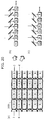
- FIG. 1 is a diagram showing an arrangement of photodiodes in a solid-state imaging device of a conventional technology.
- FIG. 2 is a diagram showing a cross section of the solid-state imaging device of the conventional technology.
- FIG. 3 is a diagram showing a color arrangement of photodiodes in a solid-state imaging device of a first embodiment.
- FIG. 4 is a diagram showing an arrangement of microlenses in the solid-state imaging device.
- FIG. 5 is a diagram showing a cross section of the solid-state imaging device.
- FIG. 6 is a pattern diagram showing cross sections of rows which are adjacent to each other.
- FIG. 7A is a cross-section diagram of a light-selecting unit for blue light.
- FIG. 7B is a cross-section diagram of a light-selecting unit for red light.
- FIG. 8A is a cross-section diagram of a light-reflecting unit 104 M.
- FIG. 8B is a cross-section diagram of a light-reflecting unit 104 M.
- FIG. 9A is a cross-section diagram of a light-selecting unit for blue light as a first variation of the light-selecting unit.
- FIG. 9B is a cross-section diagram of a light-selecting unit for red light as the first variation of the light-selecting unit.
- FIG. 10A is a cross-section diagram of a light-selecting unit for blue light as a second variation of the light-selecting unit.
- FIG. 10B is a cross-section diagram of a light-selecting unit for red light as the second variation of the light-selecting unit.
- FIG. 11 is a diagram showing a first variation of a color arrangement of photodiodes in the solid-state imaging device.
- FIG. 12 is a pattern diagram showing cross sections of rows which are adjacent to each other.
- FIG. 13 is a cross-section diagram of a solid-state imaging device of a second embodiment.
- FIG. 14A is a cross-section diagram of a light-selecting unit.
- FIG. 14B is a cross-section diagram of a light-selecting unit.
- FIG. 15A is a diagram showing the thicknesses of insulator layers and spectral characteristics of light-selecting units.
- FIGS. 15B and 15C are graphs showing transmission characteristics of a dielectric multilayer film which changes depending on whether or not the spacer layer is included in the film.
- FIG. 16 is a diagram showing a second variation of a color arrangement of photodiodes in the solid-state imaging device.
- FIG. 17 is a pattern diagram showing cross sections of rows which are adjacent to each other.
- FIG. 18 is a diagram showing a third variation of a color arrangement of photodiodes in the solid-state imaging device.
- FIG. 19 is a pattern diagram showing cross sections of rows which are adjacent to each other in the third variation.
- FIG. 20 is a pattern diagram showing cross sections of rows which are adjacent to each other in a fourth variation.
- FIG. 21 is a diagram showing a fifth variation of a color arrangement of photodiodes in the solid-state imaging device.
- FIG. 22 is a pattern diagram showing cross sections of rows which are adjacent to each other in the fifth variation.
- FIG. 23 is a diagram showing a sixth variation of a color arrangement of photodiodes in the solid-state imaging device.
- FIG. 24 is a pattern diagram showing cross sections of rows which are adjacent to each other in the sixth variation.
- FIG. 25 is a block diagram showing a structure of a camera in a third embodiment.
- FIG. 26 is an explanatory diagram of a color converting unit.
- a solid-state imaging device separates incident light entering through a microlens into first light having a wavelength within a predetermined range, and second light having a wavelength out of the predetermined range. Further, the first light enters a photodiode, and the second light enters a different photodiode. Further, for separating the incident light entering through the microlens, a multilayer film, having an insulator layer (also called a spacer layer) that has a photonic structure which is structured based on the wavelength within the predetermined range, is used. With this, sensitivity of the solid-state imaging device is enhanced.
- FIG. 3 is a top view showing a color arrangement of photodiodes in the solid-state imaging device of the first embodiment.
- the solid-state imaging device includes photodiodes which are two-dimensionally arranged.
- the above described first light enters one of two photodiodes which are adjacent to each other, and the above described second light enters the other photodiode.
- One of the types of pairs is a pair of a photodiode 102 B for receiving blue light and a photodiode 102 Ye for receiving yellow light, the color of which is a complementary color of blue.
- Another type of pairs is a pair of a photodiode 102 R for receiving red light and a photodiode 102 Cy for receiving cyan light, the color of which is a complementary color of red.
- the photodiodes include four types of photodiodes: a photodiode which corresponds to first primary color light indicating a first primary color, that is, one of the colors, red, green and blue; a photodiode which corresponds to first complementary color light indicating a first complementary color, that is, a complementary color of the first primary color; a photodiode which corresponds to second primary color light indicating a second primary color which is different from the first primary color; and a photodiode which corresponds to second complementary color light indicating a second primary color, that is, a complementary color of the second primary color.
- FIG. 4 is a top view showing an arrangement of microlenses in the solid-state imaging device.
- each of a plurality of microlenses 109 is provided to correspond to a pair of photodiodes, and serves as a light condenser which condenses light.
- the shape of each of the microlenses 109 is a rounded rhombic shape (a rounded square) as shown in the figure, the shape may be a circle or a square.
- the optical axis of each of the microlenses 109 is arranged in such way that it matches the center of a photodiode corresponding to a primary color, that is, a photodiode 102 B and 102 R.
- the microlenses 109 are arranged in such manner that the respective centers of the microlense 109 in a row are shifted from the respective centers of the microlenses 109 in a vertically adjacent row by a distance between the respective centers of two of the photodiodes which are horizontally adjacent.
- FIG. 5 is a diagram showing a cross section of the solid-state imaging device taken along the line A-A shown in FIG. 4 .
- the solid-state imaging device includes the photodiode 102 B and the photodiode 102 Ye which are positioned near a surface of a semiconductor substrate 101 .
- the photodiode 102 B and the photodiode 102 Ye are covered by a transparent film 103 which is made of a silica glass, for example.
- the transparent film 103 is formed in such manner that its top surface, opposite to its lower surface covering the photodiodes 102 B and 104 Ye, has a mountain range-like shape.
- a light-selecting unit 104 B and a light-reflecting unit 104 M are formed on inclined areas of the mountain range-like shaped top surface which are inclined by a fixed angle in the same direction.
- the light-selecting unit 104 B and the light-reflecting unit 104 M are positioned to correspond to the photodiode 102 B and the photodiode 102 Ye, respectively.
- the light-selecting unit 104 B has a characteristic that selectively: allows transmission of light which has a wavelength of blue light as the light having a wavelength within the predetermined range, among the incident light entering through the corresponding microlens 109 ; and reflects yellow light, the color of which is a complementary color of blue (that is, light having a wavelength which differs from the wavelength of blue light).
- the light-selecting unit 104 B is inclined so that the transmitted blue light enters the photodiode 102 B and that the reflected yellow light enters the light-reflecting unit 104 M which is positioned above the photodiode 102 Ye.
- the inclination angle of the light-selecting unit 104 B is preferred to be as close to 45° as possible so that the incident light from above is reflected towards the right direction of the figure, and is further reflected by the light-reflecting unit 104 M to enter the photodiode 102 Ye.
- the light-selecting unit 104 R has a characteristic that selectively: allows transmission of light which has a wavelength of red light, among the incident light entering through the corresponding microlens 109 ; and reflects cyan light, the color of which is a complementary color of red (that is, light having a wavelength which differs from the wavelength of red light).
- the light-selecting unit 104 R is inclined so that the transmitted red light enters the photodiode 102 R and that the reflected cyan light enters light-reflecting unit 104 M which is positioned above the photodiode 102 Cy.
- incident light which enters the light-selecting unit 104 B transmits or reflects off the light-selecting unit 104 B
- incident light which enters the light-selecting unit 104 R transmits or reflects off the light-selecting unit 104 R
- the wavelength range can be set selectively.
- a multilayer film called dichroic filter can be used, the dichroic filter being structured in the same manner as the filter formed on a surface of a dichroic prism in an electric still camera, a 3CCD video camera, and the like.
- a multilayer film including an insulator layer is used, the insulator layer having the photonic structure and being an improved version of the dichroic filter.
- the light-reflecting unit 104 M has a characteristic which reflects incident light, and includes a total reflection film which includes a metal film made of aluminum, for example.
- the light-selecting unit 104 B and the light-reflecting unit 104 M are covered by a transparent film 105 having a refractive index which is low compared to that of the transparent film 103 .
- the transparent film 105 On an area of the transparent film 105 that corresponds to the light-selecting unit 104 B, there is a concave lens 106 .
- the transparent film 105 is covered by a light-blocking film 107 .
- Through the aperture and the concave lens 106 light enters the light-selecting unit 104 B, and unnecessary light does not enter the light-selecting unit 104 R and the light-reflecting units 104 M which are adjacent to the light-selecting unit 104 B, since the unnecessary light is blocked by the light-blocking film 107 .
- the light-blocking film 107 and the concave lens 106 are covered by a transparent film 108 .
- the microlens 109 (a convex lens) is provided on an area of the transparent film 108 that corresponds to the photodiode 102 B. Accordingly, for each pair of one photodiode 102 B and one photodiode 102 Ye which are adjacent to each other, there is a light condenser made up of a pair of one microlens 109 and one concave lens 106 .
- Incident light is condensed by the microlens 109 and the concave lens 106 , and enters the light-selecting unit 104 B as collimated light.
- blue light B transmits the light-selecting unit 104 B and enters the blue photodiode 102 B.
- yellow light Ye the color of which is a complementary color of blue, is reflected by the light-selecting unit 104 B towards the light-reflecting unit 104 M which is positioned above the photodiode 102 Ye.
- Yellow light Ye reflects off the light-reflecting unit 104 M, and enters the photodiode 102 Ye.
- the light entering through the microlens 109 is separated into blue light and yellow light as the light-selecting unit 104 B and the light-reflecting unit 104 M reflect and/or allow transmission of the incident light. Further, blue light and yellow light are allocated to the corresponding photodiode 102 B or 102 Ye. Blue light enters the photodiode 102 B after transmitting the light-selecting unit 104 B once. Yellow light enters the photodiode 102 Ye after reflecting off twice of the light-selecting unit 104 B and the light-reflecting unit 104 M.
- the microlenses are arranged in 45° diagonal lines as shown in FIG. 4 , the distance between the respective centers of two of the microlenses which are vertically or horizontally adjacent to each other becomes 1.4 times longer than the distance between the respective centers of two of the photodiodes which are vertically or horizontally adjacent to each other. Further, the vertical resolution and the horizontal resolution can be controlled to be 1/1.4 of the number of the photodiodes.
- FIG. 6 is a pattern diagram showing directions of the light-selecting units and the light-reflecting units in rows adjacent to each other.
- a section (a) of the figure is a top view showing two rows which are adjacent to each other. In one of the rows, the blue photodiodes 102 B and the yellow photodiodes 102 Ye are alternately aligned. In the other row of the adjacent rows, the cyan photodiodes 102 Cy and the red photodiodes 102 R are alternately aligned.
- a section (b) of FIG. 6 is a pattern diagram showing a cross section taken along the line B-B.
- a reflecting surface of the light-selecting unit 104 B that selectively reflects yellow light having the wavelength different from the wavelength of blue light, faces the right direction of the figure, and a reflecting surface of the light-reflecting unit 104 M faces the left direction of the figure.
- the reflecting surface of the light-selecting unit 104 B and the reflecting surface of the light-reflecting unit 104 M face each other and both incline in the same direction (45° downward to the right in the figure).
- a section (c) of FIG. 6 is a pattern diagram showing a cross section taken along the line C-C.
- the light-reflecting unit 104 M and the light-selecting unit 104 R are aligned in the opposite manner to the one shown in the section (b). Therefore, a reflecting surface of the light-reflecting unit 104 M and a reflecting surface of the light-selecting unit 104 R face and incline in the opposite directions to the ones shown in the section (b).
- FIG. 7A and FIG. 7B are cross-section diagrams showing more detailed structures of the light-selecting unit 104 B and the light-selecting unit 104 R, respectively.
- the light-selecting unit 104 B is a multilayer film including a titanium dioxide layer 501 a, a silicon dioxide layer 501 b, a titanium dioxide layer 501 c, an insulator layer 501 B, a titanium dioxide layer 501 e , a silicon dioxide layer 501 f, and a titanium dioxide layer 501 g.
- the light-selecting unit 104 B is a dielectric multilayer film in which materials such as a silicon oxide layer (SiO 2 ) having a low refractive index and materials such as a titanium oxide layer (TiO 2 ) and a silicon nitride layer (Si 3 N 4 ) having a high refractive index are alternately layered, and in which the insulator layer 501 B is also included. All layers except for the insulator layer 501 B have the same optical thicknesses.
- optical thickness refers to a value nd which is a refractive index n of the material of the layer multiplied by the thickness d of the layer.
- the optical thicknesses of all layers 501 a to 501 g, except for the insulator layer 501 B, are a quarter of a wavelength ⁇ ( ⁇ /4) ( ⁇ is the wavelength of red light in FIGS. 7A and 7B ).
- the wavelength ⁇ which is set for each layer having the optical thickness of ⁇ /4 is called a set center wavelength.
- the light-selecting unit 104 R is different from the light-selecting unit 104 B in that the light-selecting unit 104 R includes a silicon dioxide layer 501 d having the optical thickness of ⁇ /4, instead of the insulator layer 501 B.
- the light-selecting unit 104 R does not include the insulator layer 501 B, and is structured in the same way as the dichroic filter in which each layer has the optical thickness of ⁇ /4. Therefore, the light-selecting unit 104 R selectively allows transmission of light having a wavelength which is equal to the set center wavelength ⁇ (red light in this case), and reflects light having a different wavelength.
- the light-selecting unit 104 R shown in FIG. 7B serves as a dichroic filter and a dichroic mirror which allow transmission of red light and reflect cyan light, the color of which is a complementary color of red. Note that transmission characteristics of the light-selecting unit 104 B and the light-selecting unit 104 R are shown in the lower part of FIG. 15A which is described later.
- the structure of the insulator layer 501 B shown in FIG. 7A has the photonic structure in which titanium dioxide and silicon dioxide are alternately aligned along the principal surface.
- the insulator layer 501 B has a characteristic which allows transmission of light having a wavelength other than ⁇ of the above ⁇ /4. That the light-selecting unit 104 B includes the insulator layer 501 B is one of the features of the present embodiment. More specifically, based on the optical thickness of the insulator layer 501 B, a wavelength range of light which transmits the light-selecting unit 104 B can be adjusted. In other words, by including the insulator layer 501 B, the light-selecting unit 104 B shown in FIG.
- the light-selecting unit 104 B is capable of selectively allowing transmission of light within a desired wavelength range (that is, blue light), and reflecting yellow light, the color of which is a complementary color of blue.
- the light-selecting unit 104 R may be a dichroic filter.
- the light-selecting unit 104 B includes the dielectric multilayer film which is included in the light-selecting unit 104 R, and the insulator layer inserted in the dielectric multilayer film. Based on the optical thickness of the insulator layer, the wavelength of light which transmits the light-selecting unit 104 B is adjusted to the wavelength of blue light.
- the light-selecting unit 104 B and the light-selecting unit 104 R both include the layers 501 a, 501 b, 501 c, 501 e, 501 f, and 501 g, and therefore, a commonality of manufacturing processes between the light-selecting unit 104 B and the light-selecting unit 104 R can be achieved, and the number of manufacturing man-hours can be reduced.
- the International Patent Publication WO 2005/069376 A1 discloses a technique of adjusting the transmission wavelength in such manner that the transmission wavelength is shifted from the set center wavelength, by providing an insulator layer in a dielectric multilayer film in which each layer has the optical thickness of ⁇ /4.
- the light-selecting units 104 B and 104 R can be manufactured based on this publication.
- FIGS. 8A and 8B are cross-section diagrams of the light-reflecting units 104 M.
- the light-reflecting unit 104 M shown in FIG. 8A includes an aluminium layer 601 a .
- the light-reflecting unit 104 M completely reflects the incident light entering from the light-selecting unit 104 B or the light-selecting unit 104 R towards the photodiode 102 Ye or the photodiode 102 Cy, respectively.
- the light-reflecting unit 104 M shown in FIG. 8B completely reflects visible light only, and serves as a removing unit which removes ultraviolet light and infrared light. Therefore, the light-reflecting unit 104 M shown in FIG. 8B is formed by a component such as a multilayer film having layers 601 b - 601 g which absorbs ultraviolet light and infrared light.
- the solid-state imaging device of the present invention is structured in such way that it separates incident light entering through the microlens 109 into the first primary color light having the wavelength within the predetermined range, and the first complementary color light having a wavelength out of the predetermined range.
- the first primary color light enters one of the photodiodes, and the first complementary color light enters another one of the photodiode.
- the light-selecting units 104 B and 104 R are used, the light-selecting units 104 B and 104 R including the multilayer film having the insulator layer that has the photonic structure which is structured based on the wavelength of the predetermined range. Accordingly, sensitivity of the solid-state imaging device can be enhanced, and a commonality of the manufacturing processes can be achieved, and thus the manufacturing cost can be reduced.
- FIG. 9A and FIG. 9B are diagrams showing cross-sections of the light-selecting unit 104 B and the light-selecting unit 104 R as a first variation of the light-selecting units 104 B and 104 R.
- the light-selecting unit 104 B shown in FIG. 9A is a dichroic filter structured by a multilayer film which includes a titanium dioxide layer 701 a , a silicon dioxide layer 701 b , a titanium dioxide layer 701 c , a silicon dioxide layer 701 d , a titanium dioxide layer 701 e , a silicon dioxide layer 701 f , and a titanium dioxide layer 701 g .
- the set center wavelength of the light-selecting unit 104 B is the wavelength of blue light.
- the light-selecting unit 104 R shown in FIG. 9B is different from the light-selecting unit 104 B shown in FIG. 9A in that there is an insulator layer 701 R having the photonic structure instead of the silicon dioxide layer 701 d . Based on the optical thickness of the insulator layer 701 R, the transmission wavelength of the light-selecting unit 104 R is adjusted to the wavelength of red light.
- the common layers 701 a , 701 b , 701 c , 701 e , 701 f and 701 g in the light-selecting unit 104 B and in the light-selecting unit 104 R share the same optical thicknesses, and thus these common layers can be manufactured at the same time for both types of the light-selecting units. Consequently, a commonality of the manufacturing processes is achieved, and thus the manufacturing cost can be reduced.
- FIG. 10A and FIG. 10B are diagrams showing cross-sections of the light-selecting unit 104 B and the light-selecting unit 104 R as a second variation of the light-selecting units 104 B and 104 R.
- the light-selecting unit 104 B shown in FIG. 10A is a multilayer film which includes a titanium dioxide layer 801 a , a silicon dioxide layer 801 b , a titanium dioxide layer 801 c , an insulator layer 801 B, a titanium dioxide layer 801 e , a silicon dioxide layer 801 f , and a titanium dioxide layer 801 g .
- the set center wavelength of all layers except for the insulator layer 801 B is, for example, the wavelength of green light rather than the wavelength of blue light or red light (the optical thickness of ⁇ /4, ⁇ being the wavelength of green light).
- the light-selecting unit 104 R shown in FIG. 10B is different from the light-selecting unit 104 B shown in FIG. 10A in that there is an insulator layer 801 R instead of the insulator layer 801 B.
- the insulator layer 801 B has the optical thickness which shifts the wavelength of light that transmits the light-selecting unit 104 B from the wavelength of green light to the wavelength of blue light, and the wavelength of light that transmits the light-selecting unit 104 B is adjusted to the wavelength of blue light.
- the insulator layer 801 R has the optical thickness which shifts the wavelength of light that transmits the light-selecting unit 104 R from the wavelength of green light to the wavelength of red light, and the wavelength of light that transmits the light-selecting unit 104 R is adjusted to the wavelength of red light.
- the common layers 801 a , 801 b , 801 c , 801 e , 801 f and 801 g in the light-selecting unit 104 B and in the light-selecting unit 104 R share the same optical thicknesses, and thus these common layers can be manufactured at the same time for both types of the light-selecting units. Consequently, a commonality of the manufacturing processes is achieved, and thus the manufacturing cost can be reduced.
- both the light-selecting unit 104 B and the light-selecting unit 104 R have an insulator layer. Therefore, the thickness of the light-selecting unit 104 B and the thickness of the light-selecting unit 104 R can be made equal to each other.
- pairs (B, Ye) and (R, Cy) are described as examples of pairs of a primary color and a complementary color, any two arbitrary pairs may be selected from among the pairs (B, Ye), (R, Cy) and (G, Mg).
- FIG. 11 is a diagram showing a first variation of a color arrangement of the photodiodes in pairs of a primary color and a complementary color.
- photodiodes 102 G and photodiodes 102 Mg which correspond to (G, Mg), respectively, are alternately arranged.
- the photodiodes 102 Cy and the photodiodes 102 R which correspond to (Cy, R), respectively, are alternately arranged.
- FIG. 12 is a pattern diagram showing an arrangement of the microlenses 109 and cross sections of the rows adjacent to each other in FIG. 11 .
- the microlenses 109 are arranged in such manner that the center of each of the microlenses 109 matches the center of a photodiode which corresponds to a primary color, that is, the photodiode 102 G and 102 R.
- the light-selecting units 104 and the light-reflecting units 104 M in one of any two rows adjacent to each other incline in the opposite direction to the direction in which the light-selecting units 104 and the light-reflecting units 104 M in the other row of the adjacent rows incline.
- the color arrangement shown in FIG. 11 is the most preferable color arrangement. This is because in FIG. 15A , a width at a half value of blue light is narrower that that of green light and of red light.
- the sensitivity of the solid-state imaging device can be further enhanced.
- the present embodiment describes an example of adjusting the optical thickness based on the physical thickness, instead of adjusting the optical thickness based on an insulator layer having the photonic structure in the light-selecting units 104 .
- FIG. 13 is a cross-section diagram of a solid-state imaging device of the second embodiment.
- the arrangement of photodiodes shown in FIG. 13 is assumed to be the arrangement shown in FIG. 11 in which the rows of (G, Mg) and the rows of (Cy, R) are alternately arranged.
- the cross-section diagram shown in FIG. 13 is different from the cross-section diagram shown in FIG. 5 in that the cross-section diagram of FIG. 13 includes the photodiode 102 Mg and the photodiode 102 G instead of the photodiode 102 Ye and the photodiode 102 B, and includes a light-selecting unit 904 G instead of the light-selecting unit 104 B.
- the cross-section diagram of FIG. 13 includes the photodiode 102 Mg and the photodiode 102 G instead of the photodiode 102 Ye and the photodiode 102 B, and includes a light-selecting unit 904 G instead of the light-selecting unit 104 B.
- the photodiode 102 Mg and the photodiode 102 G have the same structures as the photodiode 102 Ye and the photodiode 102 B in a physical sense, however there is a difference in light which enters.
- the light-selecting unit 904 G is different from the light-selecting unit 104 B in that the insulator layer does not have the photonic structure.
- FIG. 14A and FIG. 14B are cross-section diagrams showing more detailed structures of the light-selecting unit 904 R and the light-selecting unit 904 G, respectively.
- the light-selecting unit 904 R is a multilayer film including a titanium dioxide layer 201 a , a silicon dioxide layer 201 b , a titanium dioxide layer 201 c , an insulator layer 201 R, a titanium dioxide layer 201 e , a silicon dioxide layer 201 f , and a titanium dioxide layer 201 g . All layers except for the insulator layer 201 R have the same optical thicknesses.
- All layers 201 a to 201 g except for the insulator layer 201 R have the set center wavelength which is the wavelength of green light.
- the insulator layer 201 R shown in FIG. 14A is made of silicon dioxide, and has the optical thickness different from ⁇ /4, ⁇ being the wavelength of green light. Based on the optical thickness of the insulator layer 201 R, a wavelength range of light which transmits the light-selecting unit 904 R can be adjusted. In other words, by including the insulator layer 201 R, the light-selecting unit 904 R shown in FIG. 14A shifts the transmission wavelength of the dichroic filter in which each layer has the optical thickness of ⁇ /4, ⁇ being the wavelength of green light.
- the light-selecting unit 904 R is capable of selectively allowing transmission of light within a desired wavelength range (that is, red light), and reflecting cyan light, the color of which is a complementary color of red.
- the light-selecting unit 904 G shown in FIG. 14B is different from the light-selecting unit 104 B in that the light-selecting unit 904 G includes a silicon dioxide layer 201 d which has the optical thickness of ⁇ /4. Since the light-selecting unit 904 G does not include the insulator layer 201 R, it means that the light-selecting unit 904 G has the same structure as the dichroic filter in which each layer has the optical thickness of ⁇ /4, provided that the wavelength of green light is set as the set center wavelength. Therefore, the light-selecting unit 904 G allows transmission of light which has the wavelength equal to the set center wavelength ⁇ (green light in this case). Accordingly, the light-selecting unit 904 G shown in FIG. 14B serves as a dichroic filter and a dichroic mirror which allow transmission of green light, and which reflect magenta light, the color of which is a complementary color of green.
- FIG. 15A is a diagram showing spectral characteristics of the light-selecting units 904 B, 904 G and 904 R.
- the light-selecting unit 904 G shown in the figure is the light-selecting unit 904 G shown in FIG. 14B .
- the thickness of the insulator layer (spacer layer) is 0 nm.
- the light-selecting unit 904 B shown in FIG. 15A has a structure in which an insulator layer (spacer layer) having the thickness of 200 nm is added to the multilayer film of the light-selecting unit 904 G shown in FIG. 14B .
- the light-selecting unit 904 R shown in FIG. 15A has a structure in which an insulator layer (spacer layer) having the thickness of 50 nm is added to the multilayer film of the light-selecting unit 904 G shown in FIG. 14B .
- the spectral characteristics of the light-selecting units 904 B, 904 G and 904 R are derived using a characteristic matrix method. Further, the spectral characteristics are derived with an assumption that the refractive index of titanium dioxide (material having a high refractive index) is 2.5, the refractive index of silicon dioxide (material having a low refractive index) is 1.45, and the optical thickness and physical thickness of the insulator layer (spacer layer) are 200 nm and 80 nm for the light-selecting unit 904 B, 50 nm and 20 nm for the light-selecting unit 904 R, and 0 nm for the light-selecting unit 904 G.
- titanium dioxide such material as silicon nitride, tantalum pentoxide, and zirconium dioxide may be used as the material having a high refractive index. Further, a material other than silicon dioxide may be used as the material having a low refractive index.
- FIGS. 15B and 15C are graphs showing a transmission characteristic of a dielectric multilayer film which changes depending on whether or not a spacer layer is included in the film. Note that the transmission characteristics shown in FIGS. 15B and 15C are derived using a matrix method in which a Fresnel coefficient is used, and are the transmission characteristics of vertical incident light only which are derived with an assumption that the pair number is 10 and the set center wavelength is 550 nm. The vertical axis of each of the graphs indicates transmittance, and the horizontal axis indicates a wavelength of incident light which enters the dielectric multilayer film.
- the entire dielectric multilayer film which includes silicon nitride and silicon dioxide is a multilayer film having the optical thickness of ⁇ /4
- light having the wavelength within a wavelength range is reflected as FIG. 15B shows, the wavelength range having the set center wavelength as the center of the range.
- the larger the difference is between the refractive index of a multilayer film material having a high refractive index and the refractive index of a multilayer film material having a low refractive index the larger the reflection bandwidth expands.
- the dielectric multilayer film is formed in such manner that multilayer films having the optical thickness of ⁇ /4 are provided to sandwich the spacer layer having the optical thickness other than ⁇ /4 and are symmetric to each other with respect to the spacer layer, it is possible to obtain the light-selecting units 904 which allow transmission of only light that has the wavelength near the set center wavelength in the reflection band of the multilayer film which has the optical thickness of ⁇ /4, as shown in FIG. 15C .
- the thicknesses of the light-selecting units 904 can be approximately the wavelength of incident light (approximately 500 nm). Therefore, it is possible to minitualize the solid-state imaging device.
- FIGS. 15A to 15C also apply to the insulator layer having the photonic structure in the first embodiment. This is because in the case where the insulator layer having the photonic structure is used, instead of adjusting the physical thickness, the refractive index is adjusted based on a pitch and an arrangement of the photonic structure, which results in an adjustment of the optical thickness.
- the light-selecting unit 904 R and the light-selecting unit 904 G both include the common layers 201 a , 201 b , 201 c , 201 e , 201 f and 201 g . Therefore, a commonality of manufacturing processes between the light-selecting unit 904 R and the light-selecting unit 904 G can be achieved, and the number of manufacturing man-hours can be reduced.
- the International Patent Publication WO 2005/069376 A1 discloses the technique of adjusting the transmission wavelength in such manner that the transmission wavelength is shifted from the set center wavelength, by providing an insulator layer in a dielectric multilayer film in which each layer has the optical thickness of ⁇ /4 and by adjusting the optical thickness of the provided insulator layer.
- the light-selecting units 904 R and 904 G can be manufactured based on this publication.
- FIG. 16 is a diagram showing a second variation of a color arrangement of the photodiodes which are in pairs of a primary color and a complementary color.
- the photodiodes 102 B and the photodiodes 102 Ye, as the pairs (B, Ye) are alternately arranged.
- the photodiodes 102 R and the photodiodes 102 Cy are alternately arranged.
- the position of the pair of the photodiodes in one of any two rows which are adjacent to each other is shifted from the position of the pair of the photodiodes in the other row of the adjacent rows by one photodiode (by one pixel).
- a photodiode 102 X which is at the head of each (R, Cy) row (shown as X in the figure) is not used.
- FIG. 17 is a pattern diagram, corresponding to FIG. 16 , showing an arrangement of the microlenses 109 , and cross sections of rows adjacent to each other.
- the shape of each of the microlenses 109 is a rounded rhombic shape (square).
- the microlenses 109 are arranged in such manner that the center of each of the microlenses 109 matches the center of a photodiode which corresponds to a primary color, that is, the photodiode 102 B and 102 R. As shown in FIG.
- shifting the position of the pair of the photodiodes in one of any two rows adjacent to each other from the position of the pair of photodiodes in the other row of the adjacent rows by one pixel (by one photodiode) allows both the light-selecting units 104 and the light-reflecting units 104 M in any two rows adjacent to each other to incline in the same direction, as shown in sections (b) and (c) of FIG. 17 . Therefore, it is possible to enhance manufacturing reliability.
- FIG. 18 is a diagram showing a third variation of the color arrangement of the photodiodes in the solid-state imaging device.
- the photodiode which corresponds to a primary color and the photodiode which corresponds to another primary color are positioned in the same columns.
- the photodiodes 102 Ye and the photodiodes 102 B, as the pairs (Ye, B) are alternately arranged.
- the photodiodes 102 Cy and the photodiodes 102 R as the pairs (Cy, R), are alternately arranged.
- FIG. 19 is a pattern diagram, corresponding to FIG. 18 , showing an arrangement of the microlenses 109 , and cross-sections of rows adjacent to each other. As shown in a section (a) of FIG. 19 , the shape of each of the microlenses 109 is almost a rectangular. The microlenses 109 are arranged in such manner that the center of each of the microlenses 109 matches the center of a photodiode which corresponds to a primary color, that is, a photodiode 102 B and 102 R. As shown in FIG.
- the photodiodes which, among the photodiodes in pairs, correspond to primary colors in the same columns allows both the light-selecting units 104 and the light-reflecting units 104 M in any two rows adjacent to each other to incline in the same direction as shown in sections (b) and (c) of FIG. 19 . Therefore, it becomes easy to uniform inclination degrees of all light-selecting units 104 and all light-reflecting units 104 M.
- the arrangement of the microlenses 109 shown in FIG. 19 enables an increase in the resolution in a specific direction with respect to incident light. More specifically, with the solid-state imaging device of the present embodiment, the vertical arrangement pitch and the horizontal arrangement pitch of the microlenses 109 differ from each other. The vertical arrangement pitch is 1 ⁇ 2 of the horizontal arrangement pitch. As a result, this structure allows the vertical resolution to be twice the horizontal resolution.
- FIG. 20 is a pattern diagram showing a fourth variation of an arrangement of the microlenses 109 and cross-sections of rows adjacent to each other. This figure corresponds to the color arrangement of the photodiodes shown in FIG. 18 , however, as shown in sections (b) and (c) of FIG. 20 , the position of the pair of the photodiodes in one of any two rows adjacent to each other is shifted from the position of the pair of the photodiodes in the other row of the adjacent rows by one photodiode. In other words, the photodiodes 102 X are not used.
- the light-selecting unit 104 and the light-reflecting unit 104 M in one of any two rows adjacent to each other incline in the opposite direction to the direction in which the light-selecting unit 104 and the light-reflecting unit 104 M in the other row of the adjacent rows incline.
- FIG. 21 is a diagram showing a fifth variation of a color arrangement of the photodiodes in pairs of a primary color and a complementary color.
- two types of pairs that is the pairs (B, Ye) and the pairs (Cy, R) are alternately aligned in each row. In any two rows adjacent to each other, different pairs are vertically adjacent to each other.
- FIG. 22 is a pattern diagram, corresponding to FIG. 21 , showing an arrangement of the microlenses 109 and cross-sections of rows adjacent to each other.
- the center of each of the microlenses 109 does not match the center of the photodiode 102 which corresponds to a primary color nor the center of the photodiode 102 which corresponds to a complementary color.
- the microlenses 109 need to be formed in such manner that each of the microlenses 109 condenses incident light in a direction towards the photodiode 102 which corresponds to a primary color or the photodiode 102 which corresponds to another primary color.
- the light-selecting unit 104 and light-reflecting unit 104 M in one of any two rows adjacent to each other incline in the opposite direction to the direction in which the light-selecting unit 104 and the light-reflecting unit 104 M in the other row of the adjacent rows incline.
- FIG. 23 is a diagram showing a sixth variation of a color arrangement of the photodiodes in pairs of a primary color and a complementary color.
- pairs (R, Cy) are aligned, and in the other column of the adjacent columns, pairs (Ye, B) are aligned.
- FIG. 24 is a pattern diagram, corresponding to FIG. 23 , showing an arrangement of the microlenses 109 , and cross-sections of rows adjacent to each other. As shown in a section (a) of FIG. 24 , the center of each of the microlenses 109 matches the center of the photodiode 102 which correspond to a primary color.
- a section (b) of FIG. 24 is a pattern diagram showing a vertical cross section taken along the line O-O.
- a section (c) of FIG. 24 is a pattern diagram showing a vertical cross section taken along the line P-P. As shown in the figure, each pair may be a pair of two photodiodes which are vertically adjacent to each other.
- the microlenses 109 are also rearranged in such way that the long sides of the rectangles are vertically aligned. As a result, this arrangement allows the horizontal resolution to be twice the vertical resolution.
- the light-selecting unit 104 selectively allows transmission of primary color light and reflects complementary color light.
- the light-selecting unit 104 may selectively allow transmission of the complementary color light and reflect the primary color light.
- the microlenses 109 may be arranged in such manner that the center of each of the microlenses 109 matches the center of the photodiode 102 which corresponds to a complementary color.
- microlenses 109 may be arranged in such manner that each of the microlenses 109 in one of any two rows adjacent to each other matches the photodiode 102 which corresponds to a primary color, and the center of each of the microlenses 109 in the other row of the adjacent rows matches the photodiode 102 which corresponds to a complementary color.
- the present embodiment describes signal processing for converting color signals which are obtained by the solid-state imaging device of each of the above described embodiments into signals of three primary colors.
- FIG. 25 is a block diagram showing configuration of a camera according to the third embodiment.
- a camera 401 of the present embodiment includes a signal processing unit 410 , a solid-state imaging device 411 , a driving unit 412 , a controlling unit 414 , a mechanical shutter 415 , a lens 416 and a displaying unit 420 .
- the signal processing unit 410 includes a color converting unit 413 , and performs color conversion by obtaining signals of each of the photodiodes outputted by the solid-state imaging device 411 .
- the solid-state imaging device 411 is the solid-state imaging device of the above described first and second embodiments. Light from an imaging subject enters the solid-state imaging device via the lens 416 and the mechanical shutter 415 . As an imaging result, the solid-state imaging device 411 outputs, in sequence, signals respectively indicating the first primary color, the first complementary color, the second primary color, and the second complementary color obtained from four photodiodes to the signal processing unit 410 .
- a pair of the first primary color signal and the first complementary color signal represents one of the following pairs: (B signal, Ye signal), (R signal, Cy signal) and (G signal, Mg signal).
- a pair of the second primary color signal and the second complementary color signal represents one of the other pairs mentioned above.
- the driving unit 412 outputs various driving signals for driving the solid-state imaging device 411 .
- the controlling unit 414 controls the entire camera 401 .
- the displaying unit 420 makes a display on a monitor and a display of a captured image.
- FIG. 26 is an explanatory diagram of the color converting unit 413 .
- the color converting unit 413 converts the first primary color signal, the first complementary color signal, the second primary color signal and the second complementary color signal into a red signal, a green signal, and a blue signal. This color conversion can be performed using a well-known operation.
- a filter may be provided to serve as a removing unit which removes ultraviolet light and infrared light.
- the solid-state imaging device may be a Charge Coupled Device (CCD) type solid-state imaging device or a Metal Oxide Semiconductor (MOS) type solid-state imaging device.
- CCD Charge Coupled Device
- MOS Metal Oxide Semiconductor
- a material having a high refractive index such material as silicon nitride, tantalum pentoxide, and zirconium dioxide may be used instead of using the above described titanium dioxide.
- a material having a low refractive index a material other than silicon dioxide may be used.
- the number of layers in the multilayer film of the light-selecting units is not limited to the number shown in the above described embodiments, and may be any number. It is needless to say that a material of each layer is not limited to the above mentioned titanium dioxide, silicon dioxide, and magnesium oxide. Instead, tantalum oxide (Ta 2 O 5 ), zirconium oxide (ZrO 2 ), silicon nitride (SiN), silicon nitride (Si 3 N 5 ), aluminium oxide (Al 2 O 3 ), magnesium fluoride (MgF 2 ) and hafnium oxide (HfO 3 ) may be used.
- the present invention is applicable to a solid-state imaging device having photodiodes which are formed on a semiconductor substrate, and to a camera having such a solid-state imaging device.
- the present invention is applicable to a CCD image sensor, a MOS image sensor, a digital still camera, a camera equipped mobile phone, a monitoring camera, a camera built in a laptop computer, a camera unit connected to an information processing apparatus and the like.
Landscapes
- Physics & Mathematics (AREA)
- Spectroscopy & Molecular Physics (AREA)
- Engineering & Computer Science (AREA)
- Multimedia (AREA)
- Signal Processing (AREA)
- Color Television Image Signal Generators (AREA)
- Solid State Image Pick-Up Elements (AREA)
- Blocking Light For Cameras (AREA)
- Transforming Light Signals Into Electric Signals (AREA)
Abstract
Description
Claims (17)
Applications Claiming Priority (2)
| Application Number | Priority Date | Filing Date | Title |
|---|---|---|---|
| JP2006-108035 | 2006-04-10 | ||
| JP2006108035A JP4740018B2 (en) | 2006-04-10 | 2006-04-10 | Solid-state imaging device, camera, and signal processing method |
Publications (2)
| Publication Number | Publication Date |
|---|---|
| US20070235756A1 US20070235756A1 (en) | 2007-10-11 |
| US7863633B2 true US7863633B2 (en) | 2011-01-04 |
Family
ID=38140447
Family Applications (1)
| Application Number | Title | Priority Date | Filing Date |
|---|---|---|---|
| US11/697,498 Active 2028-12-31 US7863633B2 (en) | 2006-04-10 | 2007-04-06 | Solid-state imaging device, camera and signal processing method |
Country Status (6)
| Country | Link |
|---|---|
| US (1) | US7863633B2 (en) |
| EP (1) | EP1845559A1 (en) |
| JP (1) | JP4740018B2 (en) |
| KR (1) | KR20070101139A (en) |
| CN (1) | CN101056365A (en) |
| TW (1) | TW200810101A (en) |
Cited By (3)
| Publication number | Priority date | Publication date | Assignee | Title |
|---|---|---|---|---|
| US20110007179A1 (en) * | 2009-01-14 | 2011-01-13 | Masao Hiramoto | Image capture device |
| US9159756B2 (en) * | 2014-01-21 | 2015-10-13 | Kabushiki Kaisha Toshiba | Solid-state imaging device and manufacturing method of the same |
| US10834343B2 (en) | 2016-11-08 | 2020-11-10 | Samsung Electronics Co., Ltd. | Image sensor including color splitting element and method of operating the image sensor |
Families Citing this family (22)
| Publication number | Priority date | Publication date | Assignee | Title |
|---|---|---|---|---|
| JP2008060726A (en) * | 2006-08-29 | 2008-03-13 | Matsushita Electric Ind Co Ltd | Solid-state imaging device |
| JP4688766B2 (en) * | 2006-09-21 | 2011-05-25 | パナソニック株式会社 | Solid-state imaging device, driving method thereof and camera |
| US7701024B2 (en) * | 2006-12-13 | 2010-04-20 | Panasonic Corporation | Solid-state imaging device, manufactoring method thereof and camera |
| US8085331B2 (en) * | 2007-12-21 | 2011-12-27 | Panasonic Corporation | Solid-state imaging device, driving method thereof, and camera |
| KR100907892B1 (en) * | 2007-12-24 | 2009-07-15 | 주식회사 동부하이텍 | Image sensor and its manufacturing method |
| JP5055643B2 (en) * | 2008-07-28 | 2012-10-24 | 株式会社リコー | Image pickup device and image pickup apparatus |
| JP5113249B2 (en) * | 2008-11-19 | 2013-01-09 | パナソニック株式会社 | Imaging device |
| WO2010070869A1 (en) * | 2008-12-19 | 2010-06-24 | パナソニック株式会社 | Image pickup device |
| KR20110121531A (en) * | 2009-03-05 | 2011-11-07 | 파나소닉 주식회사 | Solid-State Imaging Device and Imaging Device |
| JP5121764B2 (en) | 2009-03-24 | 2013-01-16 | 株式会社東芝 | Solid-state imaging device |
| KR101625209B1 (en) * | 2009-12-11 | 2016-05-30 | 삼성전자주식회사 | Color filter array based on dichroic filter |
| JP5337212B2 (en) * | 2011-09-02 | 2013-11-06 | 株式会社東芝 | Solid-state image sensor |
| CN103222267B (en) * | 2011-10-31 | 2017-02-08 | 松下电器(美国)知识产权公司 | Solid-state imaging element, imaging device, and signal processing method |
| JP5774502B2 (en) * | 2012-01-12 | 2015-09-09 | 株式会社東芝 | Solid-state imaging device |
| US9099370B2 (en) | 2012-09-03 | 2015-08-04 | Panasonic Intellectual Property Management Co., Ltd. | Solid-state imaging element and imaging device |
| JP6368993B2 (en) * | 2013-07-24 | 2018-08-08 | 株式会社ニコン | Imaging device |
| KR101463963B1 (en) * | 2013-09-17 | 2014-11-27 | (주)실리콘화일 | Image Sensor Chip |
| KR102163727B1 (en) * | 2014-04-03 | 2020-10-08 | 삼성전자주식회사 | Image sensor having improved light utilization efficiency |
| JP2016096163A (en) * | 2014-11-12 | 2016-05-26 | ソニー株式会社 | Solid-state image sensor, manufacturing method and electronic apparatus |
| WO2019159561A1 (en) * | 2018-02-13 | 2019-08-22 | ソニーセミコンダクタソリューションズ株式会社 | Solid-state imaging element, electronic device, and method for manufacturing solid-state imaging element |
| CN114447006A (en) | 2020-10-30 | 2022-05-06 | 三星电子株式会社 | Image sensor including color separation lens array and electronic device including image sensor |
| JP7016557B1 (en) | 2021-01-14 | 2022-02-07 | 株式会社タナカ技研 | Imaging device |
Citations (4)
| Publication number | Priority date | Publication date | Assignee | Title |
|---|---|---|---|---|
| JP2000151933A (en) | 1998-11-06 | 2000-05-30 | Nec Corp | Image pickup element and its manufacture |
| US20030063204A1 (en) | 2001-08-31 | 2003-04-03 | Canon Kabushiki Kaisha | Image pickup apparatus |
| EP1341235A2 (en) | 2002-02-28 | 2003-09-03 | Canon Kabushiki Kaisha | Image pickup apparatus |
| WO2005069376A1 (en) * | 2004-01-15 | 2005-07-28 | Matsushita Electric Industrial Co.,Ltd. | Solid state imaging device, process for fabricating solid state imaging device and camera employing same |
Family Cites Families (3)
| Publication number | Priority date | Publication date | Assignee | Title |
|---|---|---|---|---|
| JPH09205589A (en) * | 1996-01-26 | 1997-08-05 | Sony Corp | Solid-state imaging device |
| JP2005142429A (en) * | 2003-11-07 | 2005-06-02 | Matsushita Electric Ind Co Ltd | Solid-state imaging device and manufacturing method thereof |
| JP4836625B2 (en) * | 2006-03-24 | 2011-12-14 | パナソニック株式会社 | Solid-state image sensor |
-
2006
- 2006-04-10 JP JP2006108035A patent/JP4740018B2/en not_active Expired - Fee Related
-
2007
- 2007-03-27 TW TW096110520A patent/TW200810101A/en unknown
- 2007-04-05 EP EP07105773A patent/EP1845559A1/en not_active Withdrawn
- 2007-04-06 US US11/697,498 patent/US7863633B2/en active Active
- 2007-04-09 KR KR1020070034687A patent/KR20070101139A/en not_active Withdrawn
- 2007-04-10 CN CNA2007100960538A patent/CN101056365A/en active Pending
Patent Citations (6)
| Publication number | Priority date | Publication date | Assignee | Title |
|---|---|---|---|---|
| JP2000151933A (en) | 1998-11-06 | 2000-05-30 | Nec Corp | Image pickup element and its manufacture |
| US20030063204A1 (en) | 2001-08-31 | 2003-04-03 | Canon Kabushiki Kaisha | Image pickup apparatus |
| EP1341235A2 (en) | 2002-02-28 | 2003-09-03 | Canon Kabushiki Kaisha | Image pickup apparatus |
| US20040004668A1 (en) | 2002-02-28 | 2004-01-08 | Canon Kabushiki Kaisha | Image pickup apparatus |
| WO2005069376A1 (en) * | 2004-01-15 | 2005-07-28 | Matsushita Electric Industrial Co.,Ltd. | Solid state imaging device, process for fabricating solid state imaging device and camera employing same |
| US20060205107A1 (en) * | 2004-01-15 | 2006-09-14 | Yuuichi Inaba | Solid-state imaging device, manufacturing method of solid-state imaging device, and camera employing same |
Non-Patent Citations (2)
| Title |
|---|
| English Language Abstract of JP 2000-151933. |
| U.S. Appl. No. 11/621,276 to Kato, filed Jan. 9, 2007. |
Cited By (4)
| Publication number | Priority date | Publication date | Assignee | Title |
|---|---|---|---|---|
| US20110007179A1 (en) * | 2009-01-14 | 2011-01-13 | Masao Hiramoto | Image capture device |
| US8289422B2 (en) * | 2009-01-14 | 2012-10-16 | Panasonic Corporation | Image capture device |
| US9159756B2 (en) * | 2014-01-21 | 2015-10-13 | Kabushiki Kaisha Toshiba | Solid-state imaging device and manufacturing method of the same |
| US10834343B2 (en) | 2016-11-08 | 2020-11-10 | Samsung Electronics Co., Ltd. | Image sensor including color splitting element and method of operating the image sensor |
Also Published As
| Publication number | Publication date |
|---|---|
| TW200810101A (en) | 2008-02-16 |
| US20070235756A1 (en) | 2007-10-11 |
| JP4740018B2 (en) | 2011-08-03 |
| EP1845559A1 (en) | 2007-10-17 |
| KR20070101139A (en) | 2007-10-16 |
| JP2007282054A (en) | 2007-10-25 |
| CN101056365A (en) | 2007-10-17 |
Similar Documents
| Publication | Publication Date | Title |
|---|---|---|
| US7863633B2 (en) | Solid-state imaging device, camera and signal processing method | |
| US7538363B2 (en) | Solid-state imaging device and method for fabricating the same | |
| KR100508068B1 (en) | Image pickup apparatus | |
| US8134191B2 (en) | Solid-state imaging device, signal processing method, and camera | |
| KR100553056B1 (en) | Image pickup apparatus | |
| JP4806197B2 (en) | Solid-state imaging device | |
| US7759679B2 (en) | Solid-state imaging device, manufacturing method of solid-state imaging device, and camera employing same | |
| US7550709B2 (en) | Solid-state imaging device and method for fabricating the same | |
| US10393576B2 (en) | Image sensor including color filter isolation layer and method of manufacturing the same | |
| US10187595B2 (en) | Solid-state image sensor | |
| JP2003078917A (en) | Imaging device | |
| JP2012074521A (en) | Manufacturing method of solid-state image pickup device, solid-state image pickup device, and electronic equipment | |
| JP2000151933A (en) | Image pickup element and its manufacture | |
| JP2006190958A (en) | Physical information acquisition method and physical information acquisition device | |
| US10276612B2 (en) | Photoelectric conversion apparatus and image pickup system | |
| JP2007220832A (en) | Solid-state imaging device and camera | |
| JP4887915B2 (en) | Solid-state imaging device | |
| US9159756B2 (en) | Solid-state imaging device and manufacturing method of the same | |
| JP4298209B2 (en) | Imaging apparatus and system | |
| JP2008060323A (en) | Solid-state imaging device, method for manufacturing solid-state imaging device, and camera | |
| JP2004193284A (en) | Imaging device | |
| JP2012156194A (en) | Solid state imaging device and imaging apparatus | |
| JP2009194572A (en) | Solid-state imaging device and camera | |
| JP2008067058A (en) | Solid-state imaging device, signal processing method, and camera | |
| JP2008153308A (en) | Solid-state image sensing device and camera |
Legal Events
| Date | Code | Title | Description |
|---|---|---|---|
| AS | Assignment |
Owner name: MATSUSHITA ELECTRIC INDUSTRIAL CO., LTD., JAPAN Free format text: ASSIGNMENT OF ASSIGNORS INTEREST;ASSIGNOR:KATO, YOSHIAKI;REEL/FRAME:019888/0506 Effective date: 20070326 |
|
| AS | Assignment |
Owner name: PANASONIC CORPORATION, JAPAN Free format text: CHANGE OF NAME;ASSIGNOR:MATSUSHITA ELECTRIC INDUSTRIAL CO., LTD.;REEL/FRAME:021897/0534 Effective date: 20081001 Owner name: PANASONIC CORPORATION,JAPAN Free format text: CHANGE OF NAME;ASSIGNOR:MATSUSHITA ELECTRIC INDUSTRIAL CO., LTD.;REEL/FRAME:021897/0534 Effective date: 20081001 |
|
| FEPP | Fee payment procedure |
Free format text: PAYOR NUMBER ASSIGNED (ORIGINAL EVENT CODE: ASPN); ENTITY STATUS OF PATENT OWNER: LARGE ENTITY |
|
| STCF | Information on status: patent grant |
Free format text: PATENTED CASE |
|
| FPAY | Fee payment |
Year of fee payment: 4 |
|
| AS | Assignment |
Owner name: PANNOVA SEMIC, LLC, CALIFORNIA Free format text: ASSIGNMENT OF ASSIGNORS INTEREST;ASSIGNOR:PANASONIC CORPORATION;REEL/FRAME:036065/0273 Effective date: 20141226 |
|
| FEPP | Fee payment procedure |
Free format text: PAYER NUMBER DE-ASSIGNED (ORIGINAL EVENT CODE: RMPN); ENTITY STATUS OF PATENT OWNER: LARGE ENTITY Free format text: PAYOR NUMBER ASSIGNED (ORIGINAL EVENT CODE: ASPN); ENTITY STATUS OF PATENT OWNER: LARGE ENTITY |
|
| MAFP | Maintenance fee payment |
Free format text: PAYMENT OF MAINTENANCE FEE, 8TH YEAR, LARGE ENTITY (ORIGINAL EVENT CODE: M1552) Year of fee payment: 8 |
|
| MAFP | Maintenance fee payment |
Free format text: PAYMENT OF MAINTENANCE FEE, 12TH YEAR, LARGE ENTITY (ORIGINAL EVENT CODE: M1553); ENTITY STATUS OF PATENT OWNER: LARGE ENTITY Year of fee payment: 12 |