US7855108B2 - Semiconductor heterojunction devices based on SiC - Google Patents

Semiconductor heterojunction devices based on SiC Download PDF

Info

Publication number
US7855108B2
US7855108B2 US12/713,753 US71375310A US7855108B2 US 7855108 B2 US7855108 B2 US 7855108B2 US 71375310 A US71375310 A US 71375310A US 7855108 B2 US7855108 B2 US 7855108B2
Authority
US
United States
Prior art keywords
sic
epitaxial film
growing
film
grown
Prior art date
Legal status (The legal status is an assumption and is not a legal conclusion. Google has not performed a legal analysis and makes no representation as to the accuracy of the status listed.)
Active
Application number
US12/713,753
Other versions
US20100192840A1 (en
Inventor
Narsingh B. Singh
Brian P. Wagner
David J. Knuteson
Michael E. Aumer
Andre Berghmans
Darren Thomson
David Kahler
Current Assignee (The listed assignees may be inaccurate. Google has not performed a legal analysis and makes no representation or warranty as to the accuracy of the list.)
Northrop Grumman Systems Corp
Original Assignee
Northrop Grumman Systems Corp
Priority date (The priority date is an assumption and is not a legal conclusion. Google has not performed a legal analysis and makes no representation as to the accuracy of the date listed.)
Filing date
Publication date
Application filed by Northrop Grumman Systems Corp filed Critical Northrop Grumman Systems Corp
Priority to US12/713,753 priority Critical patent/US7855108B2/en
Publication of US20100192840A1 publication Critical patent/US20100192840A1/en
Application granted granted Critical
Publication of US7855108B2 publication Critical patent/US7855108B2/en
Assigned to NORTHROP GRUMMAN SYSTEMS CORPORATION reassignment NORTHROP GRUMMAN SYSTEMS CORPORATION ASSIGNMENT OF ASSIGNORS INTEREST (SEE DOCUMENT FOR DETAILS). Assignors: NORTHROP GRUMMAN CORPORATION
Active legal-status Critical Current
Anticipated expiration legal-status Critical

Links

Images

Classifications

    • HELECTRICITY
    • H10SEMICONDUCTOR DEVICES; ELECTRIC SOLID-STATE DEVICES NOT OTHERWISE PROVIDED FOR
    • H10DINORGANIC ELECTRIC SEMICONDUCTOR DEVICES
    • H10D30/00Field-effect transistors [FET]
    • H10D30/01Manufacture or treatment
    • H10D30/015Manufacture or treatment of FETs having heterojunction interface channels or heterojunction gate electrodes, e.g. HEMT
    • HELECTRICITY
    • H10SEMICONDUCTOR DEVICES; ELECTRIC SOLID-STATE DEVICES NOT OTHERWISE PROVIDED FOR
    • H10DINORGANIC ELECTRIC SEMICONDUCTOR DEVICES
    • H10D10/00Bipolar junction transistors [BJT]
    • H10D10/01Manufacture or treatment
    • H10D10/021Manufacture or treatment of heterojunction BJTs [HBT]
    • HELECTRICITY
    • H10SEMICONDUCTOR DEVICES; ELECTRIC SOLID-STATE DEVICES NOT OTHERWISE PROVIDED FOR
    • H10DINORGANIC ELECTRIC SEMICONDUCTOR DEVICES
    • H10D10/00Bipolar junction transistors [BJT]
    • H10D10/80Heterojunction BJTs
    • HELECTRICITY
    • H10SEMICONDUCTOR DEVICES; ELECTRIC SOLID-STATE DEVICES NOT OTHERWISE PROVIDED FOR
    • H10DINORGANIC ELECTRIC SEMICONDUCTOR DEVICES
    • H10D12/00Bipolar devices controlled by the field effect, e.g. insulated-gate bipolar transistors [IGBT]
    • H10D12/01Manufacture or treatment
    • H10D12/031Manufacture or treatment of IGBTs
    • HELECTRICITY
    • H10SEMICONDUCTOR DEVICES; ELECTRIC SOLID-STATE DEVICES NOT OTHERWISE PROVIDED FOR
    • H10DINORGANIC ELECTRIC SEMICONDUCTOR DEVICES
    • H10D30/00Field-effect transistors [FET]
    • H10D30/40FETs having zero-dimensional [0D], one-dimensional [1D] or two-dimensional [2D] charge carrier gas channels
    • H10D30/47FETs having zero-dimensional [0D], one-dimensional [1D] or two-dimensional [2D] charge carrier gas channels having 2D charge carrier gas channels, e.g. nanoribbon FETs or high electron mobility transistors [HEMT]
    • H10D30/471High electron mobility transistors [HEMT] or high hole mobility transistors [HHMT]
    • H10D30/472High electron mobility transistors [HEMT] or high hole mobility transistors [HHMT] having lower bandgap active layer formed on top of wider bandgap layer, e.g. inverted HEMT
    • HELECTRICITY
    • H10SEMICONDUCTOR DEVICES; ELECTRIC SOLID-STATE DEVICES NOT OTHERWISE PROVIDED FOR
    • H10DINORGANIC ELECTRIC SEMICONDUCTOR DEVICES
    • H10D30/00Field-effect transistors [FET]
    • H10D30/40FETs having zero-dimensional [0D], one-dimensional [1D] or two-dimensional [2D] charge carrier gas channels
    • H10D30/47FETs having zero-dimensional [0D], one-dimensional [1D] or two-dimensional [2D] charge carrier gas channels having 2D charge carrier gas channels, e.g. nanoribbon FETs or high electron mobility transistors [HEMT]
    • H10D30/471High electron mobility transistors [HEMT] or high hole mobility transistors [HHMT]
    • H10D30/475High electron mobility transistors [HEMT] or high hole mobility transistors [HHMT] having wider bandgap layer formed on top of lower bandgap active layer, e.g. undoped barrier HEMTs such as i-AlGaN/GaN HEMTs
    • HELECTRICITY
    • H10SEMICONDUCTOR DEVICES; ELECTRIC SOLID-STATE DEVICES NOT OTHERWISE PROVIDED FOR
    • H10DINORGANIC ELECTRIC SEMICONDUCTOR DEVICES
    • H10D62/00Semiconductor bodies, or regions thereof, of devices having potential barriers
    • H10D62/80Semiconductor bodies, or regions thereof, of devices having potential barriers characterised by the materials
    • H10D62/83Semiconductor bodies, or regions thereof, of devices having potential barriers characterised by the materials being Group IV materials, e.g. B-doped Si or undoped Ge
    • H10D62/832Semiconductor bodies, or regions thereof, of devices having potential barriers characterised by the materials being Group IV materials, e.g. B-doped Si or undoped Ge being Group IV materials comprising two or more elements, e.g. SiGe
    • H10D62/8325Silicon carbide

Definitions

  • a semiconductor device has a doped silicon carbide heterojunction.
  • Gallium nitride is a typical wide-bandgap semiconductor material that has potential applications in high-speed, high power transistor devices.
  • One of the main drawbacks to the production of these devices is the limited availability of suitable substrates for epitaxial growth.
  • a high-quality bulk single crystal substrate such as silicon carbide (SiC), having low cost and having a large area, is desirable for the growth of GaN and other types of epitaxial layers for device fabrication.
  • the GaN epitaxial layer is homoepitaxially grown on a single crystal GaN substrate.
  • the cost and availability of these wafers are prohibitive.
  • GaN devices gallium arsenide (GaAs) metal-semiconductor field effect transistors (MESFETs) were the dominant devices for high frequency applications.
  • GaAs gallium arsenide
  • MESFETs metal-semiconductor field effect transistors
  • HEMTs High electron mobility transistors
  • the optimized MESFETs show a maximum operating frequency (f max ) of 160 GHz, while GaAs pseudomorphic high electron mobility transistors (PHEMTs) have attained maximum frequency (fmax) values of 290 GHz, and InP PHEMTs have attained frequencies of 600 GHz.
  • f max maximum operating frequency
  • PHEMTs GaAs pseudomorphic high electron mobility transistors
  • fmax maximum frequency
  • InP PHEMTs have attained frequencies of 600 GHz.
  • GaN films are produced by hetereoepitaxial growth on either single crystal SiC or sapphire. Due to the lattice mismatch between GaN (4.8 ⁇ ) and sapphire (4.763 ⁇ ) or 4H-silicon carbide (3.0730 ⁇ ), a significant number of threading dislocations are formed during the growth process.
  • SiC has become an important wide bandgap group III-V semiconductor because of its excellent properties for high power microwave devices. SiC thus competes with GaAs and Si in terms of gain, power output and efficiency at X-band, and promises even better performance at higher frequencies (Ka and Ku-bands).
  • a particular goal for this technology is efficient broadband power RF transmitters that have high efficiency and high linearity, as well as rugged and low noise receivers for transmit/receive (T/R) modules for microwave applications.
  • one aspect of the present invention is directed at producing a substrate that substantially obviates one or more problems due to limitations and disadvantages of the related art.
  • An aspect of the invention is to provide an Al doped SiC substrate grown using a physical vapor transport (PVT) method.
  • PVT physical vapor transport
  • One aspect of the technology pertains to a semiconductor device that includes SiC layer over which is grown a metal-doped epitaxial layer.
  • Another aspect of the invention pertains to a method for forming a semiconductor device on a SiC substrate by growing an epitaxial film of Si (1-x) M x C over the substrate, wherein M is Al, Ge or In and x is 0 to 1.
  • FIG. 1 shows the advantages of the invention that can be attained over the related art technology.
  • FIGS. 2 a - 2 d show HEMT structures using (Si 1-x M x )C containing heterostructures.
  • FIG. 3 is a scanning electron microscope (SEM) photomicrograph of cleaving damage in a heterostructure.
  • FIG. 4 is an SEM photomicrograph of a heterostructure cross section.
  • FIG. 5 shows the morphology of Si (1-x) Al x C grown using PVD (Area A).
  • FIG. 6 shows another view of the morphology of Si (1-x) Al x C grown using PVD.
  • FIG. 7 shows the energy dispersive spectrometry (EDS) spectrum of Si (1-x) Al x C grown using PVD.
  • FIG. 8 shows the auger electron spectrometry (AES) spectrum of Si (1-x) Al x C grown using PVD.
  • Utilizing Al as a dopant significantly affects the mobility and other properties of SiC materials and heterostructures that can be formed from SiC. This ability to form SiC/AlSiC permits the manufacture of higher performance SiC devices.
  • HEMTs high electron mobility transistors
  • HBTs heterojunction bipolar transistors
  • group III-V material systems these materials provide performance far superior to MSFETs and bipolar junction transistors (BJTs), and have been important in increasing the high frequency performance of power devices.
  • the invention provides a route to form similar devices utilizing SiC systems. Improvements can be attained in SiC MESFETs through the introduction of an SiC/Si (1-x) M x C heterostructure, where M is Al, Ge or In.
  • the invention provides energy band offsets with the possibility of attaining wider offsets. These values are similar or superior to those found in conventional art III-V materials.
  • FIG. 1 shows the advantages of the invention when used to form two-dimensional electron gas (2DEG) heterostructures when compared to the related art technology, where Ev is the valence band energy, Ef is the Fermi band energy and Ec is the conduction and energy.
  • Ev is the valence band energy
  • Ef is the Fermi band energy
  • Ec is the conduction and energy.
  • FIG. 1 shows that the related art technology such as AlGaN/GaN is prone to defect formation that can lead to gate lag (surface trapping), drain lag (buffer trapping), radio frequency (RF) dispersion, high gate leakage and even current collapse.
  • the inventive doping of Al, In or Ge into the SiC substrate can reduce defect structures to alleviate these problems.
  • the related art AlGaN/GaN technology can produce an electron mobility of 1300 cm 2 Nsec at 300° K, but the Al, In or Ge doped hetero structure of the invention may attain an electron mobility in the range of about 1500-1800 cm 2 Nsec at 300° K.
  • the Al, In or Ge doped heterostructure of the invention may attain very high radiation tolerance and breakdown voltage.
  • the related art AlGaN/GaN technology can have an operating voltage equivalent to a GaN device
  • the Al, In or Ge doped heterostructure of the invention may attain an operating voltage of about twice that of a GaN device.
  • the HEMT issues mentioned above lead to uncertain reliability for the related art AlGaN/GaN technology, but the doping technology of the invention yields SiC devices having high reliability.
  • FIGS. 2 a - 2 d show the HEMT structures that can be attained using the (Si 1-x M x )C containing heterostructures of the invention.
  • FIG. 2 a shows an SiC substrate 2 over which is formed an SiC 4 buffer layer, an (Si 1-x M x )C channel 6 , an SiC barrier layer 8 and an n+SiC layer 10 .
  • M can be Al, Ge or In.
  • the 2DEG layer can be found at the interface of the (Si 1-x Al x )C channel 6 and the SiC barrier layer 8 .
  • FIG. 1 shows an SiC substrate 2 over which is formed an SiC 4 buffer layer, an (Si 1-x M x )C channel 6 , an SiC barrier layer 8 and an n+SiC layer 10 .
  • M can be Al, Ge or In.
  • the 2DEG layer can be found at the interface of the (Si 1-x Al x )C channel 6 and the SiC barrier layer 8 .
  • 2 b shows an SiC substrate 12 over which is formed an SiC buffer layer 14 , an SiC channel layer 16 , an (Si 1-x M x )C barrier layer 18 , and an N+ (Si 1-x Ge x )C layer 20 .
  • M can be Al, Ge or In.
  • the 2DEG layer can be found at the interface of the SiC channel layer 16 and the (Si 1-x M x )C barrier layer 17 .
  • FIGS. 2 c and 2 d show transistor structures respectively formed on the SiC heterostructures of FIGS. 2 a and 2 b .
  • an optional active layer 22 may be formed in FIGS. 2 b and 2 c .
  • a source 24 , a gate 26 and a drain 28 may be formed in FIGS. 2 b and 2 c .
  • a passivation layer 30 may be formed in FIGS. 2 c and 2 d may be formed from SiC materials.
  • the transistor structures may be formed using Si, GaN or AlGaN technologies in the conventional manner.
  • the transistors thus formed may be high frequency mobility transistors (HFMTs), heterojunction bipolar transistors (HBTs), or high electron mobility transistors (HEMTs).
  • HFMTs high frequency mobility transistors
  • HBTs heterojunction bipolar transistors
  • HEMTs high electron mobility transistors
  • the structures shown in FIGS. 2 a - 2 d may be formed using epitaxial growth methods such as vapor deposition, molecular beam epitaxy or sputtering. Other methods for forming the structures may also be used, including chemical vapor deposition (CVD). Appropriate CVD methods may include atmospheric pressure CVD (APCVD), sub-atmospheric pressure CVD (SACVD), low pressure CVD (LPCVD), plasma enhanced CVD (PECVD), high-density plasma CVD (HDPCVD), metal organic CVD (MOCVD) and vapor phase epitaxy (VPE). Semiconductor bonding techniques may also be used.
  • APCVD atmospheric pressure CVD
  • SACVD sub-atmospheric pressure CVD
  • LPCVD low pressure CVD
  • PECVD plasma enhanced CVD
  • HDPCVD high-density plasma CVD
  • MOCVD metal organic CVD
  • VPE vapor phase epitaxy
  • Semiconductor bonding techniques may also be used
  • the substrate may be a 6H SiC wafer with (001) orientation.
  • the source SiC material may be powder.
  • Aluminum (Al) can be used as the dopant, but other dopants may be used, including germanium (Ge) or indium (In). Aluminum may preferably be used as the dopant.
  • Approximately 0-10%, preferably 0.01-10%, more preferably 5-7% and most preferably 6% of dopant may be placed in a crucible in a growth chamber.
  • Argon may be preferably used in the growth chamber, however, any suitable inert gas or gas mixture may be used.
  • a growth run of up to about 30 hours may produce an epitaxially grown film. The growth time depends on the desired thickness of the film, and a run time of about 15 hours may produce a film thickness of about 12 ⁇ m.
  • the source temperature may be in the range of about 1800 to 2200° C.
  • the chamber pressure may range from about 50 to 400 Torr.
  • the substrate was an existing 6H SiC wafer with (001) orientation.
  • the source SiC material was powder.
  • Aluminum was used as the dopant. Approximately 6% aluminum was placed in the crucible. Argon was used in the growth chamber. A growth run of 15 hours produced epitaxially grown film. The growth conditions are shown in Table 1.
  • FIG. 3 shows the cross-sectional morphology of the as-grown film.
  • SEM scanning electron microscope
  • FIG. 4 shows another SEM view of the cross section of the as-grown film.
  • the smoothness of the surface of the film can be readily observed.
  • FIG. 5 shows an SEM view of the surface of the Al film deposited on a SiC substrate in accordance with the invention.
  • the large smooth areas indicate the low defect density of the formed Al film.
  • the low defect density typically shown in FIG. 5 allows the formation of structures having minimal lattice defects over the film surface.
  • FIG. 6 is another SEM view of the surface of the Al film deposited on a SiC substrate in accordance with the invention.
  • FIG. 6 shows the even morphology of the surface structure and the lack of significant pitting or line defects.
  • the smooth surface structures shown in FIGS. 5 and 6 allow an optimal junction formation to obtain a two dimensional electron gas (2-DEG)
  • FIG. 7 The results for energy dispersive spectrometry (EDS) are shown in FIG. 7 .
  • the peak for Al is readily observed in the neighborhood of 1400 eV.
  • FIG. 8 verifies the composition to be about 6% Al, 27% Si and 66% C.
  • the film quality was also evaluated using an X-ray method.
  • the lattice parameter was observed to be very close to pure SiC.
  • the invention provides an Si (1-x) M x C material for heterostructures on SiC that can be grown by CVD, PVD or MOCVD.
  • SiC preferably doped with Al, modifies the bandgap and hence the hetero structure.
  • the growth of SiC—Si (1-x) M x C heterojunctions using SiC and Al sources permits the fabrication of improved high frequency mobility transistors (HFMTs), heterojunction bipolar transistors (HBTs), and high electron mobility transistors (HEMTs).
  • HFMTs high frequency mobility transistors
  • HBTs heterojunction bipolar transistors
  • HEMTs high electron mobility transistors

Landscapes

  • Junction Field-Effect Transistors (AREA)
  • Bipolar Transistors (AREA)

Abstract

A Si(1-x)MxC material for heterostructures on SiC can be grown by CVD, PVD and MOCVD. SIC doped with a metal such as Al modifies the bandgap and hence the heterostructure. Growth of SiC Si(1-x)MxC heterojunctions using SiC and metal sources permits the fabrication of improved HFMTs (high frequency mobility transistors), HBTs (heterojunction bipolar transistors), and HEMTs (high electron mobility transistors).

Description

BACKGROUND OF THE INVENTION
1. Field of the Invention
A semiconductor device has a doped silicon carbide heterojunction.
2. Description of the Related Art
Gallium nitride (GaN) is a typical wide-bandgap semiconductor material that has potential applications in high-speed, high power transistor devices. One of the main drawbacks to the production of these devices is the limited availability of suitable substrates for epitaxial growth. A high-quality bulk single crystal substrate such as silicon carbide (SiC), having low cost and having a large area, is desirable for the growth of GaN and other types of epitaxial layers for device fabrication. In one example of a related art technology, the GaN epitaxial layer is homoepitaxially grown on a single crystal GaN substrate. However, the cost and availability of these wafers are prohibitive.
Conventional heterostructures have already attained improved performance for high frequency group III-V semiconductor devices such as GaN devices. Initially, gallium arsenide (GaAs) metal-semiconductor field effect transistors (MESFETs) were the dominant devices for high frequency applications. Subsequently, several different heterostructures were developed in this material system, including AlGaAs/GaAs, (ΔEg ˜0.4 eV) and InAlAs/InGaAs (ΔEg ˜0.8 eV). High electron mobility transistors (HEMTs) utilizing these heterostructures can outperform their MESFET counterparts. For example, the optimized MESFETs show a maximum operating frequency (fmax) of 160 GHz, while GaAs pseudomorphic high electron mobility transistors (PHEMTs) have attained maximum frequency (fmax) values of 290 GHz, and InP PHEMTs have attained frequencies of 600 GHz.
Currently, GaN films are produced by hetereoepitaxial growth on either single crystal SiC or sapphire. Due to the lattice mismatch between GaN (4.8 Å) and sapphire (4.763 Å) or 4H-silicon carbide (3.0730 Å), a significant number of threading dislocations are formed during the growth process.
In the search to achieve large diameter, low defect, high quality SiC structures at affordable prices, SiC has become an important wide bandgap group III-V semiconductor because of its excellent properties for high power microwave devices. SiC thus competes with GaAs and Si in terms of gain, power output and efficiency at X-band, and promises even better performance at higher frequencies (Ka and Ku-bands). A particular goal for this technology is efficient broadband power RF transmitters that have high efficiency and high linearity, as well as rugged and low noise receivers for transmit/receive (T/R) modules for microwave applications.
As the technology advances, silicon carbide has become a good candidate. However, no heterostructure device has been achieved due to the unavailability of suitable SiC heterostructure material.
There is thus a need for practical metal-doped SiC materials that fulfill the requirements for wide bandgap semiconductor devices.
SUMMARY OF THE INVENTION
Accordingly, one aspect of the present invention is directed at producing a substrate that substantially obviates one or more problems due to limitations and disadvantages of the related art.
An aspect of the invention is to provide an Al doped SiC substrate grown using a physical vapor transport (PVT) method.
One aspect of the technology pertains to a semiconductor device that includes SiC layer over which is grown a metal-doped epitaxial layer.
Another aspect of the invention pertains to a method for forming a semiconductor device on a SiC substrate by growing an epitaxial film of Si(1-x)MxC over the substrate, wherein M is Al, Ge or In and x is 0 to 1.
It is to be understood that both the foregoing general description and the following detailed description of the invention are exemplary and explanatory and are intended to provide further explanation of the invention as claimed.
BRIEF DESCRIPTION OF THE DRAWINGS
The accompanying drawings, which are included to provide a further understanding of the invention and are incorporated in and constitute a part of this application, illustrate embodiments of the invention and together with the description serve to explain the principle of the invention.
In the drawings:
FIG. 1 shows the advantages of the invention that can be attained over the related art technology.
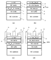
FIGS. 2 a-2 d show HEMT structures using (Si1-xMx)C containing heterostructures.
FIG. 3 is a scanning electron microscope (SEM) photomicrograph of cleaving damage in a heterostructure.
FIG. 4 is an SEM photomicrograph of a heterostructure cross section.
FIG. 5 shows the morphology of Si(1-x)AlxC grown using PVD (Area A).
FIG. 6 shows another view of the morphology of Si(1-x)AlxC grown using PVD.
FIG. 7 shows the energy dispersive spectrometry (EDS) spectrum of Si(1-x)AlxC grown using PVD.
FIG. 8 shows the auger electron spectrometry (AES) spectrum of Si(1-x)AlxC grown using PVD.
DETAILED DESCRIPTION
Reference will now be made in detail to the preferred embodiments of the invention, examples of which are illustrated in the accompanying drawings.
Utilizing Al as a dopant significantly affects the mobility and other properties of SiC materials and heterostructures that can be formed from SiC. This ability to form SiC/AlSiC permits the manufacture of higher performance SiC devices.
By adjusting the energy band gap by doping, for example with Al, devices such as high electron mobility transistors (HEMTs) and heterojunction bipolar transistors (HBTs) can be formed. In group III-V material systems, these materials provide performance far superior to MSFETs and bipolar junction transistors (BJTs), and have been important in increasing the high frequency performance of power devices. The invention provides a route to form similar devices utilizing SiC systems. Improvements can be attained in SiC MESFETs through the introduction of an SiC/Si(1-x)MxC heterostructure, where M is Al, Ge or In. The invention provides energy band offsets with the possibility of attaining wider offsets. These values are similar or superior to those found in conventional art III-V materials.
FIG. 1 shows the advantages of the invention when used to form two-dimensional electron gas (2DEG) heterostructures when compared to the related art technology, where Ev is the valence band energy, Ef is the Fermi band energy and Ec is the conduction and energy. When a wide band gap material is doped and placed adjacent to a narrow band gap material, the carrier starts to move from their parent dopants in the wide band gap material to the narrow band gap material due to the availability of states at lower energy. At the boundary, the band gap discontinuity causes the conduction band of the narrow band gap material to dip below the Fermi level. This band bending, which is a result due to charge transfer, and dipping of energy below the Fermi level causes the electron concentration to be very high at that point. This region of high electron concentration is so thin that it is described as a two-dimensional electron gas (2-DEG).
FIG. 1 shows that the related art technology such as AlGaN/GaN is prone to defect formation that can lead to gate lag (surface trapping), drain lag (buffer trapping), radio frequency (RF) dispersion, high gate leakage and even current collapse. In contrast, the inventive doping of Al, In or Ge into the SiC substrate can reduce defect structures to alleviate these problems. For example, the related art AlGaN/GaN technology can produce an electron mobility of 1300 cm2Nsec at 300° K, but the Al, In or Ge doped hetero structure of the invention may attain an electron mobility in the range of about 1500-1800 cm2Nsec at 300° K. Although the related art AlGaN/GaN technology can yield high radiation tolerance and high breakdown voltage, the Al, In or Ge doped heterostructure of the invention may attain very high radiation tolerance and breakdown voltage. Although the related art AlGaN/GaN technology can have an operating voltage equivalent to a GaN device, the Al, In or Ge doped heterostructure of the invention may attain an operating voltage of about twice that of a GaN device. Further, the HEMT issues mentioned above lead to uncertain reliability for the related art AlGaN/GaN technology, but the doping technology of the invention yields SiC devices having high reliability.
FIGS. 2 a-2 d show the HEMT structures that can be attained using the (Si1-xMx)C containing heterostructures of the invention. FIG. 2 a shows an SiC substrate 2 over which is formed an SiC 4 buffer layer, an (Si1-xMx)C channel 6, an SiC barrier layer 8 and an n+SiC layer 10. In the (Si1-xMx)C channel 6, M can be Al, Ge or In. In FIG. 2 a the 2DEG layer can be found at the interface of the (Si1-xAlx)C channel 6 and the SiC barrier layer 8. FIG. 2 b shows an SiC substrate 12 over which is formed an SiC buffer layer 14, an SiC channel layer 16, an (Si1-xMx)C barrier layer 18, and an N+ (Si1-xGex)C layer 20. In the (Si1-xMx)C barrier layer 18, M can be Al, Ge or In. In FIG. 2 b the 2DEG layer can be found at the interface of the SiC channel layer 16 and the (Si1-xMx)C barrier layer 17.
After the heterostructures shown in FIGS. 2 a and 2 b are formed, a power device such as a transistor can be manufactured. FIGS. 2 c and 2 d show transistor structures respectively formed on the SiC heterostructures of FIGS. 2 a and 2 b. In FIGS. 2 b and 2 c, an optional active layer 22 may be formed. Then, a source 24, a gate 26 and a drain 28 may be formed. Also, a passivation layer 30 may be formed. The transistors of FIGS. 2 c and 2 d may be formed from SiC materials. Alternately, the transistor structures may be formed using Si, GaN or AlGaN technologies in the conventional manner. The transistors thus formed may be high frequency mobility transistors (HFMTs), heterojunction bipolar transistors (HBTs), or high electron mobility transistors (HEMTs).
The structures shown in FIGS. 2 a-2 d may be formed using epitaxial growth methods such as vapor deposition, molecular beam epitaxy or sputtering. Other methods for forming the structures may also be used, including chemical vapor deposition (CVD). Appropriate CVD methods may include atmospheric pressure CVD (APCVD), sub-atmospheric pressure CVD (SACVD), low pressure CVD (LPCVD), plasma enhanced CVD (PECVD), high-density plasma CVD (HDPCVD), metal organic CVD (MOCVD) and vapor phase epitaxy (VPE). Semiconductor bonding techniques may also be used.
In the invention, the substrate may be a 6H SiC wafer with (001) orientation. The source SiC material may be powder. Aluminum (Al) can be used as the dopant, but other dopants may be used, including germanium (Ge) or indium (In). Aluminum may preferably be used as the dopant.
Approximately 0-10%, preferably 0.01-10%, more preferably 5-7% and most preferably 6% of dopant (such as Ge, In or preferably Al) may be placed in a crucible in a growth chamber. Argon may be preferably used in the growth chamber, however, any suitable inert gas or gas mixture may be used. A growth run of up to about 30 hours may produce an epitaxially grown film. The growth time depends on the desired thickness of the film, and a run time of about 15 hours may produce a film thickness of about 12 μm. The source temperature may be in the range of about 1800 to 2200° C. The chamber pressure may range from about 50 to 400 Torr.
Example 1
The substrate was an existing 6H SiC wafer with (001) orientation. The source SiC material was powder. Aluminum was used as the dopant. Approximately 6% aluminum was placed in the crucible. Argon was used in the growth chamber. A growth run of 15 hours produced epitaxially grown film. The growth conditions are shown in Table 1.
TABLE 1
Growth Conditions For Al-doped SiC Film.
Parameter Values
Growth Method PVT technique
Seed orientation On-axis 6H-SiC (0001)
Source Temp. 1800° C.
Seed Temp. 1745° C.
Pressure in 400 Torr Argon
Chamber
Growth time 15 hours
Source material 94% (by weight) SiC powder
6% High purity Al pieces
Composition Si(1−x)AlxC film with approximately 6% Al, x =
0.06
Film thickness 12 μm
Cracks No cracks observed
The film was characterized using a scanning electron microscope (SEM) for the morphology of the as-grown film. FIG. 3 shows the cross-sectional morphology of the as-grown film. In FIG. 3, the formation of the film over the substrate can readily observed. Some cleavage damage is an artifact of the preparation of the cross-sectional sample for SEM observation.
FIG. 4 shows another SEM view of the cross section of the as-grown film. In FIG. 4, the smoothness of the surface of the film can be readily observed.
FIG. 5 shows an SEM view of the surface of the Al film deposited on a SiC substrate in accordance with the invention. The large smooth areas indicate the low defect density of the formed Al film. The low defect density typically shown in FIG. 5 allows the formation of structures having minimal lattice defects over the film surface. FIG. 6 is another SEM view of the surface of the Al film deposited on a SiC substrate in accordance with the invention. FIG. 6 shows the even morphology of the surface structure and the lack of significant pitting or line defects. The smooth surface structures shown in FIGS. 5 and 6 allow an optimal junction formation to obtain a two dimensional electron gas (2-DEG)
The results for energy dispersive spectrometry (EDS) are shown in FIG. 7. The peak for Al is readily observed in the neighborhood of 1400 eV. The integration of auger electron spectroscopy (AES) peaks is shown in FIG. 8. FIG. 8 verifies the composition to be about 6% Al, 27% Si and 66% C.
The film quality was also evaluated using an X-ray method. For the 6% Al doping concentration, the lattice parameter was observed to be very close to pure SiC.
Accordingly, the invention provides an Si(1-x)MxC material for heterostructures on SiC that can be grown by CVD, PVD or MOCVD. SiC, preferably doped with Al, modifies the bandgap and hence the hetero structure. The growth of SiC—Si(1-x)MxC heterojunctions using SiC and Al sources permits the fabrication of improved high frequency mobility transistors (HFMTs), heterojunction bipolar transistors (HBTs), and high electron mobility transistors (HEMTs).
It is to be understood that the foregoing descriptions and specific embodiments shown herein are merely illustrative of the best mode of the invention and the principles thereof, and that modifications and additions may be easily made by those skilled in the art without departing for the spirit and scope of the invention, which is therefore understood to be limited only by the scope of the appended claims.

Claims (8)

1. A method for manufacturing a semiconductor device, comprising:
providing an SiC substrate; and
growing an epitaxial film of Si(1-x)MxC to form a heterojunction over the substrate, wherein M is Al or In and x is greater than 0 and less than 1, and wherein the heterojunction comprises a Si(1-x )MxC or SiC channel layer, a SiC or Si(1-x)MxC barrier, respectively, on top of the channel layer, and a n+SiC layer or n+Si(1-x)GexC, respectively, on top of the barrier layer.
2. The method of claim 1, wherein M is Al and x is 0.06.
3. The method of claim 1, wherein in the step of growing the epitaxial film, a source temperature is about 1800 to 2200° C.
4. The method of claim 1, wherein the step of growing the epitaxial film, a seed temperature is about 1700-2100° C.
5. The method of claim 1, wherein in the step of growing the epitaxial film, a seed temperature is about 1745° C.
6. The method of claim 1, wherein in the step of growing the epitaxial film, the epitaxial film is grown under a pressure of about 50 to 400 Torr argon.
7. The method of claim 1, wherein in the step of growing the epitaxial film, the epitaxial film is grown for about 15 hours.
8. The method of claim 1, wherein the epitaxial film comprises doped SiC.
US12/713,753 2006-06-26 2010-02-26 Semiconductor heterojunction devices based on SiC Active US7855108B2 (en)

Priority Applications (1)

Application Number Priority Date Filing Date Title
US12/713,753 US7855108B2 (en) 2006-06-26 2010-02-26 Semiconductor heterojunction devices based on SiC

Applications Claiming Priority (2)

Application Number Priority Date Filing Date Title
US11/474,398 US7683400B1 (en) 2006-06-26 2006-06-26 Semiconductor heterojunction devices based on SiC
US12/713,753 US7855108B2 (en) 2006-06-26 2010-02-26 Semiconductor heterojunction devices based on SiC

Related Parent Applications (1)

Application Number Title Priority Date Filing Date
US11/474,398 Division US7683400B1 (en) 2006-06-26 2006-06-26 Semiconductor heterojunction devices based on SiC

Publications (2)

Publication Number Publication Date
US20100192840A1 US20100192840A1 (en) 2010-08-05
US7855108B2 true US7855108B2 (en) 2010-12-21

Family

ID=38657593

Family Applications (2)

Application Number Title Priority Date Filing Date
US11/474,398 Active US7683400B1 (en) 2006-06-26 2006-06-26 Semiconductor heterojunction devices based on SiC
US12/713,753 Active US7855108B2 (en) 2006-06-26 2010-02-26 Semiconductor heterojunction devices based on SiC

Family Applications Before (1)

Application Number Title Priority Date Filing Date
US11/474,398 Active US7683400B1 (en) 2006-06-26 2006-06-26 Semiconductor heterojunction devices based on SiC

Country Status (4)

Country Link
US (2) US7683400B1 (en)
EP (1) EP2041795B1 (en)
JP (1) JP5286259B2 (en)
WO (1) WO2008002521A2 (en)

Cited By (1)

* Cited by examiner, † Cited by third party
Publication number Priority date Publication date Assignee Title
CN102881718A (en) * 2011-07-12 2013-01-16 三星电子株式会社 Nitride-based semiconductor device having excellent stability

Families Citing this family (1)

* Cited by examiner, † Cited by third party
Publication number Priority date Publication date Assignee Title
DE112023005782T5 (en) * 2023-02-14 2025-11-27 Mitsubishi Electric Corporation Semiconductor device and method for manufacturing a semiconductor device

Citations (1)

* Cited by examiner, † Cited by third party
Publication number Priority date Publication date Assignee Title
US20040256613A1 (en) * 2003-06-18 2004-12-23 Katsuya Oda Semiconductor device, semiconductor circuit module and manufacturing method of the same

Family Cites Families (7)

* Cited by examiner, † Cited by third party
Publication number Priority date Publication date Assignee Title
US5281831A (en) 1990-10-31 1994-01-25 Kabushiki Kaisha Toshiba Optical semiconductor device
SE9503630D0 (en) 1995-10-18 1995-10-18 Abb Research Ltd A semiconductor device having a heterojunction
JP3201993B2 (en) * 1998-04-28 2001-08-27 松下電器産業株式会社 Semiconductor device and manufacturing method thereof
US6221700B1 (en) 1998-07-31 2001-04-24 Denso Corporation Method of manufacturing silicon carbide semiconductor device with high activation rate of impurities
SE9900358D0 (en) 1999-02-03 1999-02-03 Ind Mikroelektronikcentrum Ab A lateral field effect transistor of SiC, a method of production thereof and a use of such a transistor
DE60042045D1 (en) 1999-06-22 2009-06-04 Panasonic Corp Heterojunction bipolar transistors and corresponding manufacturing methods
JP4874527B2 (en) * 2004-04-01 2012-02-15 トヨタ自動車株式会社 Silicon carbide semiconductor substrate and method for manufacturing the same

Patent Citations (1)

* Cited by examiner, † Cited by third party
Publication number Priority date Publication date Assignee Title
US20040256613A1 (en) * 2003-06-18 2004-12-23 Katsuya Oda Semiconductor device, semiconductor circuit module and manufacturing method of the same

Cited By (2)

* Cited by examiner, † Cited by third party
Publication number Priority date Publication date Assignee Title
CN102881718A (en) * 2011-07-12 2013-01-16 三星电子株式会社 Nitride-based semiconductor device having excellent stability
US20130015463A1 (en) * 2011-07-12 2013-01-17 Samsung Electronics Co., Ltd. Nitride-based semiconductor device having excellent stability

Also Published As

Publication number Publication date
US7683400B1 (en) 2010-03-23
JP2009542032A (en) 2009-11-26
WO2008002521A2 (en) 2008-01-03
EP2041795A2 (en) 2009-04-01
US20100192840A1 (en) 2010-08-05
EP2041795B1 (en) 2016-05-04
JP5286259B2 (en) 2013-09-11
WO2008002521A3 (en) 2008-02-14

Similar Documents

Publication Publication Date Title
Woo et al. From wide to ultrawide-bandgap semiconductors for high power and high frequency electronic devices
US9224596B2 (en) Methods of fabricating thick semi-insulating or insulating epitaxial gallium nitride layers
US20070018198A1 (en) High electron mobility electronic device structures comprising native substrates and methods for making the same
US11127596B2 (en) Semiconductor material growth of a high resistivity nitride buffer layer using ion implantation
JP2012142629A (en) Group iii nitride epitaxial layer on silicon carbide substrate
JP2013089970A (en) Group iii metal nitride-insulator semiconductor heterostructure field effect transistor
JP2011166067A (en) Nitride semiconductor device
KR20160128891A (en) Seed layer structure for growth of iii-v materials on silicon
US7626217B2 (en) Composite substrates of conductive and insulating or semi-insulating group III-nitrides for group III-nitride devices
US20240297245A1 (en) Integrated circuit, manufacturing method thereof, power amplifier, and electronic device
TW201532279A (en) Gallium-doped high electron mobility transistor
Medjdoub et al. Beyond 100 ghz aln/gan hemts on silicon substrate
US7855108B2 (en) Semiconductor heterojunction devices based on SiC
KR20150000753A (en) Nitride semiconductor and method thereof
KR102781870B1 (en) AlGaN/GaN hetero-junction structure of HEMT Device of having multi-strain matching structure
CN213212169U (en) Epitaxial structure of semiconductor device and semiconductor device
US20240355619A1 (en) Semiconductor material wafers optimized for linear amplifiers
CN107546261A (en) Semi-insulating GaN film and high electronic migration rate transmistor epitaxial structure
US12243936B2 (en) AIN channel heterostructure field effect transistor
JP2007042936A (en) III-V compound semiconductor epitaxial wafer
CN121218660A (en) Method for growing GaN epitaxial layer on beveled SiC substrate and semiconductor device
WO2022068256A1 (en) Epitaxial structure of semiconductor device and preparation method therefor
JP2008028327A (en) III-V compound semiconductor electronic device

Legal Events

Date Code Title Description
FEPP Fee payment procedure

Free format text: PAYOR NUMBER ASSIGNED (ORIGINAL EVENT CODE: ASPN); ENTITY STATUS OF PATENT OWNER: LARGE ENTITY

STCF Information on status: patent grant

Free format text: PATENTED CASE

AS Assignment

Owner name: NORTHROP GRUMMAN SYSTEMS CORPORATION, CALIFORNIA

Free format text: ASSIGNMENT OF ASSIGNORS INTEREST;ASSIGNOR:NORTHROP GRUMMAN CORPORATION;REEL/FRAME:025597/0505

Effective date: 20110104

FPAY Fee payment

Year of fee payment: 4

MAFP Maintenance fee payment

Free format text: PAYMENT OF MAINTENANCE FEE, 8TH YEAR, LARGE ENTITY (ORIGINAL EVENT CODE: M1552)

Year of fee payment: 8

FEPP Fee payment procedure

Free format text: 11.5 YR SURCHARGE- LATE PMT W/IN 6 MO, LARGE ENTITY (ORIGINAL EVENT CODE: M1556); ENTITY STATUS OF PATENT OWNER: LARGE ENTITY

MAFP Maintenance fee payment

Free format text: PAYMENT OF MAINTENANCE FEE, 12TH YEAR, LARGE ENTITY (ORIGINAL EVENT CODE: M1553); ENTITY STATUS OF PATENT OWNER: LARGE ENTITY

Year of fee payment: 12