US7851852B2 - Method of forming a low capacitance semiconductor device and structure therefor - Google Patents
Method of forming a low capacitance semiconductor device and structure therefor Download PDFInfo
- Publication number
- US7851852B2 US7851852B2 US12/574,934 US57493409A US7851852B2 US 7851852 B2 US7851852 B2 US 7851852B2 US 57493409 A US57493409 A US 57493409A US 7851852 B2 US7851852 B2 US 7851852B2
- Authority
- US
- United States
- Prior art keywords
- gate
- conductor
- layer
- substrate
- gate structure
- Prior art date
- Legal status (The legal status is an assumption and is not a legal conclusion. Google has not performed a legal analysis and makes no representation as to the accuracy of the status listed.)
- Active
Links
- 239000004065 semiconductor Substances 0.000 title claims description 22
- 238000000034 method Methods 0.000 title description 14
- 239000004020 conductor Substances 0.000 claims abstract description 66
- 239000012212 insulator Substances 0.000 claims abstract description 21
- 239000000758 substrate Substances 0.000 claims description 28
- 229910021420 polycrystalline silicon Inorganic materials 0.000 claims description 7
- 229920005591 polysilicon Polymers 0.000 claims description 5
- VYPSYNLAJGMNEJ-UHFFFAOYSA-N Silicium dioxide Chemical compound O=[Si]=O VYPSYNLAJGMNEJ-UHFFFAOYSA-N 0.000 description 22
- 235000012239 silicon dioxide Nutrition 0.000 description 11
- 239000000377 silicon dioxide Substances 0.000 description 11
- 210000000746 body region Anatomy 0.000 description 9
- 125000006850 spacer group Chemical group 0.000 description 9
- 239000000463 material Substances 0.000 description 8
- 239000003870 refractory metal Substances 0.000 description 6
- 229910052581 Si3N4 Inorganic materials 0.000 description 5
- HQVNEWCFYHHQES-UHFFFAOYSA-N silicon nitride Chemical compound N12[Si]34N5[Si]62N3[Si]51N64 HQVNEWCFYHHQES-UHFFFAOYSA-N 0.000 description 5
- 238000004519 manufacturing process Methods 0.000 description 4
- 230000008569 process Effects 0.000 description 3
- 230000004913 activation Effects 0.000 description 2
- 230000000903 blocking effect Effects 0.000 description 2
- 239000003990 capacitor Substances 0.000 description 2
- 230000008859 change Effects 0.000 description 2
- 230000003247 decreasing effect Effects 0.000 description 2
- 229910021332 silicide Inorganic materials 0.000 description 2
- FVBUAEGBCNSCDD-UHFFFAOYSA-N silicide(4-) Chemical compound [Si-4] FVBUAEGBCNSCDD-UHFFFAOYSA-N 0.000 description 2
- BOTDANWDWHJENH-UHFFFAOYSA-N Tetraethyl orthosilicate Chemical compound CCO[Si](OCC)(OCC)OCC BOTDANWDWHJENH-UHFFFAOYSA-N 0.000 description 1
- 230000015572 biosynthetic process Effects 0.000 description 1
- 230000000295 complement effect Effects 0.000 description 1
- 230000008878 coupling Effects 0.000 description 1
- 238000010168 coupling process Methods 0.000 description 1
- 238000005859 coupling reaction Methods 0.000 description 1
- 238000009792 diffusion process Methods 0.000 description 1
- 239000002019 doping agent Substances 0.000 description 1
- 238000005468 ion implantation Methods 0.000 description 1
- 230000001788 irregular Effects 0.000 description 1
- 238000001459 lithography Methods 0.000 description 1
- 229910044991 metal oxide Inorganic materials 0.000 description 1
- 150000004706 metal oxides Chemical class 0.000 description 1
- 230000001681 protective effect Effects 0.000 description 1
Images


Classifications
-
- H—ELECTRICITY
- H01—ELECTRIC ELEMENTS
- H01L—SEMICONDUCTOR DEVICES NOT COVERED BY CLASS H10
- H01L29/00—Semiconductor devices adapted for rectifying, amplifying, oscillating or switching, or capacitors or resistors with at least one potential-jump barrier or surface barrier, e.g. PN junction depletion layer or carrier concentration layer; Details of semiconductor bodies or of electrodes thereof ; Multistep manufacturing processes therefor
- H01L29/40—Electrodes ; Multistep manufacturing processes therefor
- H01L29/402—Field plates
-
- H—ELECTRICITY
- H01—ELECTRIC ELEMENTS
- H01L—SEMICONDUCTOR DEVICES NOT COVERED BY CLASS H10
- H01L29/00—Semiconductor devices adapted for rectifying, amplifying, oscillating or switching, or capacitors or resistors with at least one potential-jump barrier or surface barrier, e.g. PN junction depletion layer or carrier concentration layer; Details of semiconductor bodies or of electrodes thereof ; Multistep manufacturing processes therefor
- H01L29/40—Electrodes ; Multistep manufacturing processes therefor
- H01L29/41—Electrodes ; Multistep manufacturing processes therefor characterised by their shape, relative sizes or dispositions
- H01L29/423—Electrodes ; Multistep manufacturing processes therefor characterised by their shape, relative sizes or dispositions not carrying the current to be rectified, amplified or switched
- H01L29/42312—Gate electrodes for field effect devices
- H01L29/42316—Gate electrodes for field effect devices for field-effect transistors
- H01L29/4232—Gate electrodes for field effect devices for field-effect transistors with insulated gate
-
- H—ELECTRICITY
- H01—ELECTRIC ELEMENTS
- H01L—SEMICONDUCTOR DEVICES NOT COVERED BY CLASS H10
- H01L29/00—Semiconductor devices adapted for rectifying, amplifying, oscillating or switching, or capacitors or resistors with at least one potential-jump barrier or surface barrier, e.g. PN junction depletion layer or carrier concentration layer; Details of semiconductor bodies or of electrodes thereof ; Multistep manufacturing processes therefor
- H01L29/66—Types of semiconductor device ; Multistep manufacturing processes therefor
- H01L29/66007—Multistep manufacturing processes
- H01L29/66075—Multistep manufacturing processes of devices having semiconductor bodies comprising group 14 or group 13/15 materials
- H01L29/66227—Multistep manufacturing processes of devices having semiconductor bodies comprising group 14 or group 13/15 materials the devices being controllable only by the electric current supplied or the electric potential applied, to an electrode which does not carry the current to be rectified, amplified or switched, e.g. three-terminal devices
- H01L29/66409—Unipolar field-effect transistors
- H01L29/66477—Unipolar field-effect transistors with an insulated gate, i.e. MISFET
- H01L29/66674—DMOS transistors, i.e. MISFETs with a channel accommodating body or base region adjoining a drain drift region
- H01L29/66712—Vertical DMOS transistors, i.e. VDMOS transistors
- H01L29/66719—With a step of forming an insulating sidewall spacer
-
- H—ELECTRICITY
- H01—ELECTRIC ELEMENTS
- H01L—SEMICONDUCTOR DEVICES NOT COVERED BY CLASS H10
- H01L29/00—Semiconductor devices adapted for rectifying, amplifying, oscillating or switching, or capacitors or resistors with at least one potential-jump barrier or surface barrier, e.g. PN junction depletion layer or carrier concentration layer; Details of semiconductor bodies or of electrodes thereof ; Multistep manufacturing processes therefor
- H01L29/66—Types of semiconductor device ; Multistep manufacturing processes therefor
- H01L29/68—Types of semiconductor device ; Multistep manufacturing processes therefor controllable by only the electric current supplied, or only the electric potential applied, to an electrode which does not carry the current to be rectified, amplified or switched
- H01L29/76—Unipolar devices, e.g. field effect transistors
- H01L29/772—Field effect transistors
- H01L29/78—Field effect transistors with field effect produced by an insulated gate
- H01L29/7801—DMOS transistors, i.e. MISFETs with a channel accommodating body or base region adjoining a drain drift region
- H01L29/7802—Vertical DMOS transistors, i.e. VDMOS transistors
-
- H—ELECTRICITY
- H01—ELECTRIC ELEMENTS
- H01L—SEMICONDUCTOR DEVICES NOT COVERED BY CLASS H10
- H01L29/00—Semiconductor devices adapted for rectifying, amplifying, oscillating or switching, or capacitors or resistors with at least one potential-jump barrier or surface barrier, e.g. PN junction depletion layer or carrier concentration layer; Details of semiconductor bodies or of electrodes thereof ; Multistep manufacturing processes therefor
- H01L29/02—Semiconductor bodies ; Multistep manufacturing processes therefor
- H01L29/06—Semiconductor bodies ; Multistep manufacturing processes therefor characterised by their shape; characterised by the shapes, relative sizes, or dispositions of the semiconductor regions ; characterised by the concentration or distribution of impurities within semiconductor regions
- H01L29/0684—Semiconductor bodies ; Multistep manufacturing processes therefor characterised by their shape; characterised by the shapes, relative sizes, or dispositions of the semiconductor regions ; characterised by the concentration or distribution of impurities within semiconductor regions characterised by the shape, relative sizes or dispositions of the semiconductor regions or junctions between the regions
- H01L29/0692—Surface layout
- H01L29/0696—Surface layout of cellular field-effect devices, e.g. multicellular DMOS transistors or IGBTs
-
- H—ELECTRICITY
- H01—ELECTRIC ELEMENTS
- H01L—SEMICONDUCTOR DEVICES NOT COVERED BY CLASS H10
- H01L2924/00—Indexing scheme for arrangements or methods for connecting or disconnecting semiconductor or solid-state bodies as covered by H01L24/00
- H01L2924/0001—Technical content checked by a classifier
- H01L2924/0002—Not covered by any one of groups H01L24/00, H01L24/00 and H01L2224/00
Definitions
- the present invention relates, in general, to electronics, and more particularly, to methods of forming semiconductor devices and structure.
- the electronics industry utilized various methods and structures to produce power devices that had a low drain to source resistance (Rds(on)).
- the low Rds(on) reduced the power loss in the power device when the device was on, thus increasing the system efficiency.
- the devices had high gate capacitances that resulted in a high total gate charge (Qg) and reduced the maximum operating frequency of the devices.
- good switching performance was also required for the power MOSFET, in addition to the low Rds(on).
- One requirement for such a power MOSFET was a low gate charge (Qg).
- the gate charge Qg was defined as the charge that had to be supplied to the gate by the driver IC, in order to charge the gate to its operating voltage.
- a switching power supply for example, a buck converter
- an additional requirement was good dV/dt performance (i.e. the capability to withstand a high rate of change of drain voltage, without experiencing a false turn-on).
- FIG. 1 schematically illustrates an enlarged cross-sectional portion of an embodiment of a semiconductor device in accordance with the present invention
- FIG. 2 schematically illustrates an enlarged plan view of a portion of a topology of an embodiment of the semiconductor device of FIG. 1 in accordance with the present invention
- FIG. 3 through FIG. 6 schematically illustrate various stages according to an embodiment of a method of forming the semiconductor device of FIG. 1 and FIG. 2 in accordance with the present invention
- FIG. 7 schematically illustrates a portion of an alternate embodiment of the semiconductor device of FIGS. 1-6 in accordance with the present invention.
- FIG. 8 schematically illustrates a portion of another alternate embodiment of the semiconductor device of FIGS. 1-6 in accordance with the present invention.
- current carrying electrode means an element of a device that carries current through the device such as a source or a drain of an MOS transistor or an emitter or a collector of a bipolar transistor
- a control electrode means an element of the device that controls current through the device such as a gate of an MOS transistor or a base of a bipolar transistor.
- doped regions of device structures are illustrated as having generally straight line edges and precise angular corners. However, those skilled in the art understand that due to the diffusion and activation of dopants the edges of doped regions are generally not straight lines and the corners are not precise angles.
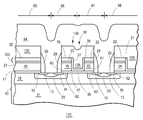
- FIG. 1 schematically illustrates an enlarged cross-sectional portion of a semiconductor device 10 that has a low gate-to-drain capacitance (Cgd) and that has a low ratio between the gate-to-drain and gate-to-source capacitance (Qgd/Qgs(th)) which facilitates high frequency operation and minimizes shoot-through currents.
- Cgd gate-to-drain capacitance
- Qgd/Qgs(th) gate-to-source capacitance
- FIG. 2 schematically illustrates an enlarged plan view of a portion of a topology of an embodiment of device 10 .
- the plan view of FIG. 2 excludes a source conductor 64 in order to illustrate the underlying elements of device 10 .
- the view of FIG. 1 is taken along a section line 1 - 1 of FIG. 2 .
- the following description has references to both FIG. 1 and FIG. 2 .
- MOS transistor structures including a first transistor stripe or transistor 65 , a second transistor stripe or transistor 66 , a third transistor stripe or transistor 67 , and a fourth transistor stripe or transistor 68 that are formed in a stripe configuration, for example a configuration having body regions formed as a plurality of elongated regions with each body region having a plurality of transistor sources.
- Transistors 65 , 66 , 67 , and 68 are identified in a general manner by arrows.
- Device 10 has an N-type semiconductor substrate 50 that includes an N-type bulk semiconductor substrate 11 on which a N-type epitaxial layer 12 is formed.
- N-type sources 14 , 15 , and 16 are formed within P-type body regions 13 . Heavily doped P-type regions 23 within body regions 13 facilitate forming low resistance electrical contact to body regions 13 .
- a gate structure 30 for transistors 66 and 67 is formed overlying a surface 36 of substrate 50 with at least a first edge 60 of structure 30 overlying at least an edge of source 14 and at least a second edge 61 of structure 30 overlying at least an edge of source 15 . Edges 60 and 61 generally overlie respective sources 14 and 15 about one-tenth to one-half (0.1 to 0.5) microns.
- gate structure 30 has a conductor plug that includes an insulator 27 that is formed on at least sidewalls of an opening 32 that is formed within gate structure 30 , and a conductor 26 that is formed on insulator 27 . Conductor 26 is electrically connected to a source conductor 64 .
- opening 32 is formed in gate structure 30 so that opening 32 overlies a portion of substrate 50 that is positioned in-between source 14 and source region 15 and preferably is positioned in-between regions 13 in which sources 14 and 15 are formed.
- Gate structure 30 and opening 32 are identified in a general manner by arrows.
- Other transistors of device 10 such as transistors 65 and 68 , have gate structures similar to structure 30 as illustrated in FIG. 1 .
- a portion of regions 13 that is underlying gate structure 30 and similar adjacent gate structures forms channel regions 62 of transistors 65 , 66 , 67 , and 68 . Also a portion of substrate 50 underlying gate structure 30 and similar adjacent gate structures forms a drain region of transistors 65 , 66 , 67 , and 68 .
- the voltage spike that is coupled to the gate of a transistor when the drain electrode is pulled high is desirable to minimize the voltage spike that is coupled to the gate of a transistor when the drain electrode is pulled high.
- One way to achieve this is to reduce the coupling between the drain and gate by reducing the gate to drain capacitance (Cgd), which also reduces the gate to drain charge (Qgd).
- Cgd gate to drain capacitance
- Qgd gate to drain charge
- the ratio of the gate-to-drain charge (Qgd) to the gate-to-source charge that is required induce a voltage equal to Vth (Qgs(th)) should be less than 1 (Qgd/Qgs(th) ⁇ 1). It is also desirable to have a low total gate charge in order to improve the operating frequency.
- Reducing the gate-to-drain capacitance reduces the gate-to-drain charge (Qgd) and reducing the gate-to-source capacitance reduces the gate-to-source charge (Qgs).
- forming conductor 26 within opening 32 assists in reducing the gate-to-drain capacitance (Cgd) of device 10 .
- Minimizing the amount of gates 18 and 19 that overlie the drain of device 10 also assists in reducing the gate-to-drain capacitance, thus, the gate-to-drain charge (Qgd) of device 10 .
- conductor 26 assists in further reducing the gate-to-drain capacitance, by causing a portion of the charge in the drain region to be coupled to the source, instead of to the gate.
- Conductor 26 is formed within opening 32 , and is removed from a top surface 35 of structure 30 . Reducing the gate-to-drain charge also reduces the gate charge ratio (Qgd/Qgs(th)) thereby minimizing the false turn-on of device 10 . It is believed that device 10 has a gate charge ratio (Qgd/Qgs(th)) that is below one (1) which is much less than the gate charge ratio of two to four of prior art power devices. Reducing the gate-drain charge also reduces the total gate charge thereby increasing the operating frequency of device 10 .
- FIG. 3-FIG . 6 schematically illustrate various stages according to an embodiment of a method of forming device 10 .
- This description has references to FIGS. 1-6 .
- the description of FIGS. 3-6 illustrates the portion of device 10 illustrated in FIG. 1 .
- device 10 is illustrated with specific conductivity types for an N-channel device, the conductivity types may be reversed to provide a P-channel device.
- device 10 is illustrated to show either a stripe design (where the body regions are a plurality of elongated regions) or a single body region design that typically is formed in an elongated pattern or a serpentine pattern.
- the present invention encompasses either a stripe design, a closed cell design, a multiple cell design, or a single body design.
- device 10 is formed on a bulk N-type semiconductor substrate 11 which has an N-type epitaxial layer 12 formed on a surface thereof.
- Substrate 11 and layer 12 comprise semiconductor substrate 50 .
- a gate insulator layer 17 is formed on a portion of surface 36 of substrate 50 where transistors 65 - 68 are being formed.
- the resistivity of substrate 11 is about 0.001 to 0.01 ohm-cm and the resistivity of layer 12 is approximately 0.1 to 10 ohm-cm.
- gate insulator layer 17 is a layer of silicon dioxide having a thickness of approximately one hundred (100) to eight hundred (800) angstroms.
- a gate conductor layer 28 is formed on layer 17 overlying at least a portion of substrate 50 where transistors 65 - 68 are being formed.
- Gate conductor layer 28 typically is a conductor material such as a refractory metal, a refractory metal silicide, a refractory metal salicide, or doped poly-crystalline silicon (doped polysilicon).
- layer 28 is N-type polysilicon having a sheet resistance of at least approximately one hundred (100) ohm/sq and preferably about ten to thirty (10 to 30) ohm/sq.
- a protective insulating layer 25 is formed on gate conductor layer 28 to insulate layer 28 from other conductors that will subsequently be formed.
- insulating layer 25 is a silicon dioxide layer, deposited to a thickness of about three thousand to ten thousand (3000-10,000) angstroms.
- insulating layer 25 includes a silicon dioxide layer 21 that is formed on layer 28 and a silicon nitride layer 22 that is formed on layer 21 .
- layer 25 may also include another silicon dioxide layer that is formed on layer 22 .
- the thickness of layer 25 keeps source conductor 64 (See FIG. 1 ) sufficiently far from gates 18 and 19 to reduce the gate-to-source capacitance of device 10 .
- Layer 21 typically has a thickness of about three thousand to ten thousand (3000-10000) angstroms and layer 22 has a thickness of about two hundred to fifteen hundred (200-1500) angstroms.
- Other insulators may also be used for layer 25 .
- a mask (illustrated by dashed lines) is applied on the surface of layer 25 and patterned to expose the desired portions of layer 25 where opening 32 is to be formed. Opening 32 is formed through the openings in the mask to extend from the surface of layer 25 , through layer 28 to expose a portion of layer 17 . In some embodiments, opening 32 may extend into or through layer 17 . The width of opening 32 can be as wide as possible as long as opening 32 does not overlie regions 13 . In some embodiments, an optional doped region 41 may also be formed as a doped region on the surface of substrate 50 and extending into substrate 50 underlying opening 32 .
- Region 41 may be doped P-type to form a capacitance shield area to further reduce the gate-to-drain capacitance of device 10 , or it may be doped N-type to further reduce the Rds(on) of device 10 .
- Optional doped region 41 is illustrated by a dashed line.
- an insulator 27 is formed on the sidewalls of opening 32 thus on the sidewalls of gate structure 30 .
- Insulator 27 insulates gates 18 and 19 (see FIG. 1 ) from conductor 26 .
- Insulator 27 forms a dielectric of a capacitor that causes a portion of the charge in the drain region to be coupled to the source, instead of the gate.
- insulator 27 is a layer of silicon dioxide that is deposited along the sidewalls of gate structure 30 , onto the portion of gate insulator layer 17 that is exposed within opening 32 , and not on surface 35 .
- the silicon dioxide layer generally has a thickness of about one hundred to one thousand (100-1000) angstroms.
- layer 27 includes a silicon dioxide layer that is formed on the sidewalls of gate structure 30 and on top of gate insulator 17 , and a silicon nitride layer that is formed on the silicon dioxide layer. Using both the silicon dioxide layer and the silicon nitride layer facilitates increasing the dielectric constant of layer 27 . This allows the use of a thicker insulating layer 27 , which reduces the incidence of shorts between gate structure 30 , and subsequently deposited conductor 26 .
- the silicon dioxide layer typically has a thickness of about one hundred to five hundred (100-500) angstroms and the silicon nitride layer typically has a thickness of about two hundred to fifteen hundred (200-1500) angstroms.
- insulator 27 may also be formed on surface 35 .
- conductor 26 is formed to fill the remainder of opening 32 .
- the material used for conductor 26 can be any of a variety of conductor materials including a refractory metal, a refractory metal silicide, a refractory metal salicide, or doped poly-crystalline silicon (doped polysilicon).
- conductor 26 is N-type polysilicon having a doping concentration of at least 1E18 ohm-cm in order to provide a sheet resistance of at least approximately two thousand (2000) ohm/sq and preferably about ten to one hundred (10 to 100) ohm/sq.
- conductor 26 is formed with a thickness sufficient to at least fill opening 32 so that a portion of conductor 26 is substantially coplanar to surface 35 .
- conductor 26 is applied to a thickness sufficient to fill all of opening 32 but not to extend past surface 35 .
- a planarization process usually is utilized to remove all the material of conductor 26 that extends past surface 35 .
- a chemical-mechanical planarization process CMP
- an RIE etch-back CMP
- the goal is to remove substantially all of conductor 26 that extends past surface 35 such that conductor 26 is substantially coplanar with surface 35 . Due to processing variations a portion of conductor 26 may be slightly recessed below surface 35 .
- openings 31 and 33 are formed in layer 25 and layer 28 .
- a mask (not shown) is applied onto the surface of layer 25 and patterned to expose the desired portions of layer 25 where openings 31 and 33 are to be formed. Openings 31 and 33 are formed through the openings in the mask to extend from the surface of layer 25 through layer 28 to expose layer 17 . Openings 31 and 33 are used to dope the first and second portion of substrate 50 to form body regions 13 extending from first surface 36 of substrate 50 a first distance into substrate 50 . Regions 13 typically are formed by ion implantation and activation techniques that are well known to those skilled in the art. Openings 31 and 33 form portions of layers 28 and 25 into gate structure 30 that forms the gate of transistors 66 and 67 .
- Opening 32 forms gate structure 30 into a first gate section that includes first gate 18 that is a first portion of gate conductor layer 28 and the overlying portions of layer 25 , and into a second gate section that includes second gate 19 of gate conductor layer 28 and the overlying portions of layer 25 .
- the first gate section functions as the gate of transistor 66
- the second gate section functions as the gate of transistor 67 .
- Opening 32 and the conductor plug minimize the amount of gate structure 30 overlying the drain portion of transistors 47 and 48 thereby minimizing the gate-to-drain capacitance (Cgd) of device 10 . It has been found that conductor 26 within opening 32 also reduces Cgd.
- the gate-to-drain charge (Qgd) of device 10 is about forty percent (40%) less that in the prior art.
- Opening 32 , top surface 35 of structure 30 , and the conductor plug typically extend in a general manner laterally across substrate 50 and laterally overlying surface 36 according to the layout pattern selected for gate structure 30 . See FIG. 2 for one example of a layout topology for device 10 with the conductor plug and opening 32 extending laterally across substrate 50 .
- surface 35 typically is substantially parallel to surface 36 . However, those skilled in the art realize that surface 35 generally is not exactly parallel to surface 36 but may have an irregular surface due to processing of underlying elements of device 10 .
- N-type sources 14 , 15 , and 16 are formed within body regions 13 .
- a mask layer such as photo-resist, is applied to device 10 and patterned to leave blocking portions 51 within openings 31 and 33 .
- the mask layer is not shown in FIG. 3 for clarity of the drawings.
- portion 51 within opening 31 may extend across surface 36 to the side of layer 28 to prevent forming a source region in the underlying portion of region 13 .
- Sources 14 , 15 , and 16 are formed by doping the surface of substrate 50 through openings 31 and 33 and around blocking portions 51 by techniques that are well known to those skilled in the art.
- spacers 29 are formed within openings 31 and 33 along the sidewalls of openings 31 and 33 and extending a first distance across the underlying portion of surface 36 .
- Spacers 29 are formed by techniques that are well known to those skilled in the art.
- spacers 29 may be formed by applying a spacer dielectric layer, not shown, such as TEOS covering device 10 and including openings 31 and 33 .
- An anisotropic etch can be used to remove portions of the spacer dielectric layer from surface 36 of substrate 50 , and surface 35 of gate structure 30 and the top surface of conductor plug 26 , and leave portions of the spacer dielectric layer as spacers 29 .
- the portion of substrate 50 exposed within openings 31 and 33 is doped to form heavily doped P-regions 23 .
- Spacers 29 are used to protect portions of sources 14 - 16 while forming regions 23 within regions 13 and abutting respective sources 14 , 15 , and 16 .
- a source conductor 64 is applied within openings 31 and 33 and across onto gate structure 30 . Conductor 64 forms electrical contact to sources 14 - 16 , heavily doped P-regions 23 , and conductor 26 .
- FIG. 7 schematically illustrates a portion of an embodiment of semiconductor device 110 that is an alternate embodiment of device 10 explained in the description of FIGS. 1-6 .
- Device 110 is similar to device 10 , except that conductor 26 of device 10 is extended onto surface 35 to form conductor 126 thereby forming a gate structure 130 that is similar to structure 30 except for replacing conductor 26 with conductor 126 .
- layer 25 is replaced with a layer 125 .
- Layer 125 is the same materials as layer 25 but is thinner.
- Using both silicon dioxide layer 21 and silicon nitride layer 22 to insulate layer 28 facilitates increasing the dielectric constant of the gate-to-source capacitor that includes portions of layer 22 .
- Conductor 126 increases the gate-to-source capacitance of device 110 thereby decreasing the gate charge ratio (Qgd/Qgs(th)) of device 110 .
- Conductor 126 is formed similarly to conductor 26 except that conductor 126 is formed on surface 35 and is not removed from surface 35 in order to form conductor 126 .
- opening 32 may be formed in layer 28 prior to forming layer 125 .
- Layer 125 may be formed on layer 28 , along the sidewalls of opening 32 , and on the exposed portions of layer 17 within opening 32 . Since layer 125 in device is thinner than layer 25 in device 10 , the gate to source capacitance of device 110 is increased further, resulting in a lower Qgd/Qgs(th) ratio.
- FIG. 8 schematically illustrates a portion of an embodiment of semiconductor device 210 that is an alternate embodiment of device 10 explained in the description of FIGS. 1-6 .
- Device 210 includes a gate structure 230 .
- Gate structure 230 is similar to structure 30 except that opening 32 is not formed in structure 230 .
- Insulator layer 25 is formed on gate layer 28 . Consequently, device 210 does not have insulator 27 , and conductor 26 is not formed within opening 32 . Instead, a conductor 226 is formed on surface 35 of layer 25 .
- the material of conductor 226 is the same as the material of conductor 26 .
- the thickness of conductor 226 is selected to be about two thousand to ten thousand (2000-10,000) angstroms.
- Conductor 226 increases the gate-to-source capacitance of device 210 thereby decreasing the gate charge ratio. Conductor 226 also increases the height of gate structure 230 , thus facilitating the formation of spacers 29 .
- Device 210 is formed similarly to device 10 , except that opening 32 and insulator 27 are omitted, and conductor 26 is formed on surface 35 to form conductor 226 . In some applications it is important to reduce the shoot-through currents even if the gate-to-source capacitance may be increased.
- a novel device and method is disclosed. Included, among other features, is forming semiconductor device having a conductor plug extending into or through the gate structure.
- the conductor plug reduces the gate-to-drain capacitance facilitating higher operating frequencies and reduces the gate charge ratio thereby reducing shoot-through currents.
- forming a conductor on the gate structure with an underlying thin insulator increases the gate-to-source capacitance which reduces the gate charge ratio and reduces shoot-through currents.
Abstract
Description
Claims (4)
Priority Applications (1)
| Application Number | Priority Date | Filing Date | Title |
|---|---|---|---|
| US12/574,934 US7851852B2 (en) | 2004-09-16 | 2009-10-07 | Method of forming a low capacitance semiconductor device and structure therefor |
Applications Claiming Priority (3)
| Application Number | Priority Date | Filing Date | Title |
|---|---|---|---|
| US10/942,060 US7192814B2 (en) | 2004-09-16 | 2004-09-16 | Method of forming a low capacitance semiconductor device and structure therefor |
| US11/671,664 US7619287B2 (en) | 2004-09-16 | 2007-02-06 | Method of forming a low capacitance semiconductor device and structure therefor |
| US12/574,934 US7851852B2 (en) | 2004-09-16 | 2009-10-07 | Method of forming a low capacitance semiconductor device and structure therefor |
Related Parent Applications (1)
| Application Number | Title | Priority Date | Filing Date |
|---|---|---|---|
| US11/671,664 Continuation US7619287B2 (en) | 2004-09-16 | 2007-02-06 | Method of forming a low capacitance semiconductor device and structure therefor |
Publications (2)
| Publication Number | Publication Date |
|---|---|
| US20100025745A1 US20100025745A1 (en) | 2010-02-04 |
| US7851852B2 true US7851852B2 (en) | 2010-12-14 |
Family
ID=36033033
Family Applications (3)
| Application Number | Title | Priority Date | Filing Date |
|---|---|---|---|
| US10/942,060 Active 2024-11-30 US7192814B2 (en) | 2004-09-16 | 2004-09-16 | Method of forming a low capacitance semiconductor device and structure therefor |
| US11/671,664 Active 2026-02-28 US7619287B2 (en) | 2004-09-16 | 2007-02-06 | Method of forming a low capacitance semiconductor device and structure therefor |
| US12/574,934 Active US7851852B2 (en) | 2004-09-16 | 2009-10-07 | Method of forming a low capacitance semiconductor device and structure therefor |
Family Applications Before (2)
| Application Number | Title | Priority Date | Filing Date |
|---|---|---|---|
| US10/942,060 Active 2024-11-30 US7192814B2 (en) | 2004-09-16 | 2004-09-16 | Method of forming a low capacitance semiconductor device and structure therefor |
| US11/671,664 Active 2026-02-28 US7619287B2 (en) | 2004-09-16 | 2007-02-06 | Method of forming a low capacitance semiconductor device and structure therefor |
Country Status (5)
| Country | Link |
|---|---|
| US (3) | US7192814B2 (en) |
| KR (1) | KR101271066B1 (en) |
| CN (1) | CN1808708B (en) |
| HK (1) | HK1092279A1 (en) |
| TW (1) | TWI379389B (en) |
Families Citing this family (5)
| Publication number | Priority date | Publication date | Assignee | Title |
|---|---|---|---|---|
| US20030125768A1 (en) * | 2000-02-11 | 2003-07-03 | Forsell Peter | Impotence treatment apparatus with energy transforming means |
| CN101593695B (en) * | 2008-05-30 | 2011-06-15 | 中芯国际集成电路制造(上海)有限公司 | Method for solving power field effect tube wafer bending |
| US20120150955A1 (en) * | 2010-12-10 | 2012-06-14 | Erick Tseng | Contact Resolution Using Social Graph Information |
| CN102738229B (en) * | 2011-03-31 | 2015-01-28 | 无锡维赛半导体有限公司 | Structure of power transistor and method for manufacturing power transistor |
| CN108565289A (en) * | 2018-06-26 | 2018-09-21 | 南京方旭智芯微电子科技有限公司 | The manufacturing method of superjunction field-effect tube and superjunction field-effect tube |
Citations (14)
| Publication number | Priority date | Publication date | Assignee | Title |
|---|---|---|---|---|
| JPS5984474A (en) | 1982-11-05 | 1984-05-16 | Nec Corp | Vertical type field effect transistor for power |
| EP0067475B1 (en) | 1981-06-17 | 1987-03-11 | Philips Electronics Uk Limited | Insulated gate field effect transistor and its manufacture |
| EP0112607B1 (en) | 1982-09-03 | 1987-03-18 | Western Electric Company, Incorporated | Power mos transistor |
| JPH01111378A (en) | 1987-10-26 | 1989-04-28 | Nippon Telegr & Teleph Corp <Ntt> | Vertical mosfet |
| US5631484A (en) | 1995-12-26 | 1997-05-20 | Motorola, Inc. | Method of manufacturing a semiconductor device and termination structure |
| US5998833A (en) | 1998-10-26 | 1999-12-07 | North Carolina State University | Power semiconductor devices having improved high frequency switching and breakdown characteristics |
| US6107160A (en) | 1997-08-04 | 2000-08-22 | Spectrian Corporation | MOSFET having buried shield plate for reduced gate/drain capacitance |
| US6197640B1 (en) | 1998-12-21 | 2001-03-06 | Semiconductor Components Industries, Llc | Semiconductor component and method of manufacture |
| US6222229B1 (en) | 1999-02-18 | 2001-04-24 | Cree, Inc. | Self-aligned shield structure for realizing high frequency power MOSFET devices with improved reliability |
| US20020140042A1 (en) | 2001-03-28 | 2002-10-03 | International Rectifier Corporation | Ultra low QGD power MOSFET |
| US6525372B2 (en) | 2000-11-16 | 2003-02-25 | Silicon Wireless Corporation | Vertical power devices having insulated source electrodes in discontinuous deep trenches |
| US6621121B2 (en) | 1998-10-26 | 2003-09-16 | Silicon Semiconductor Corporation | Vertical MOSFETs having trench-based gate electrodes within deeper trench-based source electrodes |
| US6683346B2 (en) | 2001-03-09 | 2004-01-27 | Fairchild Semiconductor Corporation | Ultra dense trench-gated power-device with the reduced drain-source feedback capacitance and Miller charge |
| US20040108547A1 (en) | 2002-12-09 | 2004-06-10 | Semiconductor Components Industries, Llc. | Power switching transistor with low drain to gate capacitance |
-
2004
- 2004-09-16 US US10/942,060 patent/US7192814B2/en active Active
-
2005
- 2005-09-15 TW TW094131863A patent/TWI379389B/en active
- 2005-09-16 CN CN2005101315442A patent/CN1808708B/en not_active Expired - Fee Related
- 2005-09-16 KR KR1020050087038A patent/KR101271066B1/en active IP Right Grant
-
2006
- 2006-11-15 HK HK06112545.9A patent/HK1092279A1/en not_active IP Right Cessation
-
2007
- 2007-02-06 US US11/671,664 patent/US7619287B2/en active Active
-
2009
- 2009-10-07 US US12/574,934 patent/US7851852B2/en active Active
Patent Citations (16)
| Publication number | Priority date | Publication date | Assignee | Title |
|---|---|---|---|---|
| EP0067475B1 (en) | 1981-06-17 | 1987-03-11 | Philips Electronics Uk Limited | Insulated gate field effect transistor and its manufacture |
| EP0112607B1 (en) | 1982-09-03 | 1987-03-18 | Western Electric Company, Incorporated | Power mos transistor |
| JPS5984474A (en) | 1982-11-05 | 1984-05-16 | Nec Corp | Vertical type field effect transistor for power |
| JPH01111378A (en) | 1987-10-26 | 1989-04-28 | Nippon Telegr & Teleph Corp <Ntt> | Vertical mosfet |
| US5631484A (en) | 1995-12-26 | 1997-05-20 | Motorola, Inc. | Method of manufacturing a semiconductor device and termination structure |
| US6107160A (en) | 1997-08-04 | 2000-08-22 | Spectrian Corporation | MOSFET having buried shield plate for reduced gate/drain capacitance |
| US6621121B2 (en) | 1998-10-26 | 2003-09-16 | Silicon Semiconductor Corporation | Vertical MOSFETs having trench-based gate electrodes within deeper trench-based source electrodes |
| US6388286B1 (en) | 1998-10-26 | 2002-05-14 | North Carolina State University | Power semiconductor devices having trench-based gate electrodes and field plates |
| US5998833A (en) | 1998-10-26 | 1999-12-07 | North Carolina State University | Power semiconductor devices having improved high frequency switching and breakdown characteristics |
| US6197640B1 (en) | 1998-12-21 | 2001-03-06 | Semiconductor Components Industries, Llc | Semiconductor component and method of manufacture |
| US6222229B1 (en) | 1999-02-18 | 2001-04-24 | Cree, Inc. | Self-aligned shield structure for realizing high frequency power MOSFET devices with improved reliability |
| US6525372B2 (en) | 2000-11-16 | 2003-02-25 | Silicon Wireless Corporation | Vertical power devices having insulated source electrodes in discontinuous deep trenches |
| US6649975B2 (en) | 2000-11-16 | 2003-11-18 | Silicon Semiconductor Corporation | Vertical power devices having trench-based electrodes therein |
| US6683346B2 (en) | 2001-03-09 | 2004-01-27 | Fairchild Semiconductor Corporation | Ultra dense trench-gated power-device with the reduced drain-source feedback capacitance and Miller charge |
| US20020140042A1 (en) | 2001-03-28 | 2002-10-03 | International Rectifier Corporation | Ultra low QGD power MOSFET |
| US20040108547A1 (en) | 2002-12-09 | 2004-06-10 | Semiconductor Components Industries, Llc. | Power switching transistor with low drain to gate capacitance |
Also Published As
| Publication number | Publication date |
|---|---|
| KR101271066B1 (en) | 2013-06-04 |
| TW200623372A (en) | 2006-07-01 |
| TWI379389B (en) | 2012-12-11 |
| CN1808708A (en) | 2006-07-26 |
| HK1092279A1 (en) | 2007-02-02 |
| US20070128811A1 (en) | 2007-06-07 |
| US20060055025A1 (en) | 2006-03-16 |
| US20100025745A1 (en) | 2010-02-04 |
| US7192814B2 (en) | 2007-03-20 |
| KR20060051408A (en) | 2006-05-19 |
| US7619287B2 (en) | 2009-11-17 |
| CN1808708B (en) | 2012-05-30 |
Similar Documents
| Publication | Publication Date | Title |
|---|---|---|
| US9306018B2 (en) | Trench shielding structure for semiconductor device and method | |
| US10355125B2 (en) | Electrode contact structure for semiconductor device | |
| US8362548B2 (en) | Contact structure for semiconductor device having trench shield electrode and method | |
| US7915672B2 (en) | Semiconductor device having trench shield electrode structure | |
| US9450091B2 (en) | Semiconductor device with enhanced mobility and method | |
| CN203325907U (en) | Insulated gate semiconductor device structure | |
| US7663186B2 (en) | Semiconductor device | |
| US11721738B2 (en) | Laterally diffused metal oxide semiconductor with gate poly contact within source window | |
| US20020074585A1 (en) | Self-aligned power MOSFET with enhanced base region | |
| US20030057459A1 (en) | High current field-effect transistor | |
| US7768078B2 (en) | Power semiconductor device having improved performance and method | |
| KR20010112439A (en) | A super-self-aligned trench-gate dmos with reduced on-resistance | |
| US8921184B2 (en) | Method of making an electrode contact structure and structure therefor | |
| US20070215914A1 (en) | Power semiconductor device having improved performance and method | |
| US7851852B2 (en) | Method of forming a low capacitance semiconductor device and structure therefor | |
| US20230223474A1 (en) | Insulated gated field effect transistor structure having shielded source and method | |
| US20010023957A1 (en) | Trench-gate semiconductor devices | |
| US20020195654A1 (en) | DMOS transistor and fabricating method thereof | |
| JP2003051594A (en) | Semiconductor device and manufacturing method therefor | |
| US10784373B1 (en) | Insulated gated field effect transistor structure having shielded source and method | |
| US20050139858A1 (en) | Lateral double-diffused MOS transistor device |
Legal Events
| Date | Code | Title | Description |
|---|---|---|---|
| AS | Assignment |
Owner name: JPMORGAN CHASE BANK, N.A., AS COLLATERAL AGENT,NEW Free format text: SECURITY AGREEMENT;ASSIGNOR:SEMICONDUCTOR COMPONENTS INDUSTRIES, LLC;REEL/FRAME:024094/0429 Effective date: 20100311 Owner name: JPMORGAN CHASE BANK, N.A., AS COLLATERAL AGENT, NE Free format text: SECURITY AGREEMENT;ASSIGNOR:SEMICONDUCTOR COMPONENTS INDUSTRIES, LLC;REEL/FRAME:024094/0429 Effective date: 20100311 |
|
| STCF | Information on status: patent grant |
Free format text: PATENTED CASE |
|
| FPAY | Fee payment |
Year of fee payment: 4 |
|
| AS | Assignment |
Owner name: DEUTSCHE BANK AG NEW YORK BRANCH, NEW YORK Free format text: SECURITY INTEREST;ASSIGNOR:SEMICONDUCTOR COMPONENTS INDUSTRIES, LLC;REEL/FRAME:038620/0087 Effective date: 20160415 |
|
| AS | Assignment |
Owner name: SEMICONDUCTOR COMPONENTS INDUSTRIES, LLC, ARIZONA Free format text: RELEASE BY SECURED PARTY;ASSIGNOR:JPMORGAN CHASE BANK, N.A. (ON ITS BEHALF AND ON BEHALF OF ITS PREDECESSOR IN INTEREST, CHASE MANHATTAN BANK);REEL/FRAME:038632/0074 Effective date: 20160415 Owner name: SEMICONDUCTOR COMPONENTS INDUSTRIES, LLC, ARIZONA Free format text: RELEASE BY SECURED PARTY;ASSIGNOR:JPMORGAN CHASE BANK, N.A., AS ADMINISTRATIVE AGENT AND COLLATERAL AGENT;REEL/FRAME:038631/0345 Effective date: 20100511 |
|
| AS | Assignment |
Owner name: DEUTSCHE BANK AG NEW YORK BRANCH, AS COLLATERAL AGENT, NEW YORK Free format text: CORRECTIVE ASSIGNMENT TO CORRECT THE INCORRECT PATENT NUMBER 5859768 AND TO RECITE COLLATERAL AGENT ROLE OF RECEIVING PARTY IN THE SECURITY INTEREST PREVIOUSLY RECORDED ON REEL 038620 FRAME 0087. ASSIGNOR(S) HEREBY CONFIRMS THE SECURITY INTEREST;ASSIGNOR:SEMICONDUCTOR COMPONENTS INDUSTRIES, LLC;REEL/FRAME:039853/0001 Effective date: 20160415 Owner name: DEUTSCHE BANK AG NEW YORK BRANCH, AS COLLATERAL AG Free format text: CORRECTIVE ASSIGNMENT TO CORRECT THE INCORRECT PATENT NUMBER 5859768 AND TO RECITE COLLATERAL AGENT ROLE OF RECEIVING PARTY IN THE SECURITY INTEREST PREVIOUSLY RECORDED ON REEL 038620 FRAME 0087. ASSIGNOR(S) HEREBY CONFIRMS THE SECURITY INTEREST;ASSIGNOR:SEMICONDUCTOR COMPONENTS INDUSTRIES, LLC;REEL/FRAME:039853/0001 Effective date: 20160415 |
|
| MAFP | Maintenance fee payment |
Free format text: PAYMENT OF MAINTENANCE FEE, 8TH YEAR, LARGE ENTITY (ORIGINAL EVENT CODE: M1552) Year of fee payment: 8 |
|
| MAFP | Maintenance fee payment |
Free format text: PAYMENT OF MAINTENANCE FEE, 12TH YEAR, LARGE ENTITY (ORIGINAL EVENT CODE: M1553); ENTITY STATUS OF PATENT OWNER: LARGE ENTITY Year of fee payment: 12 |
|
| AS | Assignment |
Owner name: FAIRCHILD SEMICONDUCTOR CORPORATION, ARIZONA Free format text: RELEASE OF SECURITY INTEREST IN PATENTS RECORDED AT REEL 038620, FRAME 0087;ASSIGNOR:DEUTSCHE BANK AG NEW YORK BRANCH, AS COLLATERAL AGENT;REEL/FRAME:064070/0001 Effective date: 20230622 Owner name: SEMICONDUCTOR COMPONENTS INDUSTRIES, LLC, ARIZONA Free format text: RELEASE OF SECURITY INTEREST IN PATENTS RECORDED AT REEL 038620, FRAME 0087;ASSIGNOR:DEUTSCHE BANK AG NEW YORK BRANCH, AS COLLATERAL AGENT;REEL/FRAME:064070/0001 Effective date: 20230622 |