US7823099B2 - Lithography suspect spot location and scoring system - Google Patents

Lithography suspect spot location and scoring system Download PDF

Info

Publication number
US7823099B2
US7823099B2 US11/756,596 US75659607A US7823099B2 US 7823099 B2 US7823099 B2 US 7823099B2 US 75659607 A US75659607 A US 75659607A US 7823099 B2 US7823099 B2 US 7823099B2
Authority
US
United States
Prior art keywords
sensitive
spots
key area
design
scoring
Prior art date
Legal status (The legal status is an assumption and is not a legal conclusion. Google has not performed a legal analysis and makes no representation as to the accuracy of the status listed.)
Active, expires
Application number
US11/756,596
Other versions
US20080301623A1 (en
Inventor
Min-Chun Tsai
Charles C. Chiang
Current Assignee (The listed assignees may be inaccurate. Google has not performed a legal analysis and makes no representation or warranty as to the accuracy of the list.)
Synopsys Inc
Original Assignee
Synopsys Inc
Priority date (The priority date is an assumption and is not a legal conclusion. Google has not performed a legal analysis and makes no representation as to the accuracy of the date listed.)
Filing date
Publication date
Application filed by Synopsys Inc filed Critical Synopsys Inc
Priority to US11/756,596 priority Critical patent/US7823099B2/en
Assigned to SYNOPSYS, INC. reassignment SYNOPSYS, INC. ASSIGNMENT OF ASSIGNORS INTEREST (SEE DOCUMENT FOR DETAILS). Assignors: CHIANG, CHARLES C., MR., TSAI, MIN-CHUN, MR.
Publication of US20080301623A1 publication Critical patent/US20080301623A1/en
Application granted granted Critical
Publication of US7823099B2 publication Critical patent/US7823099B2/en
Active legal-status Critical Current
Adjusted expiration legal-status Critical

Links

Images

Classifications

    • GPHYSICS
    • G06COMPUTING; CALCULATING OR COUNTING
    • G06FELECTRIC DIGITAL DATA PROCESSING
    • G06F30/00Computer-aided design [CAD]
    • G06F30/30Circuit design
    • G06F30/39Circuit design at the physical level
    • G06F30/398Design verification or optimisation, e.g. using design rule check [DRC], layout versus schematics [LVS] or finite element methods [FEM]
    • GPHYSICS
    • G06COMPUTING; CALCULATING OR COUNTING
    • G06FELECTRIC DIGITAL DATA PROCESSING
    • G06F2119/00Details relating to the type or aim of the analysis or the optimisation
    • G06F2119/18Manufacturability analysis or optimisation for manufacturability
    • YGENERAL TAGGING OF NEW TECHNOLOGICAL DEVELOPMENTS; GENERAL TAGGING OF CROSS-SECTIONAL TECHNOLOGIES SPANNING OVER SEVERAL SECTIONS OF THE IPC; TECHNICAL SUBJECTS COVERED BY FORMER USPC CROSS-REFERENCE ART COLLECTIONS [XRACs] AND DIGESTS
    • Y02TECHNOLOGIES OR APPLICATIONS FOR MITIGATION OR ADAPTATION AGAINST CLIMATE CHANGE
    • Y02PCLIMATE CHANGE MITIGATION TECHNOLOGIES IN THE PRODUCTION OR PROCESSING OF GOODS
    • Y02P90/00Enabling technologies with a potential contribution to greenhouse gas [GHG] emissions mitigation
    • Y02P90/02Total factory control, e.g. smart factories, flexible manufacturing systems [FMS] or integrated manufacturing systems [IMS]

Definitions

  • the invention relates to design of semiconductor chips. More specifically, the invention relates to a method and an apparatus for improving lithography printability for integrated circuits.
  • Lithography which allows selective removal portions of a thin film such as photoresist, is a key process used in the fabrication of integrated circuits. Specifically, a photomask with the desired geometric pattern is created. Then, a light source passes through the photomask to transfer the geometric pattern on the thin film, which covers a substrate. The portions of the thin film that received light through the photomask are chemically altered by the light so that later process steps can remove these portions of the thin film to expose selected portions of the substrate. The substrate is then further processed to create the features of the integrated circuit.
  • lithography techniques could easily transfer the geometric pattern of the photomask to the thin film.
  • optical constraints in lithography processes has become a limiting factor of the feature size of semiconductor devices.
  • Advancement in lithography allows feature sizes to be smaller than the wavelength of light used in the lithography pattern.
  • the geometric pattern of the photomask does not transfer cleanly to the thin film. For example, as illustrated in FIG. 1( a ), a rectangle 115 in a photomask 110 may result in a peanut shape 125 on thin film 120 .
  • lithography steppers are limited to a critical dimension CD that is equal to a process factor (K 1 ) multiplied by the frequency of the light used by the stepper ( ⁇ ) divided by the numerical aperture (NA) (as show in Equation EQ1).
  • CD ( K 1* ⁇ )/ NA (EQ1)
  • Lithography technology in 2007 uses deep ultraviolet light, which has a wavelength of 193 nm.
  • the numerical aperture NA has a upper limit of 0.85 which can be increased using immersion technology to about 1.3-1.4.
  • RET resolution enhancement techniques
  • portions of the geometric pattern is reshaped to compensate for the deformity from the lithography process.
  • a reshaped polygon 135 (based on rectangle 115 of FIG. 1( a ) with enhanced corners and sides) in a photomask 130 results in a near rectangular shape 145 on thin film 140 .
  • Near rectangular shape 145 approximates rectangle 115 more closely than peanut shape 125 .
  • RET/OPC can be used to improve the quality of the geometric pattern produced on the thin film and thus provides a better process factor K 1 .
  • RET/OPC require very complicated design rules.
  • design rule technology in general can not adequately describe the complicated constraints of RET/OPC.
  • the integrated circuit manufactured from the design may still have “hot spots”, i.e. areas which would cause failure of the integrated circuit.
  • excessive design rules are created for use with RET/OPC techniques to minimize the chances of hot spots in the fabricated devices.
  • the excessive design rules are likely to lead to false violations, which would greatly increase the design time required for integrated circuits to address all the false violations.
  • hot spot detection and correction may be delayed until after RET/OPC.
  • the post RET/OPC hot spot detection and correction would require detailed information about the RET/OPC process that is used by each foundry.
  • each new generation of RET/OPC techniques may require years of development.
  • IC development and design typically occurs long before the RET/OPC techniques are certified.
  • simulation required to perform the post RET/OPC hot spot detection and correction is extremely time consuming and can greatly delay the IC design.
  • a method and apparatus for rapidly detecting potential hot spots (sensitive spots) in an IC design is a method and apparatus for rapidly detecting potential hot spots (sensitive spots) in an IC design.
  • the present invention provides a fast method to detect sensitive spots using foundry independent models that do not require RET/OPC synthesis.
  • a plurality of sensitive spots are located.
  • Lithography models are used to simulate the geometry near the sensitive spots to produce a model of the area around the sensitive spots.
  • the sensitive spots are scored using a measure such as intensity (of light) or contrast.
  • Some embodiments of the present invention locate bridging sensitive spots others locate pinching sensitive spots and others locate both bridging and pinching sensitive spots.
  • the lithography model is a foundry independent model that uses critical dimension that is smaller than the actual critical dimension of the fabrication process that will be used.
  • the lithography models of the present invention do not require resolution enhancement techniques or optical proximity correction.
  • FIGS. 1( a )- 1 ( b ) are a simplified diagrams of lithography used in IC manufacturing.
  • FIG. 2 is a simplified representation of an exemplary digital IC design flow in accordance with one embodiment of the present invention.
  • FIG. 3 is a flow chart of one embodiment of the present invention.
  • FIG. 4 illustrates a simplified design layout with sensitive spots in accordance with one embodiment of the present invention.
  • FIGS. 5( a )- 5 ( c ) illustrate scoring of bridging sensitive spots in accordance with some embodiments of the present invention.
  • FIGS. 6( a )- 6 ( c ) illustrate scoring of pinching sensitive spots in accordance with some embodiments of the present invention.
  • FIG. 2 shows a simplified representation of an exemplary digital IC design flow.
  • the process starts with the product idea ( 200 ) and is realized in a EDA software design process ( 210 ).
  • the design can be taped-out (event 240 ).
  • the fabrication process ( 250 ) and packaging and assembly processes ( 260 ) occur resulting, ultimately, in finished chips (result 270 ).
  • the EDA software design process ( 210 ) is actually composed of a number of stages 212 - 230 , shown in linear fashion for simplicity. In an actual IC design process, the particular design might have to go back through steps until certain tests are passed. Similarly, in any actual design process, these steps may occur in different orders and combinations. This description is therefore provided by way of context and general explanation rather than as a specific, or recommended, design flow for a particular IC. A brief description of the components of the EDA software design process (stage 210 ) will now be provided.
  • System design stage 212: The circuit designers describe the functionality that they want to implement, they can perform what-if planning to refine functionality, check costs, etc. Hardware-software architecture partitioning can occur at this stage. Exemplary EDA software products from Synopsys, Inc. that can be used at this stage include Model Architect, Saber, System Studio, and DesignWare® products.
  • stage 214 Logic design and functional verification: At this stage, the VHDL or Verilog code for modules in the system is written and the design (which may be of mixed clock domains) is checked for functional accuracy. More specifically, the design is checked to ensure the design produces the correct outputs.
  • Exemplary EDA software products from Synopsys, Inc. that can be used at this stage include VCS, VERA, DesignWare®, Magellan, Formality, ESP and LEDA products.
  • Synthesis and design for test (stage 216 ): Here, the VHDL/Verilog is translated to a netlist.
  • the netlist can be optimized for the target technology. Additionally, the design and implementation of tests to permit checking of the finished chip occurs.
  • Exemplary EDA software products from Synopsys, Inc. that can be used at this stage include Design Compiler®, Physical Compiler, Test Compiler, Power Compiler, FPGA Compiler, Tetramax, and DesignWare® products.
  • Design planning (stage 218 ): Here, an overall floorplan for the chip is constructed and analyzed for timing and top-level routing.
  • Exemplary EDA software products from Synopsys, Inc. that can be used at this stage include Jupiter and Flooplan Compiler products.
  • circuitry and portions thereof are described herein as if they exist in the real world, it is to be understood that at this stage only a computer model exists in a programmed computer. The actual circuitry in the real world is created after this stage.
  • Netlist verification (stage 220 ): At this step, the netlist is checked for compliance with timing constraints and for correspondence with the VHDL/Verilog source code.
  • Exemplary EDA software products from Synopsys, Inc. that can be used at this stage include VCS, VERA, Formality and PrimeTime products.
  • stage 222 The placement (positioning of circuit elements) and routing (connection of the same) occurs at this step.
  • Exemplary EDA software products from Synopsys, Inc. that can be used at this stage include the Astro product.
  • stage 224 Analysis and extraction: At this step, the circuit function is verified at a transistor level, this in turn permits what-if refinement.
  • Exemplary EDA software products from Synopsys, Inc. that can be used at this include Star RC/XT, Raphael, and Aurora products.
  • Physical verification (stage 226 ): At this stage various checking functions are performed to ensure correctness for: manufacturing, electrical issues, lithographic issues, and circuitry.
  • Exemplary EDA software products from Synopsys, Inc. that can be used at this include the Hercules product.
  • Lithography grading 219 as described in detail below occurs during physical verification 226 and may require a return to physical implementation 222 to correct potential hot spots.
  • Conventional systems may perform hot spot detection after resolution enhancement 228 (as explained above) or would require design rules tailored to the RET/OPC process for the specific foundry performing fabrication 250 .
  • Resolution enhancement (stage 228 ): This stage involves geometric manipulations of the layout to improve manufacturability of the design.
  • Exemplary EDA software products from Synopsys, Inc. that can be used at this include iN-Phase, Proteus, and AFGen products.
  • Mask data preparation (stage 230 ): This stage provides the “tape-out” data for production of masks for lithographic use to produce finished chips.
  • Exemplary EDA software products from Synopsys, Inc. that can be used at this stage include the CATS(R) family of products.
  • FIG. 3 is a flow chart 300 illustrating an embodiment of the present invention for lithography printability grading in accordance with one embodiment of the present invention.
  • First sensitive spots are located in LOCATE SENSITIVE SPOTS 310 .
  • Sensitive spots are areas of the design layout that are more likely to be actual hot spots after fabrication. Sensitive spot location is performed using user defined parameters for various types of potential problems such as bridging (short circuits) and pinching (open circuits).
  • a primary benefit of the present invention is that the sensitive spots are detected automatically after the parameters are defined. Generally, sensitive spots for the same type of potential problem are processed together. Sensitive spot location in accordance with some embodiments of the present invention are described below.
  • Each sensitive spot is individually analyzed and scored in APPLY LITHOGRAPHY MODEL 320 and CALCULATE SCORE 330 .
  • a user defined area around each sensitive spot is simulated using lithography models for the geometries. In general a large area is simulated to better include other features that may cause problems near the sensitive spot. For example, in one embodiment of the present invention for a process using a wave length of 193 nm, a 1 micron radius area is used for the simulation. In another embodiment using a wavelength of 157 nm a 0.5 micron radius area is used for simulation. Foundry independent lithography models are used unless foundry specific models are available. The simulation of the area around the sensitive spot is analyzed and given a score that indicates the likelihood of the sensitive spot resulting in an actual hot spot during fabrication. Various novel scoring methods in accordance with embodiments of the present invention are described below.
  • the foundry independent lithography models are “next generation” lithography models without resolution enhancement techniques.
  • the foundry independent lithography models use values of light wavelength ⁇ and numerical aperture NA that result in a smaller critical dimension CD than for the actual lithography process that is slated to be used in the fabrication of the design.
  • the foundry independent lithography models use a smaller light wavelength ⁇ , a higher numerical aperture NA, or a combination of smaller light wavelength ⁇ and higher numerical aperture NA.
  • some embodiments of the present invention use light wavelength values of 157 nm or 120 nm instead of the 193 nm of the actual lithography process slated for fabrication.
  • some embodiments of the present invention may use a much smaller light wavelength or with a much larger numerical aperture and still obtain a smaller critical dimension CD. (see equation EQ1).
  • the present invention approximates the results obtained with current lithography processes enhanced with resolution enhancement techniques. Because resolution enhancement techniques are not used in the foundry independent lithography model, the problems described above (i.e., excessive and often incomplete design rules and long simulation times) are greatly reduced.
  • a novel light intensity tracing process is used in CALCULATE SCORE 330 for each sensitive spot.
  • other embodiments of the present invention may use conventional methods to score the sensitive spots. After the sensitive spots are scored the sensitive spots are sorted and ranked based on the score in RANK SENSITIVE SPOTS 340 . Generally, only sensitive spots for the same potential problems are grouped together for sorting and ranking. Thus, in one embodiment of the present invention separate rankings are made for bridging sensitive spots and pinching sensitive spots.
  • sensitive layout patterns around sensitive spots are extracted in EXTRACT SENSITIVE LAYOUT PATTERNS 350 .
  • the factors determining whether a sensitive spot is a sensitive spot can be user defined and are generally based on the fabrication process and the scoring method.
  • the sensitive layout patterns can be modified to avoid potential manufacturing problems.
  • the ranking of sensitive spots can be used to generate correction guidance GENERATE CORRECTION GUIDANCE 360 .
  • Guidance correction in general involves increasing the spacing between patterns for sensitive spots that may result in short circuits or increasing pattern size for sensitive spots that may result in open circuits.
  • sizing changes are advised to be two grid points (For 65 nanometer process and 90 nanometer process grid points are usually 5 nanometers apart.)
  • grid points are the manufacturing grid points used by the targeted process.
  • FIG. 4 illustrates potential sensitive spots for a simplified design layout 400 which is simulated using the “next generation” lithography models described above. Complicated features are divided into smaller rectangular features. For example, rectangular features 412 , 414 , and 416 are portions of an “I” shaped feature. Similarly, rectangular features 432 and 434 are part of a “T” shaped feature (rotated 90 degrees) and rectangular features 473 and 474 are portions of another “T” shaped feature. Design layout 400 also includes rectangular features 420 , 440 , 450 , and 460 . Rectangular features are used in the examples herein for clarity. However, the principles of the present invention are also applicable to more complicated shapes. In general the features of concern for sensitive spot (and hot spots) are conductors such as metals, heavily doped silicon, silicides, and salicides.
  • Sensitive spot location is performed using user defined parameters for various types of potential problems such as bridging (short circuits) and pinching (open circuits) problems. Bridging may occur if features in the design are too close together. For example in FIG. 4 , a bridging sensitive spot 482 is located where rectangular features 412 and 432 are very close together and a second bridging sensitive spot 484 is located where rectangular features 432 and 460 are close together.
  • a user defined bridging distance parameter defines the minimum distance between features that creates a bridging sensitive spot.
  • Various geometric searching algorithms can be used to find features that separated by less than bridging distance parameter. For example, various EDA packages, such as ICC, Hercules or Calibre include searching algorithms that can be used to locate bridging sensitive spots.
  • the bridging search area for the current feature is defined by a user defined bridging search distance from the perimeter of the feature. All other features within the bridging search area are compared with the current feature and sensitive spots are located wherever a feature is closer than the bridging distance parameter to the current feature.
  • the bridging search distance and bridging distance parameter is 120 nm. Other embodiments may use a smaller bridging distance parameter.
  • bridging search distance and bridging distance parameter are defined with grid points. Furthermore most embodiments of the present invention have default values for the user defined parameters. For example in a particular embodiment of the present invention the default bridging search distance is the minimum distance plus 4 grid points and the bridging distance parameter is the minimum distance plus 2 grid points.
  • Pinching may occur when a first feature is sandwiched between a second feature and a third feature.
  • a pinching sensitive spot 486 is located where the portion of rectangular feature 414 is sandwiched between rectangular features 440 and 450 .
  • a second pinching sensitive spot 488 is located where the portion of rectangular feature 460 is sandwiched between rectangular feature 416 and 472 .
  • a user defined pinching distance parameter and a user defined pinching length parameters are used in the location of pinching sensitive spots.
  • the pinching distance parameter defines the minimum distance between the features of the “sandwich” to be considered a sensitive spot.
  • the pinching length parameter defines the minimum length of the sandwich to be considered a sensitive spot.
  • some embodiments of the presenting invention define a pinching search area for each feature.
  • the pinching search area for a current feature is defined by a pinching search distance extending from the perimeter of the current feature. All other features within the pinching search area are compared with the current feature and sensitive spots are located wherever a sandwich pattern having a first feature that is closer than the pinching distance parameter on one side of the current feature, a second feature that is closer than the pinching distance parameter on the opposite side of the current feature, and an overlap length that is greater than the pinching length parameter.
  • the pinching search distance is 120 nm
  • the pinching distance parameter is also 120 nm
  • the pinching length parameter is 100 nm.
  • pinching search distance and pinching distance parameter are defined with grid points.
  • most embodiments of the present invention have default values for the user defined parameters. For example in a particular embodiment of the present invention the default pinching search distance is the critical distance plus 4 grid points, the pinching distance parameter is the critical distance plus 2 grid points, the pinching length parameter is 100 nm.
  • the area simulated would include other rectangular features.
  • the simulation area for sensitive spot 484 would likely include portions of rectangular features 416 and 472 and may even include portions of rectangular feature 450 and 474 .
  • the simulation area for sensitive spot 488 would likely include portions rectangular features 414 , 440 , 450 , 432 , and 474 . Scoring is then performed on the simulated area.
  • FIGS. 5( a )- 5 ( b ) illustrate scoring of bridging sensitive spots.
  • a rectangular feature 510 is close to a second rectangular feature 520 , which is also close to a third rectangular feature 530 .
  • the key area of a first bridging sensitive spot is illustrated as a shaded area 540 and the key area of a second bridging sensitive spot is illustrated as a shaded area 550 .
  • the key area is limited by the portions of the features that actually overlap. Thus, for example in FIG.
  • key area 540 of the first bridging sensitive spot is limited by the upper and lower edges of rectangular feature 510 and key area 550 of the second bridging sensitive spot is limited by the top edge of rectangular feature 530 and the bottom edge of rectangular area 520 .
  • bridging scoring lines are defined through the middle of the key areas between the two features.
  • the bridging scoring lines extend slightly beyond the border of the key area.
  • the amount of extension can be a user defined parameter.
  • a bridging scoring line 545 is defined through the middle key area 540 with endpoints outside the borders of key area 545 .
  • a bridging scoring line 555 is defined through the middle of key area 550 with endpoints outside of key area 550 . Scoring of the bridging sensitive spot is performed along the corresponding bridging scoring line.
  • scoring is based on light intensity along the bridging scoring line.
  • Light intensity can be obtained using an aerial image simulator, which is included in many EDA software packages. Specifically, conducting regions (e.g. the rectangular features) are “light” regions while the non conducting regions are “dark” regions. For bridging sensitive spots higher light intensity indicates a greater chance of the bridging sensitive spot being shorted and thus a greater chance of the bridging sensitive spot being an actual hot spot during manufacturing. Thus the score for a key area is the highest light intensity on the scoring line. Generally, the score is normalized and any score above a user defined bridging threshold is considered a highly sensitive spot that should be redesigned.
  • the user defined bridging threshold is generally in the range 0.15 to 0.3 for a 65 nm process using a 193 nm wavelength stepper using an alternating phase shift mask.
  • FIG. 5( c ) is an enlarged view of key area 540 , rectangular feature 520 and a portion of rectangular feature 510 .
  • key area 540 encompasses a multitude of grid points GP.
  • a bridging offset direction (vertical or horizontal) is defined for the key area. The offset direction is horizontal if the two features defining the key area are horizontally offset. For key area 540 the offset direction is horizontal. For the key area is sensitive spot 484 ( FIG. 4) the offset direction would be vertical.
  • a line contrast score is computed for each line of grid points in the offset direction (horizontal in key area 540 ).
  • the line contrast score for a line of grid points is the difference between the maximum contrast at a grid point in the line and the minimum contrast at a grid point in the line divided by the sum of the maximum contrast at a grid point in the line and the minimum contrast at a grid point in the line.
  • Equation EQ1 shows how to calculate the line contrast score LCS symbolically, where Cmax is the maximum contrast at a grid point in the line and Cmin is the minimum contrast at a grid point in the line.
  • LCS ( C max ⁇ C min)/( C max+ C min) EQ1
  • the bridging score for the key area is equal to the highest line contrast score of any line in the key area. Using this scoring technique, the lower the score the greater the possibility of bridging.
  • FIGS. 6( a )- 6 ( b ) illustrate scoring of pinching sensitive spots.
  • a rectangular feature 610 is sandwiched by rectangular features 610 and 630 and is also sandwiched by rectangular features 640 and 650 .
  • the key area of a first pinching sensitive spot is illustrated as a shaded area 670 and the key area of a second bridging sensitive spot is illustrated as a shaded area 670 .
  • the key area is limited by the portions of the features that actually overlap.
  • key area 660 of the first pinching sensitive spot is limited by the left edge of rectangular feature 610 and the right edge of rectangular feature 630 .
  • pinching scoring lines are defined through the middle of the center rectangular feature of the sandwich in parallel with the center rectangular feature.
  • the scoring lines extend slightly beyond the border of the key area.
  • the amount of extension can be a user defined parameter.
  • a pinching scoring line 665 is defined through the middle of rectangular feature 620 with endpoints outside the borders of key area 660 .
  • a pinching scoring line 575 is defined through the middle of rectangular feature 620 with endpoints outside of key area 670 . Scoring of the pinching sensitive spot is performed along the corresponding pinching scoring line.
  • scoring is based on light intensity along the pinching scoring line.
  • conducting regions e.g. the rectangular features
  • the non conducting regions are “dark” regions.
  • For pinching sensitive spots lower light intensity indicates a greater chance of the sensitive spot being shorted and thus a greater chance of the sensitive spot being an actual hot spot.
  • many embodiments of the present invention normalize the intensity values and then use 1 minus the normalized intensity value as the score for pinching sensitive spots. Any score above a user defined pinching threshold is considered a highly sensitive spot that should be redesigned.
  • the user defined pinching threshold is generally in the range 0.15 to 0.3.
  • FIG. 6( c ) is an enlarged view of key area 660 , rectangular feature 610 , rectangular feature 630 and a portion of rectangular feature 620 .
  • key area 660 encompasses a multitude of grid points GP.
  • An offset direction (vertical or horizontal) is defined for the key area direction (vertical or horizontal) is defined for the key area.
  • the bridging offset direction is orthogonal to the direction of the sandwich of features defining the key.
  • the pinching offset direction is vertical.
  • the pinching offset direction would be horizontal.
  • the offset direction is vertical if the three features defining the key area are vertically offset from each other.
  • a line contrast score is computed for each line of grid points in the pinching offset direction (vertical in key area 660 ).
  • the line contrast score for a line of grid points is the difference between the maximum contrast at a grid point in the line and the minimum contrast at a grid point in the line divided by the sum of the maximum contrast at a grid point in the line and the minimum contrast at a grid point in the line. Equation EQ1 given above shows how to calculate the line contrast score LCS symbolically, where Cmax is the maximum contrast at a grid point in the line and Cmin is the minimum contrast at a grid point in the line.
  • the pinching score for the key area is equal to the lowest line contrast score of any line in the key area. Using this scoring technique, the lower the score the greater the possibility of pinching.
  • the sensitive spots of a particular category e.g. the pinching sensitive spots and the bridging sensitive spots
  • the sensitive spots can be ranked to generate a chip health graph.
  • the chip health graph gives a fast summary regarding the “health of the chip” with respect to bridging and pinching.
  • lithography printability grading for sensitive spots in accordance with the present invention make use of “next generation” lithography models without resolution enhancement techniques to approximate the results of current generation lithography processes using resolution enhancement techniques.
  • the present invention avoids the complication and difficulties of simulating the resolution enhancement techniques.
  • the present invention is likely to be implemented on a computer as part of an EDA package.
  • the computer programmed in accordance with the invention receives a design of an integrated circuit device. Then, with appropriate parameters from the user, the locations of the sensitive spots are located and evaluated as described above.
  • a computer readable storage medium which may be any device or medium that can store code and/or data for use by a computer system.
  • the transmission medium may include a communications network, such as the Internet.
  • the carrier wave includes computer instruction signals for carrying out the process described above.

Abstract

A fast method to detect hot spots using foundry independent models that do not require RET/OPC synthesis is presented. In some embodiments of the present invention, sensitive spots are located. Lithography models are used to simulate the geometry near the sensitive spots to produce a model of the area around the sensitive spots. The sensitive spots are scored using a measure such as intensity (of light) or scoring based on contrast.

Description

BACKGROUND
1. Field of the Invention
The invention relates to design of semiconductor chips. More specifically, the invention relates to a method and an apparatus for improving lithography printability for integrated circuits.
2. Related Art
Lithography, which allows selective removal portions of a thin film such as photoresist, is a key process used in the fabrication of integrated circuits. Specifically, a photomask with the desired geometric pattern is created. Then, a light source passes through the photomask to transfer the geometric pattern on the thin film, which covers a substrate. The portions of the thin film that received light through the photomask are chemically altered by the light so that later process steps can remove these portions of the thin film to expose selected portions of the substrate. The substrate is then further processed to create the features of the integrated circuit.
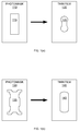
When the feature size of the integrated circuit were relatively large, lithography techniques could easily transfer the geometric pattern of the photomask to the thin film. However, due to advancement in other areas of semiconductor processing, optical constraints in lithography processes has become a limiting factor of the feature size of semiconductor devices. Advancement in lithography allows feature sizes to be smaller than the wavelength of light used in the lithography pattern. However, the geometric pattern of the photomask does not transfer cleanly to the thin film. For example, as illustrated in FIG. 1( a), a rectangle 115 in a photomask 110 may result in a peanut shape 125 on thin film 120. In general, lithography steppers are limited to a critical dimension CD that is equal to a process factor (K1) multiplied by the frequency of the light used by the stepper (λ) divided by the numerical aperture (NA) (as show in Equation EQ1).
CD=(K1*λ)/NA  (EQ1)
Lithography technology in 2007 uses deep ultraviolet light, which has a wavelength of 193 nm. The numerical aperture NA has a upper limit of 0.85 which can be increased using immersion technology to about 1.3-1.4. Because, the light frequency and numerical aperture are physically limited lithography processes attempt to reduce critical dimensions by reducing process factor k1 using various resolution enhancement techniques (RET) to improve the geometric pattern on the thin film. For example, in optical proximity correction(OPC), portions of the geometric pattern is reshaped to compensate for the deformity from the lithography process. As illustrated in FIG. 1( b), a reshaped polygon 135 (based on rectangle 115 of FIG. 1( a) with enhanced corners and sides) in a photomask 130 results in a near rectangular shape 145 on thin film 140. Near rectangular shape 145 approximates rectangle 115 more closely than peanut shape 125. Thus, RET/OPC can be used to improve the quality of the geometric pattern produced on the thin film and thus provides a better process factor K1.
However, RET/OPC require very complicated design rules. In addition, design rule technology in general can not adequately describe the complicated constraints of RET/OPC. Thus, even if a design passes the design rules, the integrated circuit manufactured from the design may still have “hot spots”, i.e. areas which would cause failure of the integrated circuit. Thus, excessive design rules are created for use with RET/OPC techniques to minimize the chances of hot spots in the fabricated devices. The excessive design rules are likely to lead to false violations, which would greatly increase the design time required for integrated circuits to address all the false violations.
Alternatively, hot spot detection and correction may be delayed until after RET/OPC. However, the post RET/OPC hot spot detection and correction would require detailed information about the RET/OPC process that is used by each foundry. Furthermore, each new generation of RET/OPC techniques may require years of development. Thus, IC development and design typically occurs long before the RET/OPC techniques are certified. In addition, simulation required to perform the post RET/OPC hot spot detection and correction is extremely time consuming and can greatly delay the IC design. Hence there is a need for a method and apparatus for rapidly detecting potential hot spots (sensitive spots) in an IC design.
SUMMARY
Accordingly, the present invention provides a fast method to detect sensitive spots using foundry independent models that do not require RET/OPC synthesis. For example, in some embodiments of the present invention, a plurality of sensitive spots are located. Lithography models are used to simulate the geometry near the sensitive spots to produce a model of the area around the sensitive spots. The sensitive spots are scored using a measure such as intensity (of light) or contrast.
Some embodiments of the present invention locate bridging sensitive spots others locate pinching sensitive spots and others locate both bridging and pinching sensitive spots.
Specifically, in some embodiment of the present invention the lithography model is a foundry independent model that uses critical dimension that is smaller than the actual critical dimension of the fabrication process that will be used. By using a smaller critical dimension, the lithography models of the present invention do not require resolution enhancement techniques or optical proximity correction.
The present invention will be more fully understood in view of the following description and drawings.
BRIEF DESCRIPTION OF THE FIGURES
FIGS. 1( a)-1(b) are a simplified diagrams of lithography used in IC manufacturing.
FIG. 2 is a simplified representation of an exemplary digital IC design flow in accordance with one embodiment of the present invention.
FIG. 3 is a flow chart of one embodiment of the present invention.
FIG. 4 illustrates a simplified design layout with sensitive spots in accordance with one embodiment of the present invention.
FIGS. 5( a)-5(c) illustrate scoring of bridging sensitive spots in accordance with some embodiments of the present invention.
FIGS. 6( a)-6(c) illustrate scoring of pinching sensitive spots in accordance with some embodiments of the present invention.
DETAILED DESCRIPTION
It may be helpful to place the processes of this invention in context of the overall chip design. FIG. 2 shows a simplified representation of an exemplary digital IC design flow. At a high level, the process starts with the product idea (200) and is realized in a EDA software design process (210). When the design is finalized, it can be taped-out (event 240). After tape out, the fabrication process (250) and packaging and assembly processes (260) occur resulting, ultimately, in finished chips (result 270).
The EDA software design process (210) is actually composed of a number of stages 212-230, shown in linear fashion for simplicity. In an actual IC design process, the particular design might have to go back through steps until certain tests are passed. Similarly, in any actual design process, these steps may occur in different orders and combinations. This description is therefore provided by way of context and general explanation rather than as a specific, or recommended, design flow for a particular IC. A brief description of the components of the EDA software design process (stage 210) will now be provided.
System design (stage 212): The circuit designers describe the functionality that they want to implement, they can perform what-if planning to refine functionality, check costs, etc. Hardware-software architecture partitioning can occur at this stage. Exemplary EDA software products from Synopsys, Inc. that can be used at this stage include Model Architect, Saber, System Studio, and DesignWare® products.
Logic design and functional verification (stage 214): At this stage, the VHDL or Verilog code for modules in the system is written and the design (which may be of mixed clock domains) is checked for functional accuracy. More specifically, the design is checked to ensure the design produces the correct outputs. Exemplary EDA software products from Synopsys, Inc. that can be used at this stage include VCS, VERA, DesignWare®, Magellan, Formality, ESP and LEDA products.
Synthesis and design for test (stage 216): Here, the VHDL/Verilog is translated to a netlist. The netlist can be optimized for the target technology. Additionally, the design and implementation of tests to permit checking of the finished chip occurs. Exemplary EDA software products from Synopsys, Inc. that can be used at this stage include Design Compiler®, Physical Compiler, Test Compiler, Power Compiler, FPGA Compiler, Tetramax, and DesignWare® products.
Design planning (stage 218): Here, an overall floorplan for the chip is constructed and analyzed for timing and top-level routing. Exemplary EDA software products from Synopsys, Inc. that can be used at this stage include Jupiter and Flooplan Compiler products. Although circuitry and portions thereof (such as standard cells) are described herein as if they exist in the real world, it is to be understood that at this stage only a computer model exists in a programmed computer. The actual circuitry in the real world is created after this stage.
Netlist verification (stage 220): At this step, the netlist is checked for compliance with timing constraints and for correspondence with the VHDL/Verilog source code. Exemplary EDA software products from Synopsys, Inc. that can be used at this stage include VCS, VERA, Formality and PrimeTime products.
Physical implementation (stage 222): The placement (positioning of circuit elements) and routing (connection of the same) occurs at this step. Exemplary EDA software products from Synopsys, Inc. that can be used at this stage include the Astro product.
Analysis and extraction (stage 224): At this step, the circuit function is verified at a transistor level, this in turn permits what-if refinement. Exemplary EDA software products from Synopsys, Inc. that can be used at this include Star RC/XT, Raphael, and Aurora products.
Physical verification (stage 226): At this stage various checking functions are performed to ensure correctness for: manufacturing, electrical issues, lithographic issues, and circuitry. Exemplary EDA software products from Synopsys, Inc. that can be used at this include the Hercules product. In accordance with the present invention, Lithography grading 219 as described in detail below, occurs during physical verification 226 and may require a return to physical implementation 222 to correct potential hot spots. Conventional systems may perform hot spot detection after resolution enhancement 228 (as explained above) or would require design rules tailored to the RET/OPC process for the specific foundry performing fabrication 250.
Resolution enhancement (stage 228): This stage involves geometric manipulations of the layout to improve manufacturability of the design. Exemplary EDA software products from Synopsys, Inc. that can be used at this include iN-Phase, Proteus, and AFGen products.
Mask data preparation (stage 230): This stage provides the “tape-out” data for production of masks for lithographic use to produce finished chips. Exemplary EDA software products from Synopsys, Inc. that can be used at this stage include the CATS(R) family of products.
FIG. 3 is a flow chart 300 illustrating an embodiment of the present invention for lithography printability grading in accordance with one embodiment of the present invention. First sensitive spots are located in LOCATE SENSITIVE SPOTS 310. Sensitive spots are areas of the design layout that are more likely to be actual hot spots after fabrication. Sensitive spot location is performed using user defined parameters for various types of potential problems such as bridging (short circuits) and pinching (open circuits). A primary benefit of the present invention is that the sensitive spots are detected automatically after the parameters are defined. Generally, sensitive spots for the same type of potential problem are processed together. Sensitive spot location in accordance with some embodiments of the present invention are described below. Each sensitive spot is individually analyzed and scored in APPLY LITHOGRAPHY MODEL 320 and CALCULATE SCORE 330. Specifically, a user defined area around each sensitive spot is simulated using lithography models for the geometries. In general a large area is simulated to better include other features that may cause problems near the sensitive spot. For example, in one embodiment of the present invention for a process using a wave length of 193 nm, a 1 micron radius area is used for the simulation. In another embodiment using a wavelength of 157 nm a 0.5 micron radius area is used for simulation. Foundry independent lithography models are used unless foundry specific models are available. The simulation of the area around the sensitive spot is analyzed and given a score that indicates the likelihood of the sensitive spot resulting in an actual hot spot during fabrication. Various novel scoring methods in accordance with embodiments of the present invention are described below.
In accordance with one embodiment of the present invention, the foundry independent lithography models are “next generation” lithography models without resolution enhancement techniques. Specifically, the foundry independent lithography models use values of light wavelength λ and numerical aperture NA that result in a smaller critical dimension CD than for the actual lithography process that is slated to be used in the fabrication of the design. Generally, the foundry independent lithography models use a smaller light wavelength λ, a higher numerical aperture NA, or a combination of smaller light wavelength λ and higher numerical aperture NA. For example, some embodiments of the present invention use light wavelength values of 157 nm or 120 nm instead of the 193 nm of the actual lithography process slated for fabrication. However, some embodiments of the present invention may use a much smaller light wavelength or with a much larger numerical aperture and still obtain a smaller critical dimension CD. (see equation EQ1). By using a “next generation” foundry independent lithography model, that does not include resolution enhancement techniques, the present invention approximates the results obtained with current lithography processes enhanced with resolution enhancement techniques. Because resolution enhancement techniques are not used in the foundry independent lithography model, the problems described above (i.e., excessive and often incomplete design rules and long simulation times) are greatly reduced.
In some embodiments of the present invention a novel light intensity tracing process is used in CALCULATE SCORE 330 for each sensitive spot. However, other embodiments of the present invention may use conventional methods to score the sensitive spots. After the sensitive spots are scored the sensitive spots are sorted and ranked based on the score in RANK SENSITIVE SPOTS 340. Generally, only sensitive spots for the same potential problems are grouped together for sorting and ranking. Thus, in one embodiment of the present invention separate rankings are made for bridging sensitive spots and pinching sensitive spots.
After ranking, sensitive layout patterns around sensitive spots (i.e. sensitive spots with scores indicating a likelihood of failure) are extracted in EXTRACT SENSITIVE LAYOUT PATTERNS 350. The factors determining whether a sensitive spot is a sensitive spot can be user defined and are generally based on the fabrication process and the scoring method. The sensitive layout patterns can be modified to avoid potential manufacturing problems.
Alternatively, the ranking of sensitive spots can be used to generate correction guidance GENERATE CORRECTION GUIDANCE 360. Guidance correction in general involves increasing the spacing between patterns for sensitive spots that may result in short circuits or increasing pattern size for sensitive spots that may result in open circuits. For example in a particular embodiment of the present invention, sizing changes are advised to be two grid points (For 65 nanometer process and 90 nanometer process grid points are usually 5 nanometers apart.) As used herein grid points are the manufacturing grid points used by the targeted process.
FIG. 4 illustrates potential sensitive spots for a simplified design layout 400 which is simulated using the “next generation” lithography models described above. Complicated features are divided into smaller rectangular features. For example, rectangular features 412, 414, and 416 are portions of an “I” shaped feature. Similarly, rectangular features 432 and 434 are part of a “T” shaped feature (rotated 90 degrees) and rectangular features 473 and 474 are portions of another “T” shaped feature. Design layout 400 also includes rectangular features 420, 440, 450, and 460. Rectangular features are used in the examples herein for clarity. However, the principles of the present invention are also applicable to more complicated shapes. In general the features of concern for sensitive spot (and hot spots) are conductors such as metals, heavily doped silicon, silicides, and salicides.
Sensitive spot location is performed using user defined parameters for various types of potential problems such as bridging (short circuits) and pinching (open circuits) problems. Bridging may occur if features in the design are too close together. For example in FIG. 4, a bridging sensitive spot 482 is located where rectangular features 412 and 432 are very close together and a second bridging sensitive spot 484 is located where rectangular features 432 and 460 are close together. In one embodiment of the present invention, a user defined bridging distance parameter defines the minimum distance between features that creates a bridging sensitive spot. Various geometric searching algorithms can be used to find features that separated by less than bridging distance parameter. For example, various EDA packages, such as ICC, Hercules or Calibre include searching algorithms that can be used to locate bridging sensitive spots.
To improve search speeds some embodiments of the present invention use a bridging search area around a current feature. For example, in a specific embodiment of the present invention, the bridging search area for the current feature is defined by a user defined bridging search distance from the perimeter of the feature. All other features within the bridging search area are compared with the current feature and sensitive spots are located wherever a feature is closer than the bridging distance parameter to the current feature. In a specific embodiment of the present invention for a fabrication process having minimum distance (separation distance) of 100 nm (for 65 nm technology Metal 2), the bridging search distance and bridging distance parameter is 120 nm. Other embodiments may use a smaller bridging distance parameter. In some embodiments of the present invention bridging search distance and bridging distance parameter are defined with grid points. Furthermore most embodiments of the present invention have default values for the user defined parameters. For example in a particular embodiment of the present invention the default bridging search distance is the minimum distance plus 4 grid points and the bridging distance parameter is the minimum distance plus 2 grid points.
Pinching may occur when a first feature is sandwiched between a second feature and a third feature. For example in FIG. 4, a pinching sensitive spot 486 is located where the portion of rectangular feature 414 is sandwiched between rectangular features 440 and 450. A second pinching sensitive spot 488 is located where the portion of rectangular feature 460 is sandwiched between rectangular feature 416 and 472. In one embodiment of the present invention, a user defined pinching distance parameter and a user defined pinching length parameters are used in the location of pinching sensitive spots. Specifically, the pinching distance parameter defines the minimum distance between the features of the “sandwich” to be considered a sensitive spot. The pinching length parameter defines the minimum length of the sandwich to be considered a sensitive spot. Conventional techniques, such as available in various EDA packages, such as ICC, Hercules or Calibre can be used to locate pinching sensitive spots. To reduce the search time, some embodiments of the presenting invention define a pinching search area for each feature. In one embodiment of the present invention the pinching search area for a current feature is defined by a pinching search distance extending from the perimeter of the current feature. All other features within the pinching search area are compared with the current feature and sensitive spots are located wherever a sandwich pattern having a first feature that is closer than the pinching distance parameter on one side of the current feature, a second feature that is closer than the pinching distance parameter on the opposite side of the current feature, and an overlap length that is greater than the pinching length parameter. In a specific embodiment of the present invention for a fabrication process having a critical dimension of 100 nm, the pinching search distance is 120 nm, the pinching distance parameter is also 120 nm, and the pinching length parameter is 100 nm. In some embodiments of the present invention pinching search distance and pinching distance parameter are defined with grid points. Furthermore most embodiments of the present invention have default values for the user defined parameters. For example in a particular embodiment of the present invention the default pinching search distance is the critical distance plus 4 grid points, the pinching distance parameter is the critical distance plus 2 grid points, the pinching length parameter is 100 nm.
As explained above, a large area around each sensitive spot is simulated using the lithography models. Generally the area simulated would include other rectangular features. For example the simulation area for sensitive spot 484 would likely include portions of rectangular features 416 and 472 and may even include portions of rectangular feature 450 and 474. Similarly, the simulation area for sensitive spot 488 would likely include portions rectangular features 414, 440, 450, 432, and 474. Scoring is then performed on the simulated area.
FIGS. 5( a)-5(b) illustrate scoring of bridging sensitive spots. Specifically, in FIG. 5( a) a rectangular feature 510 is close to a second rectangular feature 520, which is also close to a third rectangular feature 530. The key area of a first bridging sensitive spot is illustrated as a shaded area 540 and the key area of a second bridging sensitive spot is illustrated as a shaded area 550. The key area is limited by the portions of the features that actually overlap. Thus, for example in FIG. 5( a) key area 540 of the first bridging sensitive spot is limited by the upper and lower edges of rectangular feature 510 and key area 550 of the second bridging sensitive spot is limited by the top edge of rectangular feature 530 and the bottom edge of rectangular area 520.
Then as illustrated in FIG. 5( b), bridging scoring lines are defined through the middle of the key areas between the two features. The bridging scoring lines extend slightly beyond the border of the key area. The amount of extension can be a user defined parameter. Specifically, in FIG. 5( b) a bridging scoring line 545 is defined through the middle key area 540 with endpoints outside the borders of key area 545. Similarly a bridging scoring line 555 is defined through the middle of key area 550 with endpoints outside of key area 550. Scoring of the bridging sensitive spot is performed along the corresponding bridging scoring line.
In one embodiment of the present invention, scoring is based on light intensity along the bridging scoring line. Light intensity can be obtained using an aerial image simulator, which is included in many EDA software packages. Specifically, conducting regions (e.g. the rectangular features) are “light” regions while the non conducting regions are “dark” regions. For bridging sensitive spots higher light intensity indicates a greater chance of the bridging sensitive spot being shorted and thus a greater chance of the bridging sensitive spot being an actual hot spot during manufacturing. Thus the score for a key area is the highest light intensity on the scoring line. Generally, the score is normalized and any score above a user defined bridging threshold is considered a highly sensitive spot that should be redesigned. The user defined bridging threshold is generally in the range 0.15 to 0.3 for a 65 nm process using a 193 nm wavelength stepper using an alternating phase shift mask.
In another embodiment of the present invention, contrast comparisons are used for scoring. FIG. 5( c) is an enlarged view of key area 540, rectangular feature 520 and a portion of rectangular feature 510. As illustrated in FIG. 5( c), key area 540 encompasses a multitude of grid points GP. A bridging offset direction (vertical or horizontal) is defined for the key area. The offset direction is horizontal if the two features defining the key area are horizontally offset. For key area 540 the offset direction is horizontal. For the key area is sensitive spot 484 (FIG. 4) the offset direction would be vertical.
For each line of grid points in the offset direction (horizontal in key area 540) a line contrast score is computed. The line contrast score for a line of grid points is the difference between the maximum contrast at a grid point in the line and the minimum contrast at a grid point in the line divided by the sum of the maximum contrast at a grid point in the line and the minimum contrast at a grid point in the line. Equation EQ1 shows how to calculate the line contrast score LCS symbolically, where Cmax is the maximum contrast at a grid point in the line and Cmin is the minimum contrast at a grid point in the line.
LCS=(Cmax−Cmin)/(Cmax+Cmin)  EQ1
The bridging score for the key area is equal to the highest line contrast score of any line in the key area. Using this scoring technique, the lower the score the greater the possibility of bridging.
FIGS. 6( a)-6(b) illustrate scoring of pinching sensitive spots. Specifically, in FIG. 6( a) a rectangular feature 610 is sandwiched by rectangular features 610 and 630 and is also sandwiched by rectangular features 640 and 650. The key area of a first pinching sensitive spot is illustrated as a shaded area 670 and the key area of a second bridging sensitive spot is illustrated as a shaded area 670. The key area is limited by the portions of the features that actually overlap. Thus, for example in FIG. 6( a) key area 660 of the first pinching sensitive spot is limited by the left edge of rectangular feature 610 and the right edge of rectangular feature 630. Furthermore, for pinching sensitive spots, the ends of the center feature in the sandwich is not a major concern for open circuits; therefore, most embodiments of the present invention retract the edge of any key areas away from the ends of the center feature of a sandwich by a user defined pinching end retraction parameter (PERP in FIG. 6( a)). Thus, as illustrated in FIG. 6( a), key area 670 of the second pinching sensitive spot is limited by the left edge of rectangular feature 640 and the right edge of rectangular feature 620 retracted by the pinching end retraction parameter PERP.
Then as illustrated in FIG. 6( b), pinching scoring lines are defined through the middle of the center rectangular feature of the sandwich in parallel with the center rectangular feature. The scoring lines extend slightly beyond the border of the key area. The amount of extension can be a user defined parameter. Specifically, in FIG. 6( b) a pinching scoring line 665 is defined through the middle of rectangular feature 620 with endpoints outside the borders of key area 660. Similarly a pinching scoring line 575 is defined through the middle of rectangular feature 620 with endpoints outside of key area 670. Scoring of the pinching sensitive spot is performed along the corresponding pinching scoring line.
In one embodiment of the present invention, scoring is based on light intensity along the pinching scoring line. Specifically, conducting regions (e.g. the rectangular features) are “light” regions while the non conducting regions are “dark” regions. For pinching sensitive spots lower light intensity indicates a greater chance of the sensitive spot being shorted and thus a greater chance of the sensitive spot being an actual hot spot. To reverse this relationship many embodiments of the present invention normalize the intensity values and then use 1 minus the normalized intensity value as the score for pinching sensitive spots. Any score above a user defined pinching threshold is considered a highly sensitive spot that should be redesigned. The user defined pinching threshold is generally in the range 0.15 to 0.3.
In another embodiment of the present invention, contrast comparisons are used for scoring. FIG. 6( c) is an enlarged view of key area 660, rectangular feature 610, rectangular feature 630 and a portion of rectangular feature 620. As illustrated in FIG. 6( c), key area 660 encompasses a multitude of grid points GP. An offset direction (vertical or horizontal) is defined for the key area direction (vertical or horizontal) is defined for the key area. The bridging offset direction is orthogonal to the direction of the sandwich of features defining the key. Thus for key area 660 the pinching offset direction is vertical. For the key area is sensitive spot 486 (FIG. 4) the pinching offset direction would be horizontal. The offset direction is vertical if the three features defining the key area are vertically offset from each other.
For each line of grid points in the pinching offset direction (vertical in key area 660) a line contrast score is computed. The line contrast score for a line of grid points is the difference between the maximum contrast at a grid point in the line and the minimum contrast at a grid point in the line divided by the sum of the maximum contrast at a grid point in the line and the minimum contrast at a grid point in the line. Equation EQ1 given above shows how to calculate the line contrast score LCS symbolically, where Cmax is the maximum contrast at a grid point in the line and Cmin is the minimum contrast at a grid point in the line.
The pinching score for the key area is equal to the lowest line contrast score of any line in the key area. Using this scoring technique, the lower the score the greater the possibility of pinching.
After the sensitive spots of a particular category (e.g. the pinching sensitive spots and the bridging sensitive spots) are scored. The sensitive spots can be ranked to generate a chip health graph. The chip health graph gives a fast summary regarding the “health of the chip” with respect to bridging and pinching.
Thus lithography printability grading for sensitive spots in accordance with the present invention make use of “next generation” lithography models without resolution enhancement techniques to approximate the results of current generation lithography processes using resolution enhancement techniques. Thus the present invention avoids the complication and difficulties of simulating the resolution enhancement techniques.
Generally, the present invention is likely to be implemented on a computer as part of an EDA package. The computer programmed in accordance with the invention receives a design of an integrated circuit device. Then, with appropriate parameters from the user, the locations of the sensitive spots are located and evaluated as described above.
The data structures and software code for implementing one or more acts described in this detailed description can be stored on a computer readable storage medium, which may be any device or medium that can store code and/or data for use by a computer system. This includes, but is not limited to, magnetic and optical storage devices such as disk drives, magnetic tape, CDs (compact discs) and DVDs (digital versatile discs or digital video discs), and computer instruction signals embodied in a transmission medium (with or without a carrier wave upon which the signals are modulated). For example, the transmission medium may include a communications network, such as the Internet. In one embodiment, the carrier wave includes computer instruction signals for carrying out the process described above.
Numerous modifications and adaptations of the embodiments described herein will become apparent to the skilled artisan in view of this disclosure and are encompassed by the scope of the invention.

Claims (33)

1. A method of identifying hot spots in an integrated circuit (IC) design for use with a fabrication process having a first critical dimension, the method comprising:
locating a plurality of sensitive spots in the IC design; and
simulating a plurality of areas around the sensitive spots using a plurality of lithography models having a second critical dimension by a computer processor, wherein the second critical dimension is smaller than the first critical dimension of the fabrication process.
2. The method of claim 1, wherein the locating a plurality of sensitive spots in the IC design comprises locating a plurality of bridging hot spots.
3. The method of claim 2, wherein the locating a plurality of bridging hot spots comprises: finding a first feature of the IC design within a bridging distance from a second feature IC design.
4. The method of claim 1, wherein the locating a plurality of sensitive spots in the IC design comprises locating a plurality of pinching hot spots.
5. The method of claim 4, wherein the locating a plurality of pinching hot spots comprises finding a first feature sandwiched between a second feature and a third feature, wherein the second feature and the third feature are within a pinching distance from the first feature.
6. The method of claim 1, wherein the lithography models use a smaller light wavelength than the fabrication process.
7. The method of claim 1, wherein the lithography models use a higher numerical aperture than the fabrication process.
8. The method of claim 1, wherein the fabrication process includes using resolution enhancement techniques and the simulating a plurality of areas around the sensitive spots does not include using resolution enhancement techniques.
9. The method of claim 1, wherein the fabrication process includes using optical proximity correction and the simulating a plurality of areas around the sensitive spots does not comprise using optical proximity correction.
10. The method of claim 1, further comprising defining a key area within a sensitive spot.
11. The method of claim 10, further comprising scoring the key area.
12. The method of claim 11, wherein the scoring the key area comprises:
defining a scoring line within the key area; and
measuring light intensity along the scoring line based on a aerial image simulation.
13. The method of claim 12, wherein a highest light intensity is used to calculate the score for the key area.
14. The method of claim 12, wherein the lowest light intensity is used to calculate the score for the key area.
15. The method of claim 11, wherein the scoring the key area comprises calculating a line contrast score for a plurality of lines in the key area.
16. The method of claim 11, wherein the scoring the key are comprises:
defining an offset direction; and
calculating a line contrast score for a plurality of lines of grid points within the key area; where the lines are in the offset direction.
17. The method of claim 16, wherein the lowest line contrast score is used to calculate the score for the key area.
18. The method of claim 1, wherein the lithography models are foundry independent.
19. The method of claim 1, wherein a size of the plurality of areas is user-definable.
20. A computer storage device encoded with instructions to perform the method of claim 1.
21. A computer system configured to identify hot spots in an integrated circuit (IC) design for use with a fabrication process having a first critical dimension by:
locating a plurality of sensitive spots in the IC design; and
simulating a plurality of areas around the sensitive spots using a plurality of lithography models having a second critical dimension, wherein the second critical dimension is smaller than the first critical dimension of the fabrication process.
22. A computer system for identifying hot spots in an integrated circuit (IC) design for use with a fabrication process having a first critical dimension, the computer system comprising:
means for locating a plurality of sensitive spots in the IC design; and
means for simulating a plurality of areas around the sensitive spots using a plurality of lithography models having a second critical dimension, wherein the second critical dimension is smaller than the first critical dimension of the fabrication process.
23. The computer system of claim 22, wherein the means for locating a plurality of sensitive spots in the IC design comprises means for locating a plurality of bridging hot spots.
24. The computer system of claim 22, wherein the means for locating a plurality of sensitive spots in the IC design comprises means for locating a plurality of pinching hot spots.
25. The computer system of claim 22, wherein the lithography models use a smaller light wavelength than the fabrication process.
26. The computer system of claim 22, wherein the lithography models use a higher numerical aperture than the fabrication process.
27. The computer system of claim 22, wherein the fabrication process includes using resolution enhancement techniques and the means for simulating a plurality of areas around the sensitive spots does not include using resolution enhancement techniques.
28. The computer system of claim 22, wherein the fabrication process includes using optical proximity correction and the means for simulating a plurality of areas around the sensitive spots does not comprise using optical proximity correction.
29. The computer system of claim 22, further comprising means for defining a key area within a sensitive spot.
30. The computer system of claim 22, further comprising means for scoring the key area.
31. The computer system of claim 30, wherein the scoring the key area comprises:
means for defining a scoring line within the key area; and
means for measuring light intensity along the scoring line based on a aerial image simulation.
32. The computer system of claim 30, wherein the scoring the key area comprises means for calculating a line contrast score for a plurality of lines in the key area.
33. The computer system of claim 32, wherein the means for scoring the key are comprises:
means for defining an offset direction; and
means for calculating a line contrast score for a plurality of lines of grid points within the key area; where the lines are in the offset direction.
US11/756,596 2007-05-31 2007-05-31 Lithography suspect spot location and scoring system Active 2028-08-07 US7823099B2 (en)

Priority Applications (1)

Application Number Priority Date Filing Date Title
US11/756,596 US7823099B2 (en) 2007-05-31 2007-05-31 Lithography suspect spot location and scoring system

Applications Claiming Priority (1)

Application Number Priority Date Filing Date Title
US11/756,596 US7823099B2 (en) 2007-05-31 2007-05-31 Lithography suspect spot location and scoring system

Publications (2)

Publication Number Publication Date
US20080301623A1 US20080301623A1 (en) 2008-12-04
US7823099B2 true US7823099B2 (en) 2010-10-26

Family

ID=40089725

Family Applications (1)

Application Number Title Priority Date Filing Date
US11/756,596 Active 2028-08-07 US7823099B2 (en) 2007-05-31 2007-05-31 Lithography suspect spot location and scoring system

Country Status (1)

Country Link
US (1) US7823099B2 (en)

Cited By (6)

* Cited by examiner, † Cited by third party
Publication number Priority date Publication date Assignee Title
US20100023905A1 (en) * 2008-02-20 2010-01-28 Pikus Fedor G Critical Area Deterministic Sampling
US20100180247A1 (en) * 2005-05-20 2010-07-15 Scheffer Louis K Aware manufacturing of integrated circuits
US20110314436A1 (en) * 2005-05-20 2011-12-22 Akira Fujimura Aware manufacturing of an integrated circuit
US8453075B2 (en) 2011-09-02 2013-05-28 International Business Machines Corporation Automated lithographic hot spot detection employing unsupervised topological image categorization
US8732629B2 (en) 2009-10-30 2014-05-20 Synopsys, Inc. Method and system for lithography hotspot correction of a post-route layout
US20140358830A1 (en) * 2013-05-30 2014-12-04 Synopsys, Inc. Lithographic hotspot detection using multiple machine learning kernels

Families Citing this family (7)

* Cited by examiner, † Cited by third party
Publication number Priority date Publication date Assignee Title
US8650511B2 (en) 2010-04-30 2014-02-11 Taiwan Semiconductor Manufacturing Company, Ltd. Lithography performance check methods and apparatus
DE102010030758B4 (en) * 2010-06-30 2018-07-19 Globalfoundries Dresden Module One Limited Liability Company & Co. Kg Control critical dimensions in optical imaging processes for semiconductor fabrication by extracting aberrations based on imaging plant-specific intensity measurements and simulations
US8898600B2 (en) * 2013-03-15 2014-11-25 Taiwan Semiconductor Manufacturing Company, Ltd. Layout optimization for integrated design
US9418196B2 (en) 2013-03-15 2016-08-16 Taiwan Semiconductor Manufacturing Company, Ltd. Layout optimization for integrated circuit design
US8997027B2 (en) * 2013-07-31 2015-03-31 GlobalFoundries, Inc. Methods for modifying an integrated circuit layout design
US9171127B1 (en) * 2014-10-08 2015-10-27 United Microelectronics Corp. Layout generating method
CN108009316B (en) * 2017-11-09 2021-08-13 上海华力微电子有限公司 OPC correction method

Citations (5)

* Cited by examiner, † Cited by third party
Publication number Priority date Publication date Assignee Title
US20050132322A1 (en) * 2003-10-31 2005-06-16 Mari Inoue Mask evaluating method, mask evaluating system, method of manufacturing mask and computer program product
US20070044049A1 (en) * 2005-08-18 2007-02-22 International Business Machines Corporation Apparatus and methods for predicting and/or calibrating memory yields
US20070266362A1 (en) * 2006-05-15 2007-11-15 Taiwan Semiconductor Manufacturing Company, Ltd. Method for Detection and Scoring of Hot Spots in a Design Layout
US7448012B1 (en) * 2004-04-21 2008-11-04 Qi-De Qian Methods and system for improving integrated circuit layout
US20080295046A1 (en) * 2007-05-25 2008-11-27 Qing Su Predicting IC manufacturing yield based on hotspots

Patent Citations (5)

* Cited by examiner, † Cited by third party
Publication number Priority date Publication date Assignee Title
US20050132322A1 (en) * 2003-10-31 2005-06-16 Mari Inoue Mask evaluating method, mask evaluating system, method of manufacturing mask and computer program product
US7448012B1 (en) * 2004-04-21 2008-11-04 Qi-De Qian Methods and system for improving integrated circuit layout
US20070044049A1 (en) * 2005-08-18 2007-02-22 International Business Machines Corporation Apparatus and methods for predicting and/or calibrating memory yields
US20070266362A1 (en) * 2006-05-15 2007-11-15 Taiwan Semiconductor Manufacturing Company, Ltd. Method for Detection and Scoring of Hot Spots in a Design Layout
US20080295046A1 (en) * 2007-05-25 2008-11-27 Qing Su Predicting IC manufacturing yield based on hotspots

Cited By (9)

* Cited by examiner, † Cited by third party
Publication number Priority date Publication date Assignee Title
US20100180247A1 (en) * 2005-05-20 2010-07-15 Scheffer Louis K Aware manufacturing of integrated circuits
US20110314436A1 (en) * 2005-05-20 2011-12-22 Akira Fujimura Aware manufacturing of an integrated circuit
US8302061B2 (en) * 2005-05-20 2012-10-30 Cadence Design Systems, Inc. Aware manufacturing of an integrated circuit
US8713484B2 (en) 2005-05-20 2014-04-29 Cadence Design Systems, Inc. Aware manufacturing of integrated circuits
US20100023905A1 (en) * 2008-02-20 2010-01-28 Pikus Fedor G Critical Area Deterministic Sampling
US8732629B2 (en) 2009-10-30 2014-05-20 Synopsys, Inc. Method and system for lithography hotspot correction of a post-route layout
US8453075B2 (en) 2011-09-02 2013-05-28 International Business Machines Corporation Automated lithographic hot spot detection employing unsupervised topological image categorization
US20140358830A1 (en) * 2013-05-30 2014-12-04 Synopsys, Inc. Lithographic hotspot detection using multiple machine learning kernels
US11403564B2 (en) 2013-05-30 2022-08-02 Synopsys, Inc. Lithographic hotspot detection using multiple machine learning kernels

Also Published As

Publication number Publication date
US20080301623A1 (en) 2008-12-04

Similar Documents

Publication Publication Date Title
US7823099B2 (en) Lithography suspect spot location and scoring system
US20210073455A1 (en) Integrated circuits having in-situ constraints
US8612899B2 (en) Fast lithography compliance check for place and route optimization
US7934174B2 (en) Method and apparatus for using a database to quickly identify and correct a manufacturing problem area in a layout
US8037428B2 (en) Method and system for post-routing lithography-hotspot correction of a layout
US8578313B2 (en) Pattern-clip-based hotspot database system for layout verification
US8132128B2 (en) Method and system for performing lithography verification for a double-patterning process
CN102768696B (en) Incremental analysis of layout design data
US7191428B2 (en) Centerline-based pinch/bridge detection
US8566754B2 (en) Dual-purpose perturbation engine for automatically processing pattern-clip-based manufacturing hotspots
US11003828B1 (en) System and method for layout analysis using point of interest patterns and properties
US20100257496A1 (en) Design-Rule-Check Waiver
Roseboom et al. Automated full-chip hotspot detection and removal flow for interconnect layers of cell-based designs
US10089432B2 (en) Rule-check waiver
US20130263074A1 (en) Analog Rule Check Waiver
US20100138019A1 (en) Method of performing optical proximity effect corrections to photomask pattern
US20110265054A1 (en) Design-Rule-Check Waiver
US20230053711A1 (en) Integrated circuit device design method and system
Mirsaeedi EDA Solutions for Double Patterning Lithography
Kagalwalla Computational Methods for Design-Assisted Mask Flows
Qian DFM through correct process construction
Wuu Design Methodologies for Optical Lithography Induced Systematic Variations
Lin et al. Silicon-verified automatic DFM layout optimization: a calibration-lite model-based application to standard cells
Park et al. Accurate Systematic Hot-Spot Scoring Method and Score-Based Fixing Guidance Generation

Legal Events

Date Code Title Description
AS Assignment

Owner name: SYNOPSYS, INC., CALIFORNIA

Free format text: ASSIGNMENT OF ASSIGNORS INTEREST;ASSIGNORS:TSAI, MIN-CHUN, MR.;CHIANG, CHARLES C., MR.;REEL/FRAME:019364/0406

Effective date: 20070525

STCF Information on status: patent grant

Free format text: PATENTED CASE

FPAY Fee payment

Year of fee payment: 4

MAFP Maintenance fee payment

Free format text: PAYMENT OF MAINTENANCE FEE, 8TH YEAR, LARGE ENTITY (ORIGINAL EVENT CODE: M1552)

Year of fee payment: 8

MAFP Maintenance fee payment

Free format text: PAYMENT OF MAINTENANCE FEE, 12TH YEAR, LARGE ENTITY (ORIGINAL EVENT CODE: M1553); ENTITY STATUS OF PATENT OWNER: LARGE ENTITY

Year of fee payment: 12