US7821334B2 - Amplification circuit - Google Patents
Amplification circuit Download PDFInfo
- Publication number
- US7821334B2 US7821334B2 US12/298,185 US29818507A US7821334B2 US 7821334 B2 US7821334 B2 US 7821334B2 US 29818507 A US29818507 A US 29818507A US 7821334 B2 US7821334 B2 US 7821334B2
- Authority
- US
- United States
- Prior art keywords
- signal
- circuit
- type
- switching circuit
- input
- Prior art date
- Legal status (The legal status is an assumption and is not a legal conclusion. Google has not performed a legal analysis and makes no representation as to the accuracy of the status listed.)
- Active, expires
Links
Images


Classifications
-
- H—ELECTRICITY
- H03—ELECTRONIC CIRCUITRY
- H03F—AMPLIFIERS
- H03F1/00—Details of amplifiers with only discharge tubes, only semiconductor devices or only unspecified devices as amplifying elements
- H03F1/56—Modifications of input or output impedances, not otherwise provided for
- H03F1/565—Modifications of input or output impedances, not otherwise provided for using inductive elements
-
- H—ELECTRICITY
- H03—ELECTRONIC CIRCUITRY
- H03F—AMPLIFIERS
- H03F1/00—Details of amplifiers with only discharge tubes, only semiconductor devices or only unspecified devices as amplifying elements
- H03F1/42—Modifications of amplifiers to extend the bandwidth
-
- H—ELECTRICITY
- H03—ELECTRONIC CIRCUITRY
- H03F—AMPLIFIERS
- H03F3/00—Amplifiers with only discharge tubes or only semiconductor devices as amplifying elements
- H03F3/005—Amplifiers with only discharge tubes or only semiconductor devices as amplifying elements using switched capacitors, e.g. dynamic amplifiers; using switched capacitors as resistors in differential amplifiers
-
- H—ELECTRICITY
- H03—ELECTRONIC CIRCUITRY
- H03F—AMPLIFIERS
- H03F3/00—Amplifiers with only discharge tubes or only semiconductor devices as amplifying elements
- H03F3/189—High-frequency amplifiers, e.g. radio frequency amplifiers
- H03F3/19—High-frequency amplifiers, e.g. radio frequency amplifiers with semiconductor devices only
- H03F3/195—High-frequency amplifiers, e.g. radio frequency amplifiers with semiconductor devices only in integrated circuits
-
- H—ELECTRICITY
- H03—ELECTRONIC CIRCUITRY
- H03F—AMPLIFIERS
- H03F3/00—Amplifiers with only discharge tubes or only semiconductor devices as amplifying elements
- H03F3/68—Combinations of amplifiers, e.g. multi-channel amplifiers for stereophonics
Definitions
- the present invention relates to an amplifier which has a wide dynamic range when it operates under a low voltage and which operates in a wide frequency range.
- GSM Global System for Mobile Communications
- DCS Digital Cellular system
- EDGE Enhanced Data GSM Environment
- CDMA Code Division Multiple Access
- WCDMA Wideband CDMA
- the frequency bands can be covered by a single circuit if its gain in desired frequency bands is sacrificed. Generally, however, a plurality of bands are available and selectively used to cover a wide frequency range (see, for example, Non-patent document 1).
- Non-patent document 1 discloses a multiband-compatible chip having a plurality of parallel-connected amplifiers having matching circuits for respective frequencies to cover a plurality of frequency bands. Each of the circuits corresponding to a desired frequency band is activated one at a time, with the other circuits being kept in a shut-off state.
- Another example which handles a plurality of frequency bands is a system proposed for suppressing input signals that will not be used by means of filters (see, for example, Patent document 1).
- Patent document 1 relates to a television receiver and comprises a wideband receiving circuit for receiving all terrestrial broadcasts and CATV channels.
- FIG. 1 is a circuit diagram of a band switching circuit proposed in Patent document 1.
- Filter FL 1 for passing a signal in a first frequency band and filter FL 2 for passing a signal in a second frequency band are connected in series to each other.
- Filter FL 1 is a high-pass filter comprising capacitors C 21 , C 22 , C 23 and inductors L 21 , L 22 for passing a signal in a low frequency range (e.g., 90 MHz and higher).
- Filter FL 2 is a high-pass filter comprising capacitors C 24 , C 25 , C 26 and inductor L 23 for passing a signal in a high frequency range (e.g., 470 MHz and higher).
- Switch device (PIN diode) SW 1 is connected parallel to second filter FL 2 . When filter FL 2 is required, switch 3 is turned off. When filter FL 2 is not required, switch 3 is turned on.
- Filter FL 2 includes switch device (PIN diode) SW 2 for turning on and off a series-connected resonant circuit of capacitor C 25 and inductor L 23 .
- switch SW 2 is turned off to disconnect the series-connected resonant circuit.
- switch device SW 1 When the band switching circuit is to receive a signal in a frequency band ranging from 90 to 470 MHz which is input from input terminal IN, switch device SW 1 is turned on and switch device SW 2 is turned off to put only filter FL 1 in operation while keeping filter FL 2 out of operation, thereby outputting the signal from output terminal OUT while bypassing filter FL 2 . Therefore, only a signal of 90 MHz or higher from filter FL 1 is output from output terminal OUT to an external circuit.
- switch device SW 1 When the band switching circuit is to receive a signal in a frequency band ranging from 470 MHz to 770 MHz, switch device SW 1 is turned off and switch device SW 2 is turned on to put filter FL 1 and filter FL 2 simultaneously in operation. Therefore, a signal of 90 MHz or higher that has passed through filter FL 1 is processed by filter FL 2 into a signal of 470 MHz or higher, which is output from output terminal OUT to the external circuit.
- Quadrature Amplitude Modulation QAM
- orthogonal frequency modulation OFDM
- the dynamic range may be considered to be from the maximum signal level that can be handled, to less a lower noise level.
- a circuit scheme for varying the gain of an amplifying circuit depending on the intensity of an input signal is employed to keep a wide dynamic range (see, for example, Patent document 2).
- FIG. 2 is a circuit diagram of a variable-gain amplifying circuit disclosed in Patent document 2.
- Gain control amplifying circuit 201 comprises amplifying transistor unit 202 and variable attenuators 203 a , 203 b disposed in a front stage thereof.
- Amplifying transistor unit 202 includes amplifying MOSFETs Q 30 , Q 31 and amplifying MOSFETs Q 32 , Q 33 that are connected parallel thereto.
- Differential input signals F 2 a , F 2 b that are input to input terminals INa, INb are supplied through respective variable attenuators 203 a , 203 b to the gates of amplifying MOSFETs Q 30 , Q 32 .
- First bias voltage Vbias 1 is supplied through resistor R 11 to the gates of amplifying MOSFETs Q 31 , Q 33 , and second bias voltage Vbias 2 is supplied through resistor R 12 to the gates of amplifying MOSFETs Q 30 , Q 32 .
- MOSFETs Q 31 , A 33 have respective drains connected to power supply terminal Vdd through load inductors L 31 , L 32 .
- the drains of MOSFETs Q 31 , A 33 output differential output signals Fouta, Foutb from output terminals OUTa, OUTb through output coupling capacitors Couta, Coutb.
- the overall gain of gain control amplifying circuit 201 is controlled by varying the attenuations of variable attenuators 203 a , 203 b which are connected between the gates of amplifying MOSFETs Q 30 , Q 32 of amplifying transistor unit 202 and input terminals INa, INb.
- Each of variable attenuators 203 a , 203 b includes input coupling capacitor Cin whose capacitance is variable and which is connected between input terminal INa (INb) and signal propagation path SPR leading to the gate of MOSFET Q 32 (Q 30 ).
- Input coupling capacitor Cin comprises a plurality of capacitors C 51 through C 54 and n-channel switching MOSFETs Q 51 through Q 54 .
- the capacitance of input coupling capacitor Cin is varied when these MOSFETs are rendered conductive and nonconductive by coupling capacitance control signals GC 11 through CG 14 .
- Signal propagation path SPR is connected to power supply ground by a plurality of (four in FIG. 2 ) parallel attenuating units comprising respective attenuating capacitors C 41 through C 44 and switching MOSFETs Q 41 through Q 44 connected in series thereto.
- Switching MOSFETs Q 41 through Q 44 have respective gates supplied with respective attenuation control signals GC 1 through CG 4 for rendering switching MOSFETs Q 41 through Q 44 conductive and nonconductive.
- High-frequency input signal F 2 a (F 2 b ) applied to input terminal INa (INb) is supplied through input coupling capacitor Cin and signal propagation path SPR to the gate of amplifying MOSFET Q 32 (Q 30 ).
- Attenuation control signal GC 1 reaches a high level to render MOSFET Q 41 conductive, then part of the energy of the high-frequency signal that is propagated through signal propagation path SPR is absorbed through attenuating capacitor C 41 and MOSFET Q 41 into ground.
- Attenuating capacitor C 41 has a function to short an AC component of the high-frequency signal to ground GND. The amount of energy that is absorbed is determined depending on the capacitance value of attenuating capacitor C 41 .
- variable attenuators are designed to increase the capacitance values of attenuating capacitors C 41 through C 44 in a binary fashion of 1:2:4:8, for example, and also if the widths of the gates of switching MOSFETs Q 41 through Q 44 are of the same ratio, then the attenuation of variable attenuator 203 a ( 203 b ) can be increased linearly by using attenuation control signals GC 1 through CG 4 in appropriate combinations.
- the attenuation is of the lowest level when all MOSFETs Q 41 through Q 44 are rendered nonconductive, and is linearly increased when MOSFETs Q 41 through Q 44 are rendered nonconductive in combinations.
- the amplitude of the input high-frequency input signal is linearly varied by attenuator 203 a ( 203 b ), and then amplified at a fixed gain by amplifying transistor unit 202 .
- the gain of the overall amplifying circuit is linearly varied. Since the gain is increased by two cascaded MOSFETs Q 30 , Q 31 of amplifying transistor unit 202 , the variable range of the gain can be widened.
- FIG. 3 shows a charge pump circuit as disclosed in Patent document 3 for boosting the control signals for signal switching circuits Q 51 through Q 54 shown in FIG. 2 .
- the charge pump circuit stores electric charges in capacitive elements using a clock for thereby obtaining a potential higher than an input potential.
- the charge pump circuit comprises a plurality of boosting stages for higher boosting efficiency.
- the boosting circuit comprises n boosting stages CP 1 , CP 2 , . . . CP n .
- Each boosting stage CP k (k is 1, 2, . . . , n) comprises first charge pump 11 and second charge pump 13 .
- First charge pump 11 of boosting stage CP k comprises n-type MOSFET nQ 1 k , p-type MOSFET pQ 1 k , and pumping capacitor C 1 k .
- Second charge pump 13 of boosting stage CP k comprises n-type MOSFET nQ 2 k , p-type MOSFET pQ 2 k , and pumping capacitor C 2 k .
- n-type MOSFET nQ 2 k and p-type MOSFET pQ 1 k are rendered conductive, charging capacitor C 2 k to the potential of node ND k-1 .
- the potential of the drain of p-type MOSFET pQ 1 k (the potential boosted by the clock provided by the charged potential of capacitor C 1 k ) is transferred to node ND k .
- n-type MOSFET nQ 1 k and p-type MOSFET pQ 2 k are rendered conductive, charging capacitor C 1 k to the potential of node ND k-1 .
- the potential of the drain of p-type MOSFET pQ 2 k (the potential boosted by the clock provided by the charged potential of capacitor C 2 k ) is transferred to node ND k .
- Non-patent document 1 2005 IEEE International Solid State Circuit Conference, SESSION 5, pp. 98-99 & 586
- Patent document 1 JP-U No. 5-48440
- Patent document 2 JP-A No. 2005-159803
- Patent document 3 JP-A No. 2000-69745
- the circuit scheme which has parallel circuits corresponding to respective frequencies for covering a plurality of frequency bands, as disclosed in Non-patent document 1, suffers a large cost problem because the chip size increases greatly as the number of compatible frequencies increases.
- Chips that are compatible with the advanced modulation system have been part of trends to reduce device sizes to meet requirements for higher baseband signal processing rates, and smaller device sizes have resulted in lower power supply voltages for processing baseband signals.
- SoC system-on-chip
- a filter circuit for suppressing a frequency other than a desired frequency is replaced with a matching circuit, then matching is possible at a plurality of frequencies.
- achieving a dynamic range requires an amplifying stage whose amplification factor can be varied greatly.
- Such an amplifying stage comprises cascaded transistors as shown in FIG. 2 , for example, with the result that the power supply voltage of the amplifying state cannot be lowered.
- Scaled MOS devices suffer a serious problem caused by standby power due to leakage current that flows even when the gate voltage is biased to a level equal to or lower than the threshold voltage.
- the present invention is aimed at solving the above problems of the background art. It is an object of the present invention to provide an amplifying circuit which has a wide dynamic range when it operates under a low voltage and which operates in a wide frequency range.
- an amplifying circuit comprising a plurality of impedance converting circuits connected to each other by a switching circuit of a first type having a signal cutting-off function, a switching circuit of a second type connected to a path branched from an input side of the switching circuit of the first type, the switching circuit of the second type having a signal cutting-off function, amplifiers connected respectively to an output side of one of the impedance converting circuits in a final stage and an output side of the switching circuit of the second type, and a control signal generating circuit for controlling connection/disconnection between said switching circuit of the first type and said switching circuit of the second type, wherein either one of the paths is selected to input a signal to one of the amplifiers.
- an amplifying circuit comprising a plurality of impedance converting circuits connected to each other along a path by a switching circuit of a first type having a signal cutting-off function, a switching circuit of a second type connected between an output side of the switching circuit of the first type and an input terminal which is different from an input terminal to which an input side of one of the impedance converting circuits in a first stage is connected, the switching circuit of the second type having a signal cutting-off function, an amplifier connected to an output side of one of the impedance converting circuits in a final stage, and a control signal generating circuit for controlling connection/cutting-off of the switching circuit of the first type and the switching circuit of the second type, wherein either one of the paths is selected to input a signal to one of the amplifiers.
- one or more switching circuits of the first type and the switching circuit of the second type has/have a signal attenuating function.
- the switching circuit having the signal cutting-off function and the signal attenuating function comprises a plurality of parallel-connected devices each controllable by the control signal generating circuit.
- the switching circuits which comprise MOS field-effect transistors have a substrate potential linked to a DC input voltage of the amplifier.
- a control potential is increased by a potential corresponding to the DC input voltage of the amplifier, using a clock signal applied from an external source.
- the impedance converting circuits are connected to each other by the switching circuit of the first type having the signal cutting-off function, and the switching circuit of the second type is connected to the signal path branched from the input side of the switching circuit of the first type, or the impedance converting circuits that are connected to each other by the switching circuit of the first type that have the signal cutting-off function are connected to the switching circuit of the second type that have the signal cutting-off function which is connected between the output and input sides of the switching circuit of the first type.
- the amplifying circuit is operable in a wide frequency band.
- the amplifying circuit Since the switching circuits connected in series to the amplifiers have the signal attenuating function, the amplifying circuit provide a wide dynamic range when it is operated under a low voltage.
- the amplifying circuit according to the present invention does not have a plurality of switch devices for connecting attenuating capacitors to and disconnecting attenuating capacitors from signal paths, the amplifying circuit can avoid leakage due to such switch devices, and can maintain good signal quality even when it is supplied with a weak signal input thereto.
- the switching circuits which comprise MOS field-effect transistors have the substrate potential linked to the DC input voltage of the amplifier, and since the control potential is increased by the potential corresponding to the DC input voltage of the amplifier, by using the clock signal applied from the external source, the on-resistances of the MOS field-effect transistors as the switching circuit are minimized, and a voltage in excess of a withstand voltage is prevented from being applied thereto.
- an amplifying circuit which is applicable to a software wireless terminal that is expected to be realized in the future.
- FIG. 1 is a circuit diagram of the background art disclosed in Patent document 1;
- FIG. 2 is a circuit diagram of the background art disclosed in Patent document 2;
- FIG. 3 is a circuit diagram of the background art disclosed in Patent document 3;
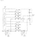
- FIG. 4 is a circuit diagram of a first exemplary embodiment of the present invention.
- FIG. 5 is a circuit diagram of a second exemplary embodiment of the present invention.
- FIG. 6 is a circuit diagram showing an example of an output matching circuit of an amplifying circuit according to the present invention.
- FIG. 7 is a circuit diagram of a third exemplary embodiment of the present invention.
- FIG. 8 is a circuit diagram of a fourth exemplary embodiment of the present invention.
- FIG. 9 is a circuit diagram of a fifth exemplary embodiment of the present invention.
- FIG. 10 is a circuit diagram of a sixth exemplary embodiment of the present invention.
- FIG. 11 is a circuit diagram of a seventh exemplary embodiment of the present invention.
- FIG. 12 is a circuit diagram of an eighth exemplary embodiment of the present invention.
- FIG. 13 is a circuit diagram of a ninth exemplary embodiment of the present invention.
- FIG. 14 is a circuit diagram of a tenth exemplary embodiment of the present invention.
- FIG. 15 is a circuit diagram illustrating a signal attenuating effect of a switching device (MOSFET) according to the present invention.
- FIG. 16 is a circuit diagram of an eleventh exemplary embodiment of the present invention.
- FIG. 17 is a circuit diagram showing an example of a boosting circuit used in the eleventh exemplary embodiment of the present invention.
- FIG. 18 is a circuit diagram of a twelfth exemplary embodiment of the present invention.
- FIG. 19 is a circuit diagram of a thirteenth exemplary embodiment of the present invention.
- FIG. 20 is a circuit diagram of a fourteenth exemplary embodiment of the present invention.
- FIG. 21 is a circuit diagram showing an example of a boosting circuit used in the fourteenth exemplary embodiment of the present invention.
- FIG. 22 is a diagram showing operating waveforms of the boosting circuit used in the fourteenth exemplary embodiment of the present invention.
- FIG. 23 is a circuit diagram of a fifteenth exemplary embodiment of the present invention.
- FIG. 4 is a circuit diagram of a first exemplary embodiment of the present invention.
- IN represents an input terminal to which an RF signal is input, OUT 1 , OUT 2 output terminals, MT 1 , MT 2 matching circuits, C 1 , C 2 capacitors, L 1 , L 2 inductors, Q 1 , Q 2 n-type MOSFETs, 101 1 an amplifier which operates in a low frequency band, 101 2 an amplifier which operates in a high frequency band, and 102 a control signal generating circuit for selecting signal paths.
- control signal generating circuit 102 cuts off MOSFET Q 1 and renders MOSFET Q 2 conductive.
- the input RF signal is now amplified by a circuit including matching circuit MT 1 and amplifier 101 2 .
- the control voltage for MOSFET Q 2 is set to a level lower than if it is fully conductive, and the drain-to-source resistance of MOSFET Q 2 is increased to attenuate the signal power. In this manner, amplifier 101 2 is prevented from being saturated to achieve a wide dynamic range.
- control signal generating circuit 102 renders MOSFET Q 1 conductive and cuts off MOSFET Q 2 .
- the input RF signal is now amplified by a circuit including matching circuits MT 1 , MT 2 and amplifier 101 1 .
- the amount by which matching circuit MT 2 converts the impedance required for matching at a desired frequency is exclusive of the amount by which matching circuit MT 1 , connected to the front stage of matching circuit MT 2 , converts the impedance. As a result, the circuit size of matching circuit MT 2 may be reduced.
- the control voltage for MOSFET Q 1 is set to a level lower than if it is fully conductive, and the drain-to-source resistance of the MOSFET is increased to attenuate the signal power. In this manner, amplifier 101 1 is prevented from being saturated to achieve a wide dynamic range.
- the resistances of the selector switches inserted in the signal paths are controlled to adjust the intensity of the input signal. Therefore, the amplifying circuit is free of a signal leak path as with the circuit shown in FIG. 1 , and maintains good characteristics even when a weak signal is input thereto.
- FIG. 5 is a circuit diagram of a second exemplary embodiment of the present invention.
- amplifiers 101 1 , 101 2 shown in FIG. 4 are replaced with single amplifier 101 .
- Amplifier 101 includes inductor L 11 and n-type MOSFETs Q 11 , Q 12 .
- MOSFET Q 12 has a source electrode connected to ground, a gate electrode supplied with an RF signal in a high frequency band, and a drain electrode connected to output terminal OUT.
- MOSFET Q 11 has a source electrode grounded, a gate electrode supplied with an RF signal in a low frequency band, and a drain electrode connected to output terminal OUT.
- Inductor L 11 is connected as a load on MOSFETs Q 11 , Q 12 between power supply terminal Vdd and the drains of the respective transistors.
- the input RF signals are controlled by control signal generating circuit 102 such that only their desired frequency bands are propagated. Therefore, only one of the MOSFETs of amplifier 101 which is connected to the path in the desired frequency band is activated to amplify only the signal at the desired frequency.
- FIG. 6 is a circuit diagram showing an example of an output matching circuit of the amplifying circuit according to the present invention.
- the circuit shown in FIG. 6 has terminal A connected to power supply terminal Vdd shown in FIG. 5 and terminal B connected in common to the drain electrodes of MOSFETs Q 11 , Q 12 .
- the input section of the amplifier needs to be configured such that it is matched to a plurality of frequency bands and it will not saturate the amplifier even when the signal power changes greatly.
- the matching circuit in the output section is only required to select frequencies.
- inductor L 11 is divided into two inductors L 11 1 , L 11 2 , and switching MOSFET Q 13 is connected parallel to inductor L 11 2 .
- IN c represents a control signal input terminal. If the input signal is in a high frequency band, then control signal input terminal IN c renders MOSFET Q 13 conductive to short-circuit inductor L 11 2 , thereby reducing the overall inductance. The output matching circuit thus matches the input signal in the high frequency band. If the input signal is in a low frequency band, then MOSFET Q 13 is cut off to increase the overall inductance, enabling the output matching circuit to match the input signal in the low frequency band.
- FIG. 7 is a circuit diagram of a third exemplary embodiment of the present invention.
- the circuit according to the present exemplary embodiment comprises two circuits according to the second exemplary embodiment which are connected parallel to each other.
- IN 1 , IN 2 represent input terminals to which an RF signal is input, MT 1 1 , MT 2 1 ; MT 1 2 , MT 2 2 matching circuits, C 1 1 , C 2 1 ; C 1 2 , C 2 2 capacitors, L 1 1 , L 2 1 ; L 1 2 , L 2 2 inductors, Q 1 1 , Q 2 1 ; Q 1 2 , Q 2 2 n-type MOSFETs, and Q 11 1 , Q 12 1 ; Q 12 2 , Q 12 2 n-type MOSFETs having inductor L 11 as a common load.
- Control signal generating circuit 102 selectively renders either one of MOSFETs Q 1 1 , Q 2 1 ; Q 1 2 , Q 2 2 to select a signal path.
- inductor L 11 may have four selectable inductance values, and one of the four selectable inductance values may be selected depending on the frequency band of an input RF signal.
- FIG. 8 is a circuit diagram of a fourth exemplary embodiment of the present invention.
- the circuit according to the present exemplary embodiment is different from the amplifying circuit according to the first exemplary embodiment in that it includes another matching circuit added to the RF signal path for the low frequency band and additionally includes an RF signal path for an intermediate frequency band.
- IN represents an input terminal to which an RF signal is input
- OUT 1 through OUT 3 are an output terminal
- MT 1 through MT 2 are matching circuits
- C 1 through C 3 are capacitors
- L 1 through L 3 are inductors
- Q 1 through Q 4 are switching n-type MOSFETs
- 101 1 is an amplifier which operates in a low frequency band
- 101 2 an amplifier which operates in a high frequency band
- 101 3 is an amplifier which operates in an intermediate frequency band
- 102 is a control signal generating circuit for outputting control signals to MOSFETs Q 1 through Q 4 for selecting signal paths.
- control signal generating circuit 102 cuts off MOSFETs Q 1 , Q 3 , Q 4 and renders MOSFET Q 2 conductive.
- the input RF signal is now amplified by a circuit including matching circuit MT 1 and amplifier 101 2 .
- the control voltage for MOSFET Q 2 is set to a level lower than if it is fully conductive, thereby attenuating the signal power.
- control signal generating circuit 102 renders MOSFETs Q 1 , Q 4 conductive and cuts off MOSFETs Q 2 , Q 3 .
- the input RF signal is now amplified by a circuit including matching circuits MT 1 , MT 2 and amplifier 101 3 .
- the control voltage for MOSFETs Q 1 , Q 4 is set to a level lower than if they are fully conductive, thereby attenuating the signal power.
- control voltage for either one of MOSFETs Q 1 , Q 4 is kept at a sufficiently high level and the control voltage for the other MOSFET Q 4 is set to a level lower than if it is fully conductive, thereby attenuating the signal power.
- control signal generating circuit 102 renders MOSFETs Q 1 , Q 3 conductive and cuts off MOSFETs Q 2 , Q 4 .
- the input RF signal is now amplified by a circuit including matching circuits MT 1 through MT 3 and amplifier 101 1 .
- the control voltage for MOSFETs Q 1 , Q 3 is set to a level lower than if they are fully conductive, thereby attenuating the signal power.
- the control voltage for either one of MOSFETs Q 1 , Q 3 e.g., MOSFET Q 1
- the control voltage for the other MOSFET Q 3 is kept at a sufficiently high level and the control voltage for the other MOSFET Q 3 is set to a level lower than if it is fully conductive, thereby attenuating the signal power.
- FIG. 9 is a circuit diagram of a fifth exemplary embodiment of the present invention.
- amplifiers 101 1 , 101 2 , 101 3 of the exemplary embodiment shown in FIG. 8 are replaced with single amplifier 101 .
- Switching n-type MOSFET Q 5 is connected between matching circuit MT 3 and amplifier 101 .
- amplifier 101 comprises only single n-type MOSFET Q 13 and inductor L 11 . If the input RF signal is in a high frequency band, then control signal generating circuit 102 cuts off MOSFETs Q 1 , Q 3 through Q 5 and renders MOSFET Q 2 conductive. If the input RF signal is in an intermediate frequency band, then control signal generating circuit 102 renders MOSFETs Q 1 , Q 4 conductive and cuts off MOSFETs Q 2 , Q 3 , Q 5 .
- control signal generating circuit 102 renders MOSFETs Q 1 , Q 3 , Q 5 conductive and cuts off MOSFETs Q 2 , Q 4 .
- the control voltage for MOSFETs Q 1 , Q 3 , Q 5 is set to a level lower than if they are fully conductive, thereby attenuating the signal power.
- the control voltage for one or two MOSFETs is kept at a sufficiently high level and the control voltage for the other MOSFETs is set to a level lower than if they are fully conductive, thereby attenuating the signal power.
- inductor L 11 may have three selectable inductance values, and one of the three selectable inductance values may be selected depending on the frequency band of an input RF signal.
- FIG. 10 is a circuit diagram of a sixth exemplary embodiment of the present invention.
- IN 1 , IN 2 represent input terminals to which an RF signal is input, OUT an output terminal, MT 1 , MT 2 matching circuits, C 1 , C 2 capacitors, L 1 , L 2 inductors, Q 1 , Q 2 n-type MOSFETs, 101 an amplifier, and 102 a control signal generating circuit for selecting signal paths.
- control signal generating circuit 102 cuts off MOSFET Q 1 and renders MOSFET Q 2 conductive.
- the input RF signal is now amplified by a circuit including matching circuit MT 2 and amplifier 101 .
- the control voltage for MOSFET Q 2 is set to a level lower than if it is fully conductive, and the drain-to-source resistance of MOSFET Q 2 is increased to attenuate the signal power. In this manner, amplifier 101 is prevented from being saturated to achieve a wide dynamic range.
- control signal generating circuit 102 renders MOSFET Q 1 conductive and cuts off MOSFET Q 2 .
- the input RF signal is now amplified by a circuit including matching circuits MT 1 , MT 2 and amplifier 101 .
- the amount by which matching circuit MT 2 converts the impedance required for matching at a desired frequency is exclusive of the amount by which matching circuit MT 1 , connected to the front stage of matching circuit MT 2 , converts the impedance. As a result, the circuit size of matching circuit MT 2 may be reduced.
- the control voltage for MOSFET Q 1 is set to a level lower than if it is fully conductive, and the drain-to-source resistance of the MOSFET is increased to attenuate the signal power. In this manner, amplifier 101 is prevented from being saturated to achieve a wide dynamic range. Amplifier 101 is required to have an ability to amplify all frequency bands to be handled.
- the resistances of the selector switches inserted in the signal paths are controlled to adjust the intensity of the input signal. Therefore, the amplifying circuit is free of a signal leak path as with the circuit shown in FIG. 1 , and maintains good characteristics even when a weak signal is input thereto.
- FIG. 11 is a circuit diagram of a seventh exemplary embodiment of the present invention.
- amplifier 101 shown in FIG. 10 comprises n-type MOSFET Q 11 and inductor L 11 .
- MOSFET Q 11 has a source electrode connected to ground, a gate electrode supplied with an RF signal, and a drain electrode connected to output terminal OUT.
- Inductor L 11 is connected as a load on MOSFET Q 11 between power supply terminal Vdd and the drain of MOSFET Q 11 .
- the input RF signals are controlled by control signal generating circuit 102 such that only their desired frequency bands are propagated, and the signals are amplified by amplifier 101 and output therefrom.
- FIG. 12 is a circuit diagram of an eighth exemplary embodiment of the present invention.
- switching n-type MOSFET Q 3 and matching circuit MT 3 are connected between amplifier 101 and matching circuit MT 2 according to the seventh exemplary embodiment shown in FIG. 11 .
- Switching n-type MOSFET Q 4 is connected between input terminal IN 3 and the input terminal of matching circuit MT 3 .
- Amplifier 101 comprises n-type MOSFET Q 11 and inductor L 11 as a load.
- control signal generating circuit 102 cuts off MOSFETs Q 1 through Q 3 and renders MOSFET Q 4 conductive. If an input RF signal is in an intermediate frequency band, then control signal generating circuit 102 renders MOSFETs Q 2 , Q 3 conductive and cuts off MOSFETs Q 1 , Q 4 .
- control signal generating circuit 102 renders MOSFETs Q 1 , Q 3 conductive and cuts off MOSFETs Q 2 , Q 4 .
- the control voltage for MOSFETs Q 1 , Q 3 is set to a level lower than if they were fully conductive, thereby attenuating the signal power.
- the control voltage for either of the MOSFETs is kept at a sufficiently high level and the control voltage for the other MOSFETs is set to a level lower than if they were fully conductive, thereby attenuating the signal power.
- inductor L 11 may have three selectable inductance values, and one of the three selectable inductance values may be selected depending on the frequency band of an input RF signal.
- FIG. 13 is a circuit diagram of a ninth exemplary embodiment of the present invention.
- MOSFET Q 1 as a selector switch according to the second embodiment is replaced with four parallel-connected MOSFETs Q 1 a , Q 1 b , Q 1 c , Q 1 d and MOSFET Q 2 as a selector switch with four parallel-connected MOSFETs Q 2 a , Q 2 b , Q 2 c , Q 2 d.
- control signal generating circuit 102 cuts off all of MOSFETs Q 1 a , Q 1 b , Q 1 c , Q 1 d.
- Control signal generating circuit 102 renders MOSFETs Q 2 a through Q 2 d conductive or nonconductive depending on the signal intensity. Specifically, when the signal intensity is the greatest, control signal generating circuit 102 renders only one MOSFET conductive, and cuts off the other three MOSFETs. As the signal amplitude is attenuated by a loss caused by the on-resistance of the switch, amplifier 101 is prevented from being saturated. When the input signal intensity is relatively low, control signal generating circuit 102 renders three MOSFETs conductive, and cuts off the other MOSFET.
- the attenuated amount can be lower than the attenuated amount described above. If the signal intensity is significantly small, then all the switches are rendered conductive so that the amplifying circuit can have a maximum gain.
- the amplifying circuit operates in the same manner except that MOSFETs Q 1 a , Q 1 b , Q 1 c , Q 1 d and MOSFETs Q 2 a , Q 2 b , Q 2 c , Q 2 d are switched around.
- control signals for the circuit may be set to conductive, nonconductive, and intermediate levels, rather than only the conductive and nonconductive levels. In such a case, attenuating gains become available in more combinations to enable the amplifier input stage to adjust the entire gain to a nicety.
- FIG. 14 is a circuit diagram of a tenth exemplary embodiment of the present invention.
- MOSFET Q 1 as a selector switch according to the seventh exemplary embodiment is replaced with four parallel-connected MOSFETs Q 1 a , Q 1 b , Q 1 c , Q 1 d and MOSFET Q 2 as a selector switch with four parallel-connected MOSFETs Q 2 a , Q 2 b , Q 2 c , Q 2 d.
- control signal generating circuit 102 cuts off all of MOSFETs Q 1 a , Q 1 b , Q 1 c , Q 1 d .
- Control signal generating circuit 102 renders MOSFETs Q 2 a through Q 2 d conductive or nonconductive depending on the signal intensity.
- control signal generating circuit 102 when the signal intensity is the greatest, renders only one MOSFET conductive, and cuts off the other three MOSFETs. As the signal amplitude is attenuated by a loss caused by the on-resistance of the switch, amplifier 101 is prevented from being saturated. When the input signal intensity is relatively low, control signal generating circuit 102 renders three MOSFETs conductive, and cuts off the other MOSFET.
- the attenuated amount can be lower than the attenuated amount described above. If the signal intensity is significantly small, then all the switches are rendered conductive so that the amplifying circuit can have a maximum gain.
- the amplifying circuit operates in the same manner except that MOSFETs Q 1 a , Q 1 b , Q 1 c , Q 1 d and MOSFETs Q 2 a , Q 2 b , Q 2 c , Q 2 d are switched around.
- control signals for the circuit may be set to conductive, nonconductive, and intermediate levels, rather than only to the conductive and nonconductive levels.
- attenuating gains become available in more combinations to enable the amplifier input stage to adjust the entire gain to a nicety.
- FIG. 15 is a circuit diagram illustrating the attenuated amount of a signal that is achieved by a group of transistors as switch circuits according to the ninth and tenth exemplary embodiments.
- IN represents an input terminal to which an RF signal is input
- Zout represents the impedance of the input terminal as seen from the switch circuit, and Zin the input impedance of the amplifier as seen from the switch circuit.
- R 0 represents a resistance as converted into a unit gate width with the switching MOSFETs being rendered conductive.
- the amount by which a signal is attenuated can be varied by changing the number of transistors that are rendered conductive.
- Setting the control voltage to an intermediate level is equivalent to increasing resistance R 0 as converted into a unit gate width. This can also be used to adjust the amount by which a signal is attenuated.
- Loss max - 20 ⁇ ⁇ log ⁇ ( 1 + R 0 Z i ⁇ ⁇ n + Z out ) [ Equation ⁇ ⁇ 2 ]
- resistance R 0 as converted into a unit gate width of MOSFET or resistance R 0 per MOSFET is equal to the sum of Zin and Zout, then it can be understood that the maximum adjustable amount by which a signal is attenuated is 6 dB.
- the amount that can be controlled is 6 dB or greater by making the on-resistance of each of parallel-connected MOSFETs greater than the sum of the impedances of circuits connected to the opposite ends of the MOSFETs in order to increase the input dynamic range.
- FIG. 16 is a circuit diagram of an eleventh exemplary embodiment of the present invention.
- a boosting circuit is connected to a control signal in the second exemplary embodiment to raise the potentials of the control signals to reduce the on-resistances of switches. If the power supply voltage is high, then the gate-to-source potential difference of a switching MOSFET cannot be increased even though the control signal is of the same potential as the power supply voltage.
- control signal generated by control signal generating circuit 102 is increased in voltage by the boosting circuit and then is applied to the gates of MOSFETs Q 1 , Q 2 .
- FIG. 17 One example of a boosting circuit which operates in the above manner is illustrated in FIG. 17 .
- the boosting circuit employs a rectifying circuit shown in John F. Dickson, “On-chip high-voltage generation in MNOS integrated circuits using an improved voltage multiplier technique,” IEEE Journal of Solid-State Circuits, vol. SC-11, No. 3, pp. 374-378, 1976.
- INv represents a voltage input terminal
- OUTv an output terminal
- CLK, CLKbar clock input terminals to which complementary clock signals are input D a diode, and C a capacitor.
- Voltage input terminal INv of the circuit is connected to the output terminal of control signal generating circuit 102 , and output terminal OUTv is connected to the gates of MOSFETs Q 1 , Q 2 .
- the boosting circuit is capable of developing a voltage increase per diode which is of a value produced by subtracting a forward voltage across the voltage and a ripple voltage caused when the capacitor is charged and discharged by an output current from the amplitude of a clock signal at a diode-to-diode node.
- the boosting circuit which is inserted between control signal generating circuit 102 and the MOSFETs serving as matching circuit selector switches is capable of increasing the potential difference between the cut-off state and the conducted state. It is thus possible to reduce the on-resistance even if large size MOSFETs are not employed.
- control signal generating circuit 102 the output voltage of control signal generating circuit 102 is increased.
- a boosted voltage may be applied to energize control signal generating circuit 102 thereby increasing the voltage difference between the control signals that are output from control signal generating circuit 102 .
- FIG. 18 is a circuit diagram of a twelfth exemplary embodiment of the present invention.
- a boosting circuit is connected to a control signal in the sixth exemplary embodiment to raise the potentials of the control signals to reduce the on-resistances of switches. If the power supply voltage is high, then the gate-to-source potential difference of a switching MOSFET cannot be increased even though the control signal is of the same potential as the power supply voltage.
- control signal generated by control signal generating circuit 102 is increased in voltage by the boosting circuit and then is applied to the gates of MOSFETs Q 1 , Q 2 .
- FIG. 19 is a circuit diagram of a thirteenth exemplary embodiment of the present invention.
- capacitors are connected to the drain and source electrodes of MOSFETs that serve as selector switches to which control signals are input in the second exemplary embodiment, for cutting off DC potentials of the matching circuits and for applying new lower DC potentials thereto.
- C 4 through C 7 represent capacitors
- R 1 through R 4 represent resistors having high resistance values.
- Switching MOSFETs Q 1 , Q 2 are DC-isolated from matching circuits MT 1 , MT 2 and have their source and drain electrodes held at the ground potential by resistors R 1 through R 4 . Since the potential differences between the high-potential signals output from control signal generating circuit 102 and the potentials at the source electrodes of the switching MOSFETs are increased, the on-resistances of the switches are reduced, and, as a result, the switching MOSFETs are reduced in size.
- FIG. 20 is a circuit diagram of a fourteenth exemplary embodiment of the present invention.
- the substrate potentials of MOSFETs Q 1 , Q 2 used as the selector switches in the eleventh exemplary embodiment are linked to the DC input potential of the amplifier, and the control potentials for the selector switches are increased by the DC input potential of the amplifier, for thereby minimizing the on-resistances of the selector switches that are rendered conductive.
- the gate potentials of MOSFETs Q 1 , Q 2 are controlled as described above by the outputs of boosting circuits 103 1 , 103 2 to which there are input control signals IN C1 , IN C2 and the potentials of nodes n 1 , n 2 where the DC input potential of amplifier 101 appear. Details of boosting circuits 103 1 , 103 2 will be described later.
- amplifiers 101 1 , 101 2 according to the eleventh embodiment shown in FIG. 16 are replaced with single amplifier 101 .
- Amplifier 101 comprises inductor L 11 and n-type MOSFETs Q 11 , Q 12 .
- MOSFET Q 12 has a source electrode connected to ground, a gate electrode supplied with an RF signal in a high frequency band, and a drain electrode connected to output terminal OUT
- MOSFET Q 11 has a source electrode grounded, a gate electrode supplied with an RF signal in a low frequency band, and a drain electrode connected to output terminal OUT.
- Inductor L 11 is connected as a load on MOSFETs Q 11 , Q 12 between power supply terminal Vdd and the drains of the respective transistors.
- the input RF signal is controlled by control signals IN C1 , IN C2 such that only its desired frequency band is propagated.
- Q 15 , Q 16 represent p-type MOSFETs and R 21 through R 24 represent resistors.
- control signal IN C1 is of a low potential
- MOSFET Q 15 is rendered conductive, and the input potential of MOSFET Q 12 of the amplifier is set to a value produced when the power supply potential is divided by resistors R 21 , R 22 .
- control signal IN C1 is set to a high potential, cutting off MOSFET Q 16 to hold the input potential of MOSFET Q 11 of the amplifier at the ground potential. Therefore, only the MOSFET of the amplifier which is connected to the path in a desired frequency band is activated, thereby amplifying only the signal in the desired frequency band.
- boosting circuit 103 2 outputs the ground potential, cutting off MOSFET Q 1 .
- the substrate of selector switch (Q 1 ) is connected to node n 2 where the DC input potential of MOSFET Q 11 of the amplifier appears.
- Boosting circuit 103 1 generates a potential that is higher than the power supply potential by the amount of the DC input potential of MOSFET Q 12 of the amplifier, rendering MOSFET Q 2 conductive.
- selector switch (Q 2 ) Since the gate-to-source voltage of selector switch (Q 2 ) is set to Vdd, the on-resistance of the switch is sufficiently reduced. Inasmuch as the substrate potential of selector switch (Q 2 ) is given by node n 1 where the DC input potential of MOSFET Q 12 appears, any voltages in excess of Vdd are not applied between the electrodes of the selector switch.
- FIG. 21 is a circuit diagram showing an example of boosting circuit 103 1 used in the fourteenth exemplary embodiment. Since boosting circuit 103 2 is constructed and operates in the same manner as with boosting circuit 103 1 , only boosting circuit 103 1 will be described below.
- Q 21 , Q 22 , Q 25 , Q 25 represent p-type MOSFETs
- Q 17 , Q 18 , Q 23 , Q 24 , Q 27 , Q 28 represent n-type MOSFETs, C 31 , C 32 capacitive elements, R 26 , R 27 resistors, and INV an inverter.
- Control signal IN C1 is input through resistors R 26 , R 27 to the gates of MOSFETs Q 17 , Q 18 .
- Node n 1 is connected to the sources of MOSFETs Q 23 , Q 27 .
- the boosting circuit supplies an output voltage through output terminal to the gate of MOSFET Q 2 serving as a selector switch.
- clock signal CLK is applied to MOSFETs Q 22 , Q 24 , Q 25 , Q 27 , and signal CLKbar, which is in reverse phase to clock signal CLK, is applied to MOSFETs Q 21 , Q 23 , Q 26 , Q 28 .
- capacitive element C 31 When clock signal CLK goes low in potential, capacitive element C 31 is disconnected from the power supply and the ground electrode, and is connected to output terminal OUT and node n 1 that is held at the DC input potential of the amplifier, by MOSFETs Q 23 , Q 22 that are controlled by reverse-phase clock signal CLKbar that is of a high potential. At this time, since the charged stored in capacitive element C 31 is not instantaneously discharged, the potential of the capacitive electrode that is connected to output terminal OUT is increased from the power supply voltage by the DC input potential of the amplifier.
- the output terminal is disconnected from capacitive element C 31 , which is connected between the power supply and the ground.
- the unit circuit then repeats the above operation.
- a unit circuit that is mad up of MOSFETs Q 25 through Q 28 and capacitive element C 32 operates according to a clock signal that is in reverse phase to the clock signal applied to the above unit circuit, and hence outputs a signal that is in reverse phase to the signal output from the above unit circuit.
- output terminal OUT outputs a potential that is higher than power supply voltage Vdd by the amount of the DC input potential of the amplifier at all times.
- control signal IN C1 is of a high potential
- MOSFETs Q 17 , Q 18 are turned off, outputting the above output voltage as it is.
- control signal IN C1 goes low in potential
- the output potential is forcibly set to the ground potential by a circuit that is made up of inverter INV, resistors R 26 , R 27 , and MOSFETs Q 17 , Q 18 .
- MOSFETs Q 17 , Q 18 are cascaded in taking into amount of the withstand voltage of the circuit because the circuit outputs a potential higher than power supply voltage Vdd.
- the output terminal may be disconnected from the boosting circuit by stopping the control clock signal.
- This alternative is effective to lower the capability for driving the circuit of MOSFETs Q 17 , Q 18 for reduced power consumption.
- FIG. 22 is a diagram showing operating waveforms of the above boosting circuit.
- V S1 , V S2 represent respective terminal potentials of capacitive element C 31 on the respective sides of MOSFETs Q 21 , Q 24 .
- the clock signal has an amplitude set to 1 V of power supply voltage Vdd, and the potential at node n 1 is set to V B .
- Capacitive terminal potentials V S1 , V S2 vary as shown depending on the clock signal.
- Respective terminal potentials V S3 , V S4 of capacitive element C 32 on the respective sides of MOSFETs Q 25 , Q 28 are in reverse phase to terminal potentials V S1 , V S2 , respectively.
- FIG. 23 is a circuit diagram of a fifteenth exemplary embodiment of the present invention.
- the substrate potentials of MOSFETs Q 1 , Q 2 used as the selector switches in the twelfth exemplary embodiment are linked to the DC input potential of the amplifier, and the control potentials for the selector switches are increased by the DC input potential of the amplifier, to thereby minimize the on-resistances of the selector switches that are rendered conductive.
- the gate potentials of MOSFETs Q 1 , Q 2 are controlled as described above by the outputs of boosting circuits 103 1 , 103 2 to which there are input control signals IN C1 , IN C2 and the potentials of nodes n 1 , n 2 where the DC input potential of amplifier 101 is present. Details of boosting circuits 103 1 , 103 2 have been described with reference to FIGS. 21 , 19 and will not be described below.
- Amplifier 101 comprises inductor L 11 and n-type MOSFET Q 11 .
- MOSFET Q 11 has a source electrode grounded, a gate electrode supplied with an RF signal in a high frequency band, and a drain electrode connected to output terminal OUT.
- Inductor L 11 is connected as a load on MOSFET Q 11 between power supply terminal Vdd and the drain of MOSFET Q 11 .
- the input RF signal is controlled by control signals IN C1 , IN C2 such that only its desired frequency band is propagated.
- R 21 , R 22 represent resistors for dividing the power supply voltage.
- boosting circuit 103 2 When control signal IN C1 is of a low potential, boosting circuit 103 2 outputs the ground potential, cutting off MOSFET Q 1 . Boosting circuit 103 1 generates a potential that is higher than the power supply potential by the amount of DC input potential of MOSFET Q 12 of the amplifier, rendering MOSFET Q 2 conductive. Since the gate-to-source voltage of selector switch (Q 2 ) is set to Vdd, the on-resistance of the switch is sufficiently reduced. Inasmuch as the substrate potential of selector switch (Q 2 ) is given by node n 1 where the DC input potential of MOSFET Q 12 is present, any voltages in excess of Vdd are not applied between the electrodes of the selector switch.
- a circuit having two signal paths is shown as being provided in two sets, but may be provided in three or more sets.
- three matching circuits are shown as being connected in cascade, but four or more matching circuits may be connected in cascade to provide more branched signal paths.
- the above exemplary embodiments may be appropriately combined with each other.
- MOS field-effect transistors have been described.
- the present invention is also applicable to devices having similar characteristics, e.g., junction or MES field-effect transistors, or bipolar transistors.
- Switching transistors and amplifying transistors may comprise transistors of different types.
Landscapes
- Engineering & Computer Science (AREA)
- Power Engineering (AREA)
- Microelectronics & Electronic Packaging (AREA)
- Amplifiers (AREA)
Abstract
Description
Claims (22)
Applications Claiming Priority (7)
| Application Number | Priority Date | Filing Date | Title |
|---|---|---|---|
| JP2006123611 | 2006-04-27 | ||
| JP2006-123611 | 2006-04-27 | ||
| JP2006252386 | 2006-09-19 | ||
| JP2006-252386 | 2006-09-19 | ||
| JP2006348974 | 2006-12-26 | ||
| JP2006-348974 | 2006-12-26 | ||
| PCT/JP2007/058807 WO2007125895A1 (en) | 2006-04-27 | 2007-04-24 | Amplification circuit |
Publications (2)
| Publication Number | Publication Date |
|---|---|
| US20100060354A1 US20100060354A1 (en) | 2010-03-11 |
| US7821334B2 true US7821334B2 (en) | 2010-10-26 |
Family
ID=38655421
Family Applications (1)
| Application Number | Title | Priority Date | Filing Date |
|---|---|---|---|
| US12/298,185 Active 2027-10-10 US7821334B2 (en) | 2006-04-27 | 2007-04-24 | Amplification circuit |
Country Status (3)
| Country | Link |
|---|---|
| US (1) | US7821334B2 (en) |
| JP (1) | JP5086992B2 (en) |
| WO (1) | WO2007125895A1 (en) |
Cited By (5)
| Publication number | Priority date | Publication date | Assignee | Title |
|---|---|---|---|---|
| US8111105B1 (en) * | 2010-08-13 | 2012-02-07 | Hong Kong Applied Science and Technology Research Institute Company Limited | Variable gain BiCMOS amplifier |
| US20150381124A1 (en) * | 2014-06-30 | 2015-12-31 | Skyworks Solutions, Inc. | Power amplifier having a common input and a plurality of outputs |
| US20160241231A1 (en) * | 2015-02-17 | 2016-08-18 | Infineon Technologies Ag | RF Switch |
| US10749481B2 (en) * | 2018-04-18 | 2020-08-18 | Qualcomm Incorporated | Supply compensated delay cell |
| US11431301B2 (en) * | 2020-09-10 | 2022-08-30 | Psemi Corporation | Wideband amplifier tuning |
Families Citing this family (26)
| Publication number | Priority date | Publication date | Assignee | Title |
|---|---|---|---|---|
| US7863979B2 (en) * | 2009-01-26 | 2011-01-04 | Skyworks Solutions, Inc. | High efficiency power amplifier having embedded switching |
| JP5267407B2 (en) * | 2009-10-02 | 2013-08-21 | 富士通株式会社 | Amplifier circuit and communication device |
| KR101087629B1 (en) | 2009-12-30 | 2011-11-30 | 광주과학기술원 | Multi-Band Power Amplifiers |
| JP5374452B2 (en) * | 2010-07-09 | 2013-12-25 | パナソニック株式会社 | Amplifier with pass-through |
| JP5655704B2 (en) * | 2011-05-19 | 2015-01-21 | 三菱電機株式会社 | High frequency power amplifier |
| WO2013039030A1 (en) * | 2011-09-15 | 2013-03-21 | 株式会社村田製作所 | Power amplifier, and method for operating same |
| US8773196B2 (en) * | 2011-09-30 | 2014-07-08 | Clevech Corporation | Resource pooling amplifier |
| JP5882771B2 (en) * | 2012-02-08 | 2016-03-09 | ラピスセミコンダクタ株式会社 | I/O DEVICE, SEMICONDUCTOR DEVICE, ELECTRONIC DEVICE, AND SWITCHING CONTROL METHOD |
| US9871499B2 (en) | 2013-03-15 | 2018-01-16 | Qorvo Us, Inc. | Multi-band impedance tuners using weakly-coupled LC resonators |
| US12224096B2 (en) | 2013-03-15 | 2025-02-11 | Qorvo Us, Inc. | Advanced 3D inductor structures with confined magnetic field |
| US9294046B2 (en) | 2013-03-15 | 2016-03-22 | Rf Micro Devices (Cayman Islands), Ltd. | RF power amplifier with PM feedback linearization |
| US9614490B2 (en) | 2013-06-06 | 2017-04-04 | Qorvo Us, Inc. | Multi-band interference optimization |
| US9705478B2 (en) | 2013-08-01 | 2017-07-11 | Qorvo Us, Inc. | Weakly coupled tunable RF receiver architecture |
| US9899133B2 (en) | 2013-08-01 | 2018-02-20 | Qorvo Us, Inc. | Advanced 3D inductor structures with confined magnetic field |
| JP5481598B1 (en) * | 2013-05-20 | 2014-04-23 | Necトーキン株式会社 | Communication device |
| JP6087740B2 (en) * | 2013-05-20 | 2017-03-01 | Necトーキン株式会社 | Communication device |
| US9966981B2 (en) | 2013-06-06 | 2018-05-08 | Qorvo Us, Inc. | Passive acoustic resonator based RF receiver |
| WO2015049973A1 (en) * | 2013-10-01 | 2015-04-09 | Necトーキン株式会社 | Communication device |
| US10796835B2 (en) | 2015-08-24 | 2020-10-06 | Qorvo Us, Inc. | Stacked laminate inductors for high module volume utilization and performance-cost-size-processing-time tradeoff |
| US9825593B2 (en) * | 2016-03-16 | 2017-11-21 | Technische Universiteit Delft | Highly linear, highly efficient wideband RF power amplifier having wide video bandwidth capability |
| JP2017183839A (en) * | 2016-03-28 | 2017-10-05 | 株式会社村田製作所 | Power amplifier circuit |
| US11139238B2 (en) | 2016-12-07 | 2021-10-05 | Qorvo Us, Inc. | High Q factor inductor structure |
| JP6981774B2 (en) * | 2017-05-09 | 2021-12-17 | ラピスセミコンダクタ株式会社 | Switched capacitor amplifier circuit, voltage amplification method and infrared sensor device |
| CN110995175A (en) * | 2019-12-02 | 2020-04-10 | 广州慧智微电子有限公司 | Amplifier and amplifying method |
| US11024354B1 (en) * | 2019-12-27 | 2021-06-01 | International Business Machines Corporation | Low power linear memory readout |
| CN112511116B (en) * | 2020-11-27 | 2023-07-21 | 中国电子科技集团公司第十四研究所 | A Broadband CMOS Power Amplifier with Reconfigurable Interstage Matching |
Citations (17)
| Publication number | Priority date | Publication date | Assignee | Title |
|---|---|---|---|---|
| JPH04167601A (en) | 1990-10-31 | 1992-06-15 | Motorola Inc | Digital control variable attenuator using field-effect device |
| JPH0548440A (en) | 1991-08-09 | 1993-02-26 | Seiko Epson Corp | Semiconductor integrated circuit |
| JPH0779132A (en) | 1993-09-07 | 1995-03-20 | Murata Mfg Co Ltd | Variable attenuator |
| US6128479A (en) * | 1998-06-04 | 2000-10-03 | Motorola, Inc. | Radio frequency amplifier structure |
| JP2001244755A (en) | 2000-02-28 | 2001-09-07 | Matsushita Electric Ind Co Ltd | High frequency amplifier circuit and mobile phone terminal using the same |
| JP2002051538A (en) | 2000-05-24 | 2002-02-15 | Toshiba Corp | Potential detection circuit and semiconductor integrated circuit |
| JP2002368562A (en) | 2001-06-06 | 2002-12-20 | Matsushita Electric Ind Co Ltd | Attenuator |
| JP2003037478A (en) | 2001-07-25 | 2003-02-07 | Nec Yamagata Ltd | Band variable rc filter |
| JP2003142964A (en) | 2001-10-30 | 2003-05-16 | Shinya Kojima | Wider-band and higher-gain amplifier |
| JP2003168996A (en) | 2001-11-30 | 2003-06-13 | Matsushita Electric Ind Co Ltd | High frequency circuit device |
| JP2003243954A (en) | 2002-02-19 | 2003-08-29 | Hitachi Ltd | Variable gain amplifier |
| WO2005048448A1 (en) | 2003-11-13 | 2005-05-26 | Nec Corporation | High frequency amplifier |
| JP2005159803A (en) | 2003-11-27 | 2005-06-16 | Fujitsu Ltd | High frequency amplifier circuit with variable gain control |
| JP2006087070A (en) | 2004-08-20 | 2006-03-30 | Matsushita Electric Ind Co Ltd | High frequency amplifier circuit and mobile communication terminal using the same |
| US7030691B2 (en) * | 2003-04-26 | 2006-04-18 | Lg Electronics Inc. | Power amplifier |
| US7385445B2 (en) * | 2005-07-21 | 2008-06-10 | Triquint Semiconductor, Inc. | High efficiency amplifier circuits having bypass paths |
| US7589588B2 (en) * | 2005-05-26 | 2009-09-15 | Renesas Technology Corp. | High-frequency power amplifier and radio communication equipment using the same |
-
2007
- 2007-04-24 US US12/298,185 patent/US7821334B2/en active Active
- 2007-04-24 JP JP2008513207A patent/JP5086992B2/en not_active Expired - Fee Related
- 2007-04-24 WO PCT/JP2007/058807 patent/WO2007125895A1/en not_active Ceased
Patent Citations (17)
| Publication number | Priority date | Publication date | Assignee | Title |
|---|---|---|---|---|
| JPH04167601A (en) | 1990-10-31 | 1992-06-15 | Motorola Inc | Digital control variable attenuator using field-effect device |
| JPH0548440A (en) | 1991-08-09 | 1993-02-26 | Seiko Epson Corp | Semiconductor integrated circuit |
| JPH0779132A (en) | 1993-09-07 | 1995-03-20 | Murata Mfg Co Ltd | Variable attenuator |
| US6128479A (en) * | 1998-06-04 | 2000-10-03 | Motorola, Inc. | Radio frequency amplifier structure |
| JP2001244755A (en) | 2000-02-28 | 2001-09-07 | Matsushita Electric Ind Co Ltd | High frequency amplifier circuit and mobile phone terminal using the same |
| JP2002051538A (en) | 2000-05-24 | 2002-02-15 | Toshiba Corp | Potential detection circuit and semiconductor integrated circuit |
| JP2002368562A (en) | 2001-06-06 | 2002-12-20 | Matsushita Electric Ind Co Ltd | Attenuator |
| JP2003037478A (en) | 2001-07-25 | 2003-02-07 | Nec Yamagata Ltd | Band variable rc filter |
| JP2003142964A (en) | 2001-10-30 | 2003-05-16 | Shinya Kojima | Wider-band and higher-gain amplifier |
| JP2003168996A (en) | 2001-11-30 | 2003-06-13 | Matsushita Electric Ind Co Ltd | High frequency circuit device |
| JP2003243954A (en) | 2002-02-19 | 2003-08-29 | Hitachi Ltd | Variable gain amplifier |
| US7030691B2 (en) * | 2003-04-26 | 2006-04-18 | Lg Electronics Inc. | Power amplifier |
| WO2005048448A1 (en) | 2003-11-13 | 2005-05-26 | Nec Corporation | High frequency amplifier |
| JP2005159803A (en) | 2003-11-27 | 2005-06-16 | Fujitsu Ltd | High frequency amplifier circuit with variable gain control |
| JP2006087070A (en) | 2004-08-20 | 2006-03-30 | Matsushita Electric Ind Co Ltd | High frequency amplifier circuit and mobile communication terminal using the same |
| US7589588B2 (en) * | 2005-05-26 | 2009-09-15 | Renesas Technology Corp. | High-frequency power amplifier and radio communication equipment using the same |
| US7385445B2 (en) * | 2005-07-21 | 2008-06-10 | Triquint Semiconductor, Inc. | High efficiency amplifier circuits having bypass paths |
Non-Patent Citations (2)
| Title |
|---|
| John F. Dickson, On-Chip High-Voltage Generation in MNOS Integrated Circuits Using an Improved Voltage Multiplier Technique, IEEe Journal of Solid-State Circuits, vol. SC-11, No. 3, Jun. 1976, pp. 1-5. |
| Zhiwei Xu et al., A Compact Dual-Band Direct-Conversion CMOS Transceiver for 802.11 a/b/g WLAN, ISSCC 2005 /Session 5/ WLAN Transceiver / 5.4, 2005, pp. 1-3. |
Cited By (8)
| Publication number | Priority date | Publication date | Assignee | Title |
|---|---|---|---|---|
| US8111105B1 (en) * | 2010-08-13 | 2012-02-07 | Hong Kong Applied Science and Technology Research Institute Company Limited | Variable gain BiCMOS amplifier |
| US20150381124A1 (en) * | 2014-06-30 | 2015-12-31 | Skyworks Solutions, Inc. | Power amplifier having a common input and a plurality of outputs |
| US9595921B2 (en) * | 2014-06-30 | 2017-03-14 | Skyworks Solutions, Inc. | Power amplifier having a common input and a plurality of outputs |
| US10312864B2 (en) | 2014-06-30 | 2019-06-04 | Skyworks Solutions, Inc. | Power amplifier having selective signal paths |
| US20160241231A1 (en) * | 2015-02-17 | 2016-08-18 | Infineon Technologies Ag | RF Switch |
| US10749481B2 (en) * | 2018-04-18 | 2020-08-18 | Qualcomm Incorporated | Supply compensated delay cell |
| US11431301B2 (en) * | 2020-09-10 | 2022-08-30 | Psemi Corporation | Wideband amplifier tuning |
| US12531519B2 (en) | 2020-09-10 | 2026-01-20 | Psemi Corporation | Wideband amplifier tuning |
Also Published As
| Publication number | Publication date |
|---|---|
| US20100060354A1 (en) | 2010-03-11 |
| JPWO2007125895A1 (en) | 2009-09-10 |
| JP5086992B2 (en) | 2012-11-28 |
| WO2007125895A1 (en) | 2007-11-08 |
Similar Documents
| Publication | Publication Date | Title |
|---|---|---|
| US7821334B2 (en) | Amplification circuit | |
| US8546980B2 (en) | Radio-frequency module and radio communication system | |
| CN101414805B (en) | Semiconductor integrated circuit with variable gain amplifier | |
| US6806767B2 (en) | Power amplifier with load switching circuit | |
| US9337787B2 (en) | Power amplifier with improved low bias mode linearity | |
| US9712158B1 (en) | Apparatus and methods for biasing radio frequency switches | |
| JP5512731B2 (en) | Two-stage microwave class E power amplifier | |
| US7924098B2 (en) | High frequency amplifier circuit and mobile communication terminal using the same | |
| WO1998006174A1 (en) | High-frequency integrated circuit for high-frequency radio transmitter-receiver suppressed in influence of high-frequency power leakage | |
| JP2004282506A (en) | Variable gain amplifier circuit | |
| US10931246B2 (en) | High-frequency amplifier circuitry and semiconductor device | |
| US8019314B2 (en) | Radio communication apparatus | |
| US7667541B2 (en) | Amplifier circuit and wireless communication device | |
| US20030201826A1 (en) | High frequency switch, amplifying circuit, and mobile communication terminal | |
| US20050118979A1 (en) | Integrated circuit having a mixer circuit | |
| US20060194559A1 (en) | Radio-frequency circuit | |
| JP5358476B2 (en) | Antenna switch and high-frequency module incorporating it | |
| JP3853604B2 (en) | Frequency conversion circuit | |
| WO2023106183A1 (en) | Power amplification circuit and communication device | |
| CN118266166A (en) | Power amplifier circuit | |
| EP1309083A1 (en) | Method for switching the gain of an amplifier and a switched gain low noise amplifier | |
| JP2012004777A (en) | High-frequency amplifier | |
| Wang et al. | A novel low power low voltage LNA and mixer for WLAN IEEE 802.11 a standard | |
| JP3679400B2 (en) | High frequency switch, high frequency switch / amplifier circuit, and mobile communication terminal | |
| Hassan et al. | A Compact Ultra-High-Linearity 7-to-20 GHz Passive Mixer Achieving up to 37 dBm IIP3 and 25.1 dBm IP1dB in 45nm CMOS SOI |
Legal Events
| Date | Code | Title | Description |
|---|---|---|---|
| AS | Assignment |
Owner name: NEC CORPORATION,JAPAN Free format text: ASSIGNMENT OF ASSIGNORS INTEREST;ASSIGNORS:MAEDA, TADASHI;YAMASE, TOMOYUKI;REEL/FRAME:021864/0205 Effective date: 20081111 Owner name: NEC CORPORATION, JAPAN Free format text: ASSIGNMENT OF ASSIGNORS INTEREST;ASSIGNORS:MAEDA, TADASHI;YAMASE, TOMOYUKI;REEL/FRAME:021864/0205 Effective date: 20081111 |
|
| AS | Assignment |
Owner name: NEC ELECTRONICS CORPORATION,JAPAN Free format text: ASSIGNMENT OF ASSIGNORS INTEREST;ASSIGNOR:NEC CORPORATION;REEL/FRAME:024524/0463 Effective date: 20100331 Owner name: NEC ELECTRONICS CORPORATION, JAPAN Free format text: ASSIGNMENT OF ASSIGNORS INTEREST;ASSIGNOR:NEC CORPORATION;REEL/FRAME:024524/0463 Effective date: 20100331 |
|
| STCF | Information on status: patent grant |
Free format text: PATENTED CASE |
|
| AS | Assignment |
Owner name: RENESAS ELECTRONICS CORPORATION, JAPAN Free format text: CHANGE OF NAME;ASSIGNOR:NEC ELECTRONICS CORPORATION;REEL/FRAME:025214/0678 Effective date: 20100401 |
|
| FEPP | Fee payment procedure |
Free format text: PAYOR NUMBER ASSIGNED (ORIGINAL EVENT CODE: ASPN); ENTITY STATUS OF PATENT OWNER: LARGE ENTITY |
|
| FPAY | Fee payment |
Year of fee payment: 4 |
|
| AS | Assignment |
Owner name: RENESAS ELECTRONICS CORPORATION, JAPAN Free format text: CHANGE OF ADDRESS;ASSIGNOR:RENESAS ELECTRONICS CORPORATION;REEL/FRAME:044928/0001 Effective date: 20150806 |
|
| MAFP | Maintenance fee payment |
Free format text: PAYMENT OF MAINTENANCE FEE, 8TH YEAR, LARGE ENTITY (ORIGINAL EVENT CODE: M1552) Year of fee payment: 8 |
|
| MAFP | Maintenance fee payment |
Free format text: PAYMENT OF MAINTENANCE FEE, 12TH YEAR, LARGE ENTITY (ORIGINAL EVENT CODE: M1553); ENTITY STATUS OF PATENT OWNER: LARGE ENTITY Year of fee payment: 12 |