US7821307B2 - Bandgap referenced power on reset (POR) circuit with improved area and power performance - Google Patents
Bandgap referenced power on reset (POR) circuit with improved area and power performance Download PDFInfo
- Publication number
- US7821307B2 US7821307B2 US12/343,326 US34332608A US7821307B2 US 7821307 B2 US7821307 B2 US 7821307B2 US 34332608 A US34332608 A US 34332608A US 7821307 B2 US7821307 B2 US 7821307B2
- Authority
- US
- United States
- Prior art keywords
- voltage
- transistor
- supply voltage
- circuit
- por
- Prior art date
- Legal status (The legal status is an assumption and is not a legal conclusion. Google has not performed a legal analysis and makes no representation as to the accuracy of the status listed.)
- Active, expires
Links
Images


Classifications
-
- H—ELECTRICITY
- H03—ELECTRONIC CIRCUITRY
- H03K—PULSE TECHNIQUE
- H03K17/00—Electronic switching or gating, i.e. not by contact-making and –breaking
- H03K17/22—Modifications for ensuring a predetermined initial state when the supply voltage has been applied
-
- G—PHYSICS
- G05—CONTROLLING; REGULATING
- G05F—SYSTEMS FOR REGULATING ELECTRIC OR MAGNETIC VARIABLES
- G05F3/00—Non-retroactive systems for regulating electric variables by using an uncontrolled element, or an uncontrolled combination of elements, such element or such combination having self-regulating properties
- G05F3/02—Regulating voltage or current
- G05F3/08—Regulating voltage or current wherein the variable is dc
- G05F3/10—Regulating voltage or current wherein the variable is dc using uncontrolled devices with non-linear characteristics
- G05F3/16—Regulating voltage or current wherein the variable is dc using uncontrolled devices with non-linear characteristics being semiconductor devices
- G05F3/20—Regulating voltage or current wherein the variable is dc using uncontrolled devices with non-linear characteristics being semiconductor devices using diode- transistor combinations
- G05F3/30—Regulators using the difference between the base-emitter voltages of two bipolar transistors operating at different current densities
Definitions
- the present disclosure relates generally to electronic circuits, and more particularly to an apparatus for detecting a power on condition utilizing a bandgap (BG) reference.
- BG bandgap
- FIG. 1A is a diagram of a BG reference circuit 110 , according to prior art. Differing current densities between matched transistors Q 1 -Q 2 produces a delta Vbe voltage across resistor R 3 . An output bandgap reference voltage is generated by adding voltages across Q 3 with the amplified delta Vbe voltage to produce a temperature invariant voltage reference.
- the IC chips may enter an indeterminate operating state due to the unpredictable power supply voltages occurring during the startup and shutdown. For example, most IC chips require that a power supply provide a desired operating voltage before the IC chips are enabled to perform normal operation.
- a power on reset (POR) circuit (which may also be referred to as a power on sense or a power on detection circuit) to insure presence of sufficient supply voltage is well known.
- the POR circuit senses a power on condition when a power supply voltage exceeds a desired trigger or threshold voltage level and provides a reset signal as an output that may be used to reset the IC chips to a known operating condition.
- the POR circuit may also be configured to detect abnormal operating conditions of the power supply including a brown out condition when a voltage level drops below the threshold.
- the band gap of silicon at 300 K temperature is approximately 1.12 electron volts (eV) and for germanium it is 0.66 eV.
- the principle behind the bandgap reference is the well known voltage drop associated with certain semiconductor junctions.
- a silicon p-n junction such as the emitter-base junction of a bipolar junction transistor (BJT) may have a forward conduction characteristic, e.g., a voltage drop of about 0.6 volts. It may be possible to construct a basic voltage reference circuit based on this known physical conduction property.
- one or more such p-n junctions may be connected in series to form a voltage reference circuit that has a predetermined and stable output voltage such as by connecting two silicon diodes in series provides a regulated 1.2 volt output, by connecting three silicon diodes connected in series provide a regulated 1.8 volt output, and similar others.
- the voltage constructed by stacking diode voltages will not be temperature independent since it decreases with temperature, e.g., is complementary to absolute temperature (CTAT).
- CTAT absolute temperature
- the bandgap reference circuit 110 is typically designed to add voltages generated by a CTAT device to a proportional to absolute temperature (PTAT) device to obtain a voltage reference that is temperature invariant.
- FIG. 1B is a diagram of a BG referenced circuit referred to as a ‘Brokaw cell’ based POR circuit (BPOR) 100 according to prior art.
- the BPOR 100 deploys a total of 4 resistors (2 matched pairs) to provide a trip point for a supply voltage greater than 1.2 volts, the trip point voltage being adjusted by adjusting a ratio between two of the four resistors.
- the BPOR 100 consumes greater power and requires additional silicon area compared to the conventional BG referenced POR circuit that provides a trip point for a supply voltage of less than or equal to 1.2 volts.
- an apparatus for monitoring a supply voltage includes a current mirror coupled to the supply voltage and operable to provide a pair of matching currents.
- a resistor divider that includes a first resistor coupled in series with a second resistor to from a first node is disposed between the supply voltage and a voltage reference.
- a pair of transistors that have their bases coupled to the first node are coupled to receive a corresponding one of the pair of matching currents.
- a collector of a first transistor of the pair of transistors provides an output voltage in response to the supply voltage.
- a third resistor is disposed between an emitter of a second transistor of the pair of transistors and the voltage reference. A base and a collector of a third transistor are coupled to the first node and an emitter is coupled to the voltage reference.
- an electronic system includes a power supply operable to provide a supply voltage, a power on reset circuit (POR) for monitoring the supply voltage and providing an output voltage in response to the supply voltage, and an electronic device that is enabled to receive the supply voltage in response to a change of state of the output voltage.
- the POR circuit includes a current mirror coupled to the supply voltage and operable to provide a pair of matching currents.
- a resistor divider that includes a first resistor coupled in series with a second resistor to from a first node is disposed between the supply voltage and a voltage reference.
- a pair of transistors that have their bases coupled to the first node are coupled to receive a corresponding one of the pair of matching currents.
- a collector of a first transistor of the pair of transistors provides the output voltage in response to the supply voltage.
- a third resistor is disposed between an emitter of a second transistor of the pair of transistors and the voltage reference.
- a base and a collector of a third transistor are coupled to the first node and an emitter is coupled to the voltage reference.
- the embodiments advantageously provide an improved POR circuit that deploys 3 resistors compared to the 4 resistors included in a traditional BPOR.
- the improved POR circuit advantageously provides tradeoffs between power consumption and silicon area compared to the traditional BPOR.
- the current consumption of the improved POR circuit that is optimized for reduced current is 25% lower compared to a current consumption of a BPOR, with the POR circuit and the BPOR being configured to have a common desired trip point voltage.
- a silicon area of the improved POR circuit is smaller than a comparable silicon area for a BPOR having the same desired trip point voltage and the desired current consumption.
- FIG. 1A is a diagram of a BG reference circuit, described herein above, according to prior art
- FIG. 1B is a diagram of a Brokaw cell based POR circuit, described herein above, according to prior art
- FIG. 2A illustrates a block diagram of an electronic system for monitoring supply voltages, according to an embodiment
- FIG. 2B illustrates a technique for constructing a POR circuit from a bandgap reference circuit described with reference to FIG. 1A , according to an embodiment
- FIG. 2C illustrates another technique for constructing a POR circuit from a bandgap reference circuit, according to an embodiment
- FIG. 3A includes current and voltage data illustrated in tabular and graphical form for a POR circuit operating in a pre-trip condition, according to an embodiment, according to an embodiment;
- FIG. 3B includes current and voltage data illustrated in tabular and graphical form for a POR circuit operating at a trip point, according to an embodiment
- FIG. 3C includes current and voltage data illustrated in tabular and graphical form for a POR circuit operating in a post-trip condition, according to an embodiment
- FIG. 4A illustrate in graphical form process and temperature variance data for a POR circuit, according to an embodiment
- FIG. 4B illustrates in graphical form process and temperature variance data for a traditional BPOR
- FIG. 4C illustrates in graphical form process and component mismatch variance data for a POR circuit at different temperatures, according to an embodiment
- FIG. 4D illustrates in graphical form process and component mismatch variance data for a traditional BPOR at different temperatures
- FIG. 5A illustrate in graphical form process and temperature variance data for a POR circuit that is optimized to reduce current and temperature variance for a desired silicon area, according to an embodiment
- FIG. 5B illustrates in graphical form process and component mismatch variance data for a POR circuit that is optimized to reduce current and temperature variance for a desired silicon area at different temperatures, according to an embodiment
- FIG. 5C illustrate in graphical current consumption data for a POR circuit that is optimized to reduce current and temperature variance for a desired silicon area, according to an embodiment
- FIG. 5D illustrates in graphical form current consumption data for a traditional BPOR.
- a voltage output of a conventional BG reference circuit is about 1.2 volts, which is approximately the band gap of silicon.
- a traditional BPOR deploys a total of 4 resistors (2 matched pairs) to provide a trip point for a supply voltage greater than 1.2 volts, the trip point voltage being adjusted by adjusting a ratio between two of the four resistors.
- the BPOR consumes greater power and requires additional silicon area compared to the conventional BG reference circuit. Therefore, a need exists to provide an apparatus for detecting a power on condition based on a BG reference that can provide a change in a voltage output when the supply voltage (that is greater than 1.2 volts) exceeds a desired threshold and preferably provide an improvement in power and silicon area compared to the BPOR. This problem may be addressed by an improved apparatus for monitoring supply voltage levels.
- connection or connected refers to a direct electrical connection between the devices or components that are connected, without the presence of any intermediate device(s) or component(s).
- coupling or coupled refers to either a direct electrical connection between the devices or components that are connected or an indirect connection through one or more intermediary device(s) or component(s).
- the devices or components may be passive or active.
- Electrical or electronic circuit may include one or more components, either active or passive, that are electrically coupled together to provide a desired function.
- a semiconductor device is an electronic component that utilizes electronic properties of semiconductor materials to perform a desired function.
- a semiconductor device may be manufactured as a single discrete device or as one or more integrated circuits (ICs) packaged into a module.
- ICs integrated circuits
- Configuration Describes a set up of an element, a circuit, a package, an electronic device, and similar other, and refers to a process for setting, defining, or selecting particular properties, parameters, or attributes of the device prior to its use or operation. Some configuration attributes may be selected to have a default value. For example, a pull up resistor may be configured to be equal to 1 mega ohm to enable a voltage output to be held at a high logic level.
- FIG. 2A illustrates a block diagram of an electronic system 200 for monitoring supply voltages, according to an embodiment.
- the electronic system 200 includes a power supply 210 operable to provide a supply voltage 212 and current to a power on reset (POR) 220 circuit.
- the POR 220 circuit is operable to monitor the supply voltage 212 and provide an output voltage 222 in response to the supply voltage 212 .
- the output voltage 222 is output as a digital signal, e.g., having a logic high or logic low value.
- the output voltage 222 may be used to control the flow of power to an electronic device 230 . That is, the output voltage 222 may be asserted or deasserted to enable or disable the supply voltage 212 from being provided to the electronic device 230 .
- the POR 220 may be operable to disable the electronic device 230 from receiving the supply voltage 212 if the supply voltage 212 is below a threshold voltage (which may during start up, brown out condition or other abnormal condition) that may be desired for a safe operation of the electronic device 230 .
- a threshold voltage which may during start up, brown out condition or other abnormal condition
- the POR 220 circuit includes a current mirror 240 , a resistor divider circuit 250 , a pair of transistors 260 , a third resistor 270 , and a third transistor 280 .
- the current mirror 240 is connected to the power supply 210 to provide a pair of matching currents 242 and 244 .
- the pair of matching currents 242 and 244 is respectively provided to a first transistor 262 and a second transistor 264 connected back-to-back to form the pair of transistors 260 .
- the function of the current mirror 240 is to force the current in the mirror device, e.g., current 242 , to be the same as that of the diode device, e.g., current 244 .
- the current mirror 240 has the effect of forcing the current in the first transistor 262 to be the same as that in the second transistor 264 . Since the first transistor 262 wants to have a different current, a logic level of the output voltage 222 is adjusted accordingly.
- the current mirror 240 is formed by using a pair of PMOS transistors, it is understood that the current mirror 240 may be configured by using other circuit elements such as NMOS transistors, load resistors, bipolar transistors, field effect transistors, and similar others.
- the pair of transistors 260 are formed by using a NPN type bipolar junction transistor (BJT), it is understood that the pair of transistors 260 may be configured by using other circuit element types such as PNP type BJT's, CMOS transistors, field effect transistors, and similar others.
- BJT NPN type bipolar junction transistor
- the resistor divider circuit 250 is disposed between the supply voltage 212 and a voltage reference 290 such as ground voltage.
- the resistor divider circuit 250 includes a first resistor 252 disposed between the supply voltage 212 and a first node 256 and a second resistor 254 disposed between the first node 256 and the voltage reference 290 .
- the first node 256 is connected to each one of the bases of the first transistor 262 and the second transistor 264 .
- a voltage at the first node 256 is indicative of the forward-bias base-to-emitter voltage for the pair of transistors 260 .
- a collector of the first transistor 262 provides the output voltage 222 in response to the supply voltage 212 .
- the third resistor 270 is disposed between an emitter of the second transistor 264 and the voltage reference 290 .
- the third transistor 280 has a base and a collector that is coupled to the first node 256 and an emitter that is coupled to the voltage reference 290 .
- the second transistor 264 is configured to have an emitter area that is sized N times the emitter area of the first transistor 262 , where N is an integer.
- the value of N may be typically configured between 2 and 12, e.g., 8, depending on the application. It is understood that selecting a particular value of N is application dependent and should be configured in such a manner that uses a layout of a POR circuit conforming to the best practices for overcoming factors aiding mismatch.
- the third transistor 280 is configured to carry an emitter current that is M times the emitter current of the first transistor 262 , where M is an integer.
- the value of M may be typically configured between 2 and 12, e.g., 8, depending on the application. It is understood that selecting a particular value of M is application dependent and should be configured in such a manner that uses a layout of a POR circuit conforming to the best practices for overcoming factors aiding mismatch.
- the POR 220 circuit is configured to disable the electronic device 230 from receiving the supply voltage 212 , e.g., by asserting or deasserting the output voltage 222 , until the supply voltage 212 reaches a desired value that may be required for normal operation.
- the supply voltage 212 ramps up from 0 volts to a desired voltage VDC. The transition from an initial voltage level to a desired voltage typically occurs within a short period of time such as a few microseconds.
- the transition time for the power supply to attain a desired voltage level is application dependent and may vary from a few nanoseconds to several milliseconds.
- the POR 220 circuit monitors the supply voltage 212 to determine whether the supply voltage 212 is below, equal to, or above a threshold level and adjusts the output voltage 222 accordingly.
- the output voltage 222 changes state, e.g., from a logic high level to a logic low level, in response to the supply voltage 212 being below or above the threshold level.
- the threshold level may be dependent on the bandgap referenced voltage. That is, the threshold level at which the output voltage 222 trips or changes state may be configured to be equal to the bandgap reference voltage, or a multiple thereof.
- the period of transition for the supply voltage 212 from 0 volts to a desired voltage may be split into a pre-trip operating condition, a trip condition, and a post-trip operating condition for the POR 220 circuit.
- the currents in the first transistor 262 and the second transistor 264 are equal. Therefore, desired trip point values may be computed based this condition.
- the output voltage 222 is different (e.g., is high or low) on account of the currents needing to be physically equal in the output voltage generating arm of the circuit.
- the POR 220 circuit may also be configured to detect abnormal operating conditions of the power supply 210 including a brown out condition when the supply voltage 212 level drops below the threshold after reaching a desired voltage level. It is understood that the POR 220 circuit may be configured to have different values for circuit parameters such as the first second, and third resistors, trip points, N and M values, and similar others to optimize one or more performance criteria such as current consumption, silicon area, temperature variance and similar others. That is, particular values for the POR 220 circuit may be selected to optimize one or more performance criteria set for a particular application.
- FIGS. 3A , 3 B, and 3 C illustrate the POR 220 circuit implemented using one set of component values to concurrently optimize temperature variation, silicon area, and current consumption compared to the BPOR 100 circuit.
- FIGS. 2B and 2C illustrate techniques for constructing a POR circuit from bandgap reference circuits, according to an embodiment.
- the POR 220 circuit may be constructed from the traditional bandgap reference circuit 110 described with reference to FIG. 1A having an output voltage as the desired trip point as a starting point, and then reconfiguring it as the POR circuit 220 .
- a bandgap reference circuit where the bandgap is obtained at a low-impedance point is selected.
- a middle horizontal branch 292 in the output voltage net at the top of the circuit is cut, and the current source is connected to the collector of Q 3 and Vs is connected to the node common to R 1 and R 2 .
- Q 3 's collector provides the POR output 222 .
- a node where the reference voltage (which may be higher than the bandgap voltage) is available may be used as the break point.
- the downstream portion of the circuit terminating at that node may be tied to the input supply voltage and the upstream portion of the circuit now has the POR output. Referring to FIG.
- the POR 220 circuit may be constructed by assembling another bandgap reference circuit 294 having an output voltage as the desired trip point as a starting point, and then reconfiguring it as the POR circuit 220 .
- a reference voltage is obtained at the input of a resistor divider.
- the input of the resistor divider is tied to the supply voltage and the node where the resistor divider was previously connected now has the POR output 222 .
- FIG. 3A includes current and voltage data illustrated in tabular and graphical form for the POR 220 circuit operating in a pre-trip 302 region, according to an embodiment.
- the data included in a table 310 and graphs 320 are computed using various techniques including use of testing, empirical, simulation tools, and similar others.
- the configured values for the POR 220 circuit provide the desired circuit performance such as power consumption, silicon area, output voltage level, and temperature invariance over the desired temperature range.
- the emitter of the second transistor 264 carries about 8 ⁇ the emitter current of the first transistor 262 .
- the voltage at the first node 256 increases to about 0.587 volts, which is still below the onset voltage of about 0.6 volts for full conduction.
- the output voltage 222 is at a first voltage level that is equal to about 1.43 volts.
- the voltage across the third resistor 270 is about 0.0267 volts and the third transistor 280 is virtually non-conducting due to the first node 256 being at 0.587 volts.
- FIG. 3B includes current and voltage data illustrated in tabular and graphical form for the POR 220 circuit operating at a trip point 304 , according to an embodiment.
- the data included in a table 330 and graphs 340 are computed using various techniques including use of testing, empirical, simulation tools, and similar others.
- the configured values for the POR 220 circuit provide the desired circuit performance such as power consumption, silicon area, output voltage level, and temperature invariance over the desired temperature range.
- the POR 220 circuit trips.
- the emitter of the second transistor 264 carries about the same current as the emitter current of the first transistor 262 .
- the voltage at the first node 256 increases to about 0.621 volts, which is just equal to the onset voltage of about 0.6 volts for full conduction of the third transistor 280 .
- the output voltage 222 is at a second voltage level that is equal to about 1 volt.
- the voltage across the third resistor 270 is about 0.0467 volts and the third transistor 280 is fully conducting due to the first node 256 being at 0.621 volts.
- the third transistor 280 Since the third transistor 280 starts conducting at the trip point 304 , current between the first node 256 and the voltage reference 290 is split between three parallel paths in proportion to the resistance in each path. Therefore, the third transistor 280 carries significantly higher current compared to the current flowing through the second resistor 254 and the third resistor 270 .
- the output voltage 222 at the trip point 304 is computed as a function of the first resistor 252 , the second resistor 254 , the third resistor 270 , the value of M, and a difference between base-to-emitter voltage of the first transistor 262 and the second transistor 264 .
- the output voltage 222 at the trip point is defined by Equation 100.
- the values of R 1 , R 2 , and R 3 may be configured to obtain a desired trip point.
- the function of the third transistor is to provide PTAT current.
- both the 242 and 244 BJT's carry equal current because of the current mirror 240 .
- This condition may be used to work backwards to find that that current is equal to VPTAT/R 3 and so the third transistor 280 carries PTAT current.
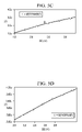
- FIG. 3C includes current and voltage data illustrated in tabular and graphical form for the POR 220 circuit operating in a post-trip region 306 , according to an embodiment.
- the data included in a table 350 and a graph 360 is computed using various techniques including use of testing, empirical, simulation tools, and similar others.
- the configured values for the POR 220 circuit provide the desired circuit performance such as power consumption, silicon area, output voltage level, and temperature invariance over the desired temperature range.
- the POR 220 circuit changes the value of the output voltage 222 .
- the emitter of the second transistor 264 carries less current compared to the emitter current of the first transistor 262 .
- the voltage at the first node 256 increases to about 0.631 volts, which is above the onset voltage of about 0.6 volts for full conduction of the third transistor 280 .
- the output voltage 222 is at a third voltage level that is equal to about 0.075 volt.
- the voltage across the third resistor 270 is about 0.0532 volts and the third transistor 280 is fully conducting due to the first node 256 being at 0.631 volts. Since the third transistor 280 is fully conducting, current between the first node 256 and the voltage reference 290 is split between three parallel paths in proportion to the resistance in each path. Therefore, the third transistor 280 carries significantly higher current compared to the current flowing through the second resistor 254 and the third resistor 270 .
- FIG. 4A illustrate in graphical form process and temperature variance data for the POR 220 circuit, according to an embodiment.
- FIG. 4B illustrates in graphical form process and temperature variance data for the traditional BPOR 100 .
- FIG. 4C illustrates in graphical form process and component mismatch variance data for the POR 220 circuit at ⁇ 40, 27, 87 and 150 degrees Celsius temperatures, according to an embodiment.
- FIG. 4D illustrates in graphical form process and component mismatch variance data for the traditional BPOR 100 at ⁇ 40, 27, 87 and 150 degrees Celsius temperatures.
- the performance of the POR 220 circuit may be benchmarked with the performance of the traditional BPOR 100 described with reference to FIG. 1 .
- the traditional BPOR 100 deploys 4 resistors (2 matched pairs) and 3 current mirrors compared to 3 resistors and 1 current mirror for the POR 220 circuit.
- the performance of the traditional BPOR 100 includes 250 millivolts three sigma variation at room temperature, a silicon area of about 8000 square micro meters (including 5000 for BJT's and 2500 for resistors).
- the performance of the POR 220 circuit includes 213 millivolts three sigma variation at room temperature, a silicon area of about 7600 square micro meters (including 5000 for BJT's and 1700 for resistors). Even though the POR 220 circuit has a lower delta base-to-emitter voltage (a higher value is typically more immune to mismatch) the POR 220 circuit consumes less power and has less trip-point variation with a lower silicon area compared to the traditional BPOR 100 . Thus, the POR 220 circuit provides less process and temperature variation and occupies less silicon area for the same power consumption as the BPOR 100 . Other trade offs such as same silicon area but reduced temperature variation and reduce current are also possible with the POR 220 circuit, as described with reference to FIGS.
- a silicon area of the POR 220 circuit is smaller than a comparable silicon area for a BPOR having the same desired trip point voltage and the desired current consumption.
- the POR 220 circuit provides additional headroom for the supply voltage compared to the BPOR 100 since the base voltage of the BJT's is base-to-emitter for the POR 220 and is bandgap voltage for the BPOR 100 . That is, more supply voltage is available for the current mirrors for the POR 220 circuit compared to the traditional BPOR 100 .
- FIG. 5A illustrate in graphical form process and temperature variance data for the POR 220 circuit that is optimized to reduce current and temperature variance for the same silicon area as the BPOR 100 , according to an embodiment.
- FIG. 5B illustrates in graphical form process and component mismatch variance data for the POR 220 circuit that is optimized to reduce current and temperature variance for the same silicon area as the BPOR 100 at ⁇ 40, 27, 87 and 150 degrees Celsius temperatures, according to an embodiment.
- FIG. 5C illustrate in graphical form current consumption data for the POR 220 circuit that is optimized to reduce current and temperature variance for the same silicon area as the BPOR 100 , according to an embodiment.
- FIG. 5D illustrates in graphical form current consumption data for the traditional BPOR 100 .
- the POR 220 is configured to have the same silicon area as the BPOR 100 but uses a reduced current and exhibits less temperature variation compared to the BPOR 100 .
- the performance of the POR 220 circuit that is optimized to reduce current and temperature variance for the same silicon area as the BPOR 100 includes 173 millivolts three sigma variation at room temperature which is less than the 213 mV three sigma variation for the POR 220 circuit described with reference to FIG. 4A .
- the BPOR 100 has a higher overall resistance compared to the overall resistance of the POR 220 circuit.
- the PTAT current is defined by a 100K ohm resistor (coupled to the transistor having the greater emitter area) and, about 6 times that resistor (about 590K ohms) is required to achieve a bandgap-referenced operation.
- the current consumption for the POR 220 is about 25% to 35% lower (depending on the selection of particular component values, dimensions, and similar other parameters) at the trip point compared to the BPOR 100 , the POR 220 circuit and the BPOR 100 being configured to have a common desired trip point voltage.
- the current consumption for the POR 220 circuit is about 2.213 microamperes compared to 3.409 microamperes for the BPOR 100 circuit, thereby resulting in a 35% reduction.
- the embodiments advantageously provide an improved POR circuit that deploys 3 resistors compared to the 4 resistors included in a traditional BPOR.
- the improved POR circuit advantageously provides tradeoffs between power consumption and silicon area compared to the traditional BPOR.
- the current consumption of the improved POR circuit is 25% lower compared to a current consumption of a BPOR, with the POR circuit and the BPOR being configured to have a common desired trip point voltage.
- a silicon area of the improved POR circuit is smaller than a comparable silicon area for a BPOR having the same desired trip point voltage and the desired current consumption.
Abstract
Description
Vtrip=(1+R2/R1)*[Vbe+M*Vptat*(R1∥R2)/R3]
where Vtrip=the output voltage, R2=
Claims (20)
Priority Applications (1)
| Application Number | Priority Date | Filing Date | Title |
|---|---|---|---|
| US12/343,326 US7821307B2 (en) | 2008-12-23 | 2008-12-23 | Bandgap referenced power on reset (POR) circuit with improved area and power performance |
Applications Claiming Priority (1)
| Application Number | Priority Date | Filing Date | Title |
|---|---|---|---|
| US12/343,326 US7821307B2 (en) | 2008-12-23 | 2008-12-23 | Bandgap referenced power on reset (POR) circuit with improved area and power performance |
Publications (2)
| Publication Number | Publication Date |
|---|---|
| US20100156477A1 US20100156477A1 (en) | 2010-06-24 |
| US7821307B2 true US7821307B2 (en) | 2010-10-26 |
Family
ID=42265085
Family Applications (1)
| Application Number | Title | Priority Date | Filing Date |
|---|---|---|---|
| US12/343,326 Active 2029-04-28 US7821307B2 (en) | 2008-12-23 | 2008-12-23 | Bandgap referenced power on reset (POR) circuit with improved area and power performance |
Country Status (1)
| Country | Link |
|---|---|
| US (1) | US7821307B2 (en) |
Cited By (11)
| Publication number | Priority date | Publication date | Assignee | Title |
|---|---|---|---|---|
| US20120105108A1 (en) * | 2010-10-28 | 2012-05-03 | Freescale Semiconductor, Inc. | Brown-out detection circuit |
| US20120229182A1 (en) * | 2011-03-07 | 2012-09-13 | Chih-Cheng Lin | Signal generating apparatus for generating power-on-reset signal |
| US8278995B1 (en) * | 2011-01-12 | 2012-10-02 | National Semiconductor Corporation | Bandgap in CMOS DGO process |
| CN103455118A (en) * | 2012-05-03 | 2013-12-18 | 德克萨斯仪器股份有限公司 | Detection of fast supply ramp in reset circuit |
| US9385689B1 (en) | 2015-10-13 | 2016-07-05 | Freescale Semiconductor, Inc. | Open loop band gap reference voltage generator |
| US9628071B2 (en) | 2013-04-04 | 2017-04-18 | Samsung Electronics Co., Ltd. | Power-on reset circuit and display device using power-on reset circuit |
| TWI605325B (en) * | 2016-11-21 | 2017-11-11 | 新唐科技股份有限公司 | Current source circuit |
| US20190086474A1 (en) * | 2017-09-20 | 2019-03-21 | Stmicroelectronics International N.V. | Circuitry for testing non-maskable voltage monitor for power management block |
| US11296692B1 (en) | 2021-04-30 | 2022-04-05 | Nxp B.V. | Power-on reset circuit |
| US11520364B2 (en) | 2020-12-04 | 2022-12-06 | Nxp B.V. | Utilization of voltage-controlled currents in electronic systems |
| US11838012B2 (en) | 2020-04-29 | 2023-12-05 | Ams International Ag | Power on reset circuit and integrated circuit including the same |
Families Citing this family (12)
| Publication number | Priority date | Publication date | Assignee | Title |
|---|---|---|---|---|
| US8262286B2 (en) * | 2008-11-18 | 2012-09-11 | Toshiba America Electronic Components, Inc. | Digital output temperature sensor |
| US7952402B2 (en) * | 2009-02-06 | 2011-05-31 | Standard Microsystems Corporation | Power-up control for very low-power systems |
| US20110063089A1 (en) * | 2009-09-11 | 2011-03-17 | Hynix Semiconductor Inc. | Radio frequency identification (rfid) system |
| KR101639352B1 (en) * | 2010-02-10 | 2016-07-13 | 삼성전자주식회사 | Transmitter detecting power-down of receiver automatically and System having the same |
| KR101782137B1 (en) * | 2010-11-08 | 2017-09-27 | 삼성전자주식회사 | Power on reset circuit |
| CN102291110B (en) * | 2011-06-21 | 2013-01-02 | 东南大学 | Power-on-reset circuit with zero steady state current consumption and stable pull-up voltage |
| CN102638183A (en) * | 2012-04-12 | 2012-08-15 | 泉芯电子技术(深圳)有限公司 | Flyback circuit control system and controller chip thereof |
| US9882558B1 (en) * | 2015-07-07 | 2018-01-30 | Marvell International Ltd. | Power-on reset circuit |
| CN105141119B (en) * | 2015-10-10 | 2018-01-05 | 上海灿瑞科技股份有限公司 | A kind of upper electricity is reset and under-voltage locking start-up circuit |
| DE102019002624A1 (en) * | 2019-04-10 | 2020-10-15 | Infineon Technologies Ag | Electronic circuit and method for initializing an electronic circuit |
| IT202000006109A1 (en) | 2020-03-23 | 2021-09-23 | St Microelectronics Srl | START-UP RESET CIRCUIT WITH IMPROVED ELECTRICAL FEATURES AND CORRESPONDING ELECTRONIC DEVICE |
| TWI736350B (en) * | 2020-07-07 | 2021-08-11 | 瑞昱半導體股份有限公司 | Voltage reduction circuit for bandgap reference voltage circuit |
Citations (2)
| Publication number | Priority date | Publication date | Assignee | Title |
|---|---|---|---|---|
| US7190212B2 (en) * | 2004-06-08 | 2007-03-13 | Saifun Semiconductors Ltd | Power-up and BGREF circuitry |
| US7411443B2 (en) | 2005-12-02 | 2008-08-12 | Texas Instruments Incorporated | Precision reversed bandgap voltage reference circuits and method |
-
2008
- 2008-12-23 US US12/343,326 patent/US7821307B2/en active Active
Patent Citations (2)
| Publication number | Priority date | Publication date | Assignee | Title |
|---|---|---|---|---|
| US7190212B2 (en) * | 2004-06-08 | 2007-03-13 | Saifun Semiconductors Ltd | Power-up and BGREF circuitry |
| US7411443B2 (en) | 2005-12-02 | 2008-08-12 | Texas Instruments Incorporated | Precision reversed bandgap voltage reference circuits and method |
Cited By (16)
| Publication number | Priority date | Publication date | Assignee | Title |
|---|---|---|---|---|
| US8253453B2 (en) * | 2010-10-28 | 2012-08-28 | Freescale Semiconductor, Inc. | Brown-out detection circuit |
| US20120105108A1 (en) * | 2010-10-28 | 2012-05-03 | Freescale Semiconductor, Inc. | Brown-out detection circuit |
| US8278995B1 (en) * | 2011-01-12 | 2012-10-02 | National Semiconductor Corporation | Bandgap in CMOS DGO process |
| US20120229182A1 (en) * | 2011-03-07 | 2012-09-13 | Chih-Cheng Lin | Signal generating apparatus for generating power-on-reset signal |
| US9059708B2 (en) | 2011-03-07 | 2015-06-16 | Realtek Semiconductor Corp. | Signal generating apparatus for generating power-on-reset signal |
| CN103455118B (en) * | 2012-05-03 | 2018-04-13 | 德克萨斯仪器股份有限公司 | The quickly detection on power supply slope in reset circuit |
| CN103455118A (en) * | 2012-05-03 | 2013-12-18 | 德克萨斯仪器股份有限公司 | Detection of fast supply ramp in reset circuit |
| US9628071B2 (en) | 2013-04-04 | 2017-04-18 | Samsung Electronics Co., Ltd. | Power-on reset circuit and display device using power-on reset circuit |
| US9385689B1 (en) | 2015-10-13 | 2016-07-05 | Freescale Semiconductor, Inc. | Open loop band gap reference voltage generator |
| TWI605325B (en) * | 2016-11-21 | 2017-11-11 | 新唐科技股份有限公司 | Current source circuit |
| US10620657B2 (en) | 2016-11-21 | 2020-04-14 | Nuvoton Technology Corporation | Current source circuit providing bias current unrelated to temperature |
| US20190086474A1 (en) * | 2017-09-20 | 2019-03-21 | Stmicroelectronics International N.V. | Circuitry for testing non-maskable voltage monitor for power management block |
| US10620267B2 (en) * | 2017-09-20 | 2020-04-14 | Stmicroelectronics International N.V. | Circuitry for testing non-maskable voltage monitor for power management block |
| US11838012B2 (en) | 2020-04-29 | 2023-12-05 | Ams International Ag | Power on reset circuit and integrated circuit including the same |
| US11520364B2 (en) | 2020-12-04 | 2022-12-06 | Nxp B.V. | Utilization of voltage-controlled currents in electronic systems |
| US11296692B1 (en) | 2021-04-30 | 2022-04-05 | Nxp B.V. | Power-on reset circuit |
Also Published As
| Publication number | Publication date |
|---|---|
| US20100156477A1 (en) | 2010-06-24 |
Similar Documents
| Publication | Publication Date | Title |
|---|---|---|
| US7821307B2 (en) | Bandgap referenced power on reset (POR) circuit with improved area and power performance | |
| US6799889B2 (en) | Temperature sensing apparatus and methods | |
| US20070086807A1 (en) | Image forming apparatus with detachable power-requiring unit | |
| US7420792B2 (en) | Linear charger where the material temperature directly affects the circuit thermal control | |
| US10296026B2 (en) | Low noise reference voltage generator and load regulator | |
| US8723554B2 (en) | High-stability reset circuit for monitoring supply undervoltage and overvoltage | |
| EP3565120B1 (en) | Circuit and method for reducing current leakage during a low-power or inactive mode | |
| US7242565B2 (en) | Thermal shut-down circuit | |
| TWI651609B (en) | Low voltage locking circuit and device thereof integrated with reference voltage generating circuit | |
| US8638127B2 (en) | Temperature-independent undervoltage detector and related method | |
| WO2006069157A2 (en) | Temperature-stable voltage reference circuit | |
| US20090224804A1 (en) | Detecting circuit and electronic apparatus using detecting circuit | |
| US5519341A (en) | Cross coupled quad comparator for current sensing independent of temperature | |
| US7642840B2 (en) | Reference voltage generator circuit | |
| US9385689B1 (en) | Open loop band gap reference voltage generator | |
| KR101551705B1 (en) | Reference voltage generating circuit | |
| TWI792988B (en) | Voltage generating circuit and semiconductor device | |
| US11296680B2 (en) | Methods and apparatus to implement temperature insensitive threshold detection for voltage supervisors | |
| US7321484B2 (en) | Providing accurate detection of chip overheat and local overheat conditions in integrated circuits | |
| US9519303B2 (en) | Precision current sensing | |
| TW202204906A (en) | Undervoltage detection circuit | |
| US20220360260A1 (en) | Circuit for preventing latch-up and integrated circuit | |
| CN106452401B (en) | Multi-junction semiconductor circuit and method | |
| JP2023520815A (en) | Bias current generation circuit and flash memory | |
| KR20240012328A (en) | Bandgap reference voltage generation circuit and semiconductor device with the same |
Legal Events
| Date | Code | Title | Description |
|---|---|---|---|
| AS | Assignment |
Owner name: TEXAS INSTRUMENTS INCORPORATED,TEXAS Free format text: ASSIGNMENT OF ASSIGNORS INTEREST;ASSIGNOR:CHELLAPPA, ANANTHASAYANAM;REEL/FRAME:022045/0398 Effective date: 20081222 Owner name: TEXAS INSTRUMENTS INCORPORATED, TEXAS Free format text: ASSIGNMENT OF ASSIGNORS INTEREST;ASSIGNOR:CHELLAPPA, ANANTHASAYANAM;REEL/FRAME:022045/0398 Effective date: 20081222 |
|
| STCF | Information on status: patent grant |
Free format text: PATENTED CASE |
|
| FPAY | Fee payment |
Year of fee payment: 4 |
|
| MAFP | Maintenance fee payment |
Free format text: PAYMENT OF MAINTENANCE FEE, 8TH YEAR, LARGE ENTITY (ORIGINAL EVENT CODE: M1552) Year of fee payment: 8 |
|
| MAFP | Maintenance fee payment |
Free format text: PAYMENT OF MAINTENANCE FEE, 12TH YEAR, LARGE ENTITY (ORIGINAL EVENT CODE: M1553); ENTITY STATUS OF PATENT OWNER: LARGE ENTITY Year of fee payment: 12 |