US7809334B2 - Signal transmitting and receiving apparatus capable of preventing the receiving end from saturating - Google Patents
Signal transmitting and receiving apparatus capable of preventing the receiving end from saturating Download PDFInfo
- Publication number
- US7809334B2 US7809334B2 US11/549,976 US54997606A US7809334B2 US 7809334 B2 US7809334 B2 US 7809334B2 US 54997606 A US54997606 A US 54997606A US 7809334 B2 US7809334 B2 US 7809334B2
- Authority
- US
- United States
- Prior art keywords
- signal
- oscillating
- receiving unit
- receiving
- transmitting
- Prior art date
- Legal status (The legal status is an assumption and is not a legal conclusion. Google has not performed a legal analysis and makes no representation as to the accuracy of the status listed.)
- Active, expires
Links
Images


Classifications
-
- G—PHYSICS
- G06—COMPUTING OR CALCULATING; COUNTING
- G06K—GRAPHICAL DATA READING; PRESENTATION OF DATA; RECORD CARRIERS; HANDLING RECORD CARRIERS
- G06K7/00—Methods or arrangements for sensing record carriers, e.g. for reading patterns
- G06K7/0008—General problems related to the reading of electronic memory record carriers, independent of its reading method, e.g. power transfer
Definitions
- the present invention relates to a signal transmitting and receiving apparatus and the method thereof, especially to a signal transmitting and receiving apparatus capable of preventing the receiving end from saturating and the corresponding method.
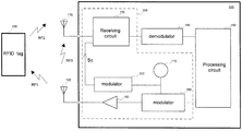
- FIG. 1 illustrates an application circuit for Radio Frequency Identification (RFID) technology.
- a reader 100 includes a receiving circuit 130 , a demodulator 140 , a processing circuit 150 , a modulator 160 , an oscillator 170 and a power amplifier 180 .
- the receiving circuit 130 receives RF signal through the antenna 110 and the power amplifier 180 emits RF signal through the antenna 120 .
- the modulator 160 modulates an oscillating signal generated by the oscillator 170 according to the control signal of the processing circuit 150 to form a modulated signal and the modulated signal is then amplified by the power amplifier 180 before being emitted through the antenna 120 .
- the RFID tag 200 receives the RF signal RF 1 from the antenna 120 and reflects an RF signal RF 2 to the reader 100 after processing the signal RF 1 .
- the reflection RF signal RF 2 is transmitted to the antenna 110 and then received by the receiving circuit 130 .
- the signal RF 2 is further processed by the processing circuit 150 .
- the RF signal emitted through the antenna 120 will be transmitted to only the RFID tag 200 ; however in practice, a portion of the leakage RF signal, RF 3 , will be received by the antenna 110 .
- signals amplified by the power amplifier 180 possess larger power (e.g., 30 dBm).
- the antenna isolation is not good enough (e.g., 25 dB to 30 dB)
- the receiving circuit 130 will probably saturate upon receiving the high-power leakage signal RF 3 .
- the reader 100 fails since the receiving circuit 130 is not able to receive the reflection signal RF 2 having a power of e.g., ⁇ 80 dBm.
- a signal transmitting and receiving apparatus includes a signal receiving unit, a a first signal generator, and a second signal generator.
- the signal receiving unit receives a first signal and a second signal.
- the first signal generator generates the first signal.
- the second signal generator which is coupled to the signal receiving unit, generates the second signal. There is a phase difference between the second signal and the first signal such that in the signal receiving unit the first signal and the second signal eliminate each other's power.
- a method for receiving and transmitting a signal includes: generating a first signal; generating a second signal; and transmitting the first signal and the second signal to a signal receiving unit. There is a phase difference between the second signal and the first signal such that in the signal receiving unit the first signal and the second signal eliminate each other's power.
- an RFID reader is disclosed.
- the RFID reader is characterized by including a receiving unit, an oscillator, a first modulator, a power amplifier, and a second modulator.
- the receiving unit receives a first signal and a second signal.
- the oscillator generates an oscillating signal.
- the first modulator which is coupled to the oscillator, modulates the oscillating signal to generate the first signal.
- the power amplifier which is coupled to the first modulator, amplifies the first signal.
- the second modulator which is coupled to the oscillator and the receiving unit, modulates the oscillating signal to generate the second signal. There is a phase difference between the second signal and the first signal such that in the signal receiving unit the first signal and the second signal eliminate each other's power.
- FIG. 1 is an application circuit for RFID technology.
- FIG. 2 is a signal transmitting and receiving apparatus capable of preventing the receiving end from saturating according to a first embodiment of the present invention.
- FIG. 3 is a signal transmitting and receiving apparatus capable of preventing the receiving end from saturating according to a second embodiment of the present invention.
- FIG. 2 shows the signal transmitting and receiving apparatus according to a first embodiment of this invention.
- the reader 300 includes a receiving circuit 130 , a demodulator 140 , a processing circuit 150 , a modulator 160 , an oscillator 170 , a power amplifier 180 , and a modulator 310 .
- the receiving circuit 130 receives signal through the antenna 110 , and the power amplifier 180 emits signal through the antenna 120 .
- the receiving circuit 130 , the modulator 160 , the oscillator 170 , the power amplifier 180 and the modulator 310 form the signal transmitting and receiving circuit 305 of this present invention.
- the elements of the reader 300 possess the same function as those designated by the same number of the reader 100 .
- the difference between the reader 300 and the reader 100 is that the reader 300 has a modulator 310 , which is coupled to the receiving circuit 130 for modulating an oscillating signal generated by the oscillator 170 . Then, the modulated signal Sc generated by the modulator 310 is transmitted to the receiving circuit 130 through a conductive wire in order to attenuate the RF signal RF 3 transmitted through wireless transmission.
- the oscillating signal generated by the oscillator 170 is assumed to be represented in the form of cos(w c t+ ⁇ ).
- the modulator 160 modulates the oscillating signal in the form of A 1 cos(w m t)cos(w c t+ ⁇ ) to carry the command. It is noted that the RFID tag 200 does not yet reflect the reflecting signal RF 2 to the antenna 110 at that time.
- the modulator 160 stops modulating, and then the reader 300 keeps emitting an RF signal to provide power to the RFID tag 200 .
- the receiving circuit 130 is ready to receive the reflection signal RF 2 . It is assumed that the signal which is utilized to power the RFID tag 200 and carries no command is represented in the form of A 2 cos(w c t+ ⁇ ).
- the modulator 310 modulates the oscillating signal such that the modulated signal Sc has the same frequency and a 180 degree phase difference with respect to the RF signal RF 3 . Furthermore, by adjusting the amplitude of the signal Sc to be close to the amplitude of the RF signal RF 3 , these two signals will eliminate each other's power when they are received by the receiving circuit 130 because of the phase difference and amplitudes. As a result, the receiving circuit 130 will not saturate due to the reception of the high-power RF signal RF 3 .
- one of the modulating methods of the modulator 310 is to adjust amplitude and phase of the oscillating signal.
- the receiving circuit 130 receives the RF signal RF 3 and the signal Sc at the same time.
- the leakage power from the antenna 120 to the antenna 110 can be eliminated by properly adjusting the amplitude B of the signal Sc to restrain the amplitude of the RF signal RF 3 .
- One of the main purposes of the modulator 310 is to adjust the phase of the oscillating signal, and it could be performed by several methods. In general, the phase adjustment can be implemented by the signal delay generated by a resistor connected in series with a capacitor or an inductor connected in series with a capacitor.
- FIG. 3 shows the signal transmitting and receiving apparatus according to a second embodiment of the present invention.
- the reader 400 includes a receiving circuit 130 , a demodulator 140 , a processing circuit 150 , a modulator 160 , an oscillator 170 , a power amplifier 180 , a modulator 310 and an oscillator 320 .
- the receiving circuit 130 receives signal through the antenna 110 , and the power amplifier 180 emits signal through the antenna 120 .
- the receiving circuit 130 , the modulator 160 , the oscillator 170 , the power amplifier 180 , the modulator 310 and the oscillator 320 form the signal transmitting and receiving circuit 405 of this present invention.
- the elements of the reader 400 possess the same function as those designated by the same number of the reader 300 .
- the difference between the reader 300 and the reader 400 is that in the reader 400 there is an additional oscillator 320 .
- the oscillator 320 and the oscillator 170 are synchronous by sharing the same reference source.
- the oscillator 320 is coupled to the modulator 310 for generating an oscillating signal different from the signal generated by the oscillator 170 .
- the oscillating signal generated by the oscillator 170 is referred to as the first oscillating signal
- the oscillating signal generated by the oscillator 320 is referred to as the second oscillating signal.
- the modulator 310 modulates the second oscillating signal and then transmits the modulated signal Sc to the receiving circuit 130 through a conductive wire in order that the signal Sc attenuates the RF signal RF 3 transmitted through wireless transmission.
- the modulator 310 modulates the frequency and the phase of the second oscillating signal to make the frequency of the signal Sc to be equal or close to the frequency of the RF signal RF 3 and also make the signal Sc has a 180 degree phase difference with respect to the RF signal RF 3 .
- the first and the second oscillating signals which are generated by the oscillator 170 and the oscillator 320 respectively, are represented in the form of cos(w c t+ ⁇ ).
- the modulator 160 modulates the oscillating signal in the form of A 1 cos(w m t)cos(w c t+ ⁇ ) to carry the command.
- the RFID tag 200 does not yet reflect the reflecting signal RF 2 to the antenna 110 at that time.
- the modulator 160 stops modulating, and then the reader 400 keeps emitting an RF signal to provide power to the RFID tag 200 .
- the receiving circuit 130 is ready to receive the reflection signal RF 2 .
- the signal which is utilized to power the RFID tag 200 and carries no command is represented in the form of A 2 cos(w c t+ ⁇ ).
- the modulator 310 modulates the second oscillating signal such that the modulated signal Sc has the same frequency and a 180 degree phase difference with respect to the RF signal RF 3 .
- the amplitude of the signal Sc will eliminate each other's power when they are received by the receiving circuit 130 because of the phase difference and amplitudes. As a result, the receiving circuit 130 will not saturate due to the reception of the high-power RF signal RF 3 .
- one of modulating methods of the modulator 310 is to adjust the frequency, phase and amplitude of the second oscillating signal.
- the receiving circuit 130 receives the RF signal RF 3 and the signal Sc at the same time.
- the leakage power from the antenna 120 to the antenna 110 can be eliminated by properly adjusting the amplitude B of the signal Sc to restrain the amplitude of RF signal RF 3 .
- One of the main purposes of the modulator 310 is to adjust the phase of the oscillating signal, and it could be performed by several methods. In general, the phase adjustment can be implemented by the signal delay generated by a resistor connected in series with a capacitor or an inductor connected in series with a capacitor.
- an emitting signal from the transmitting end of a signal transmitting and receiving apparatus might be received unexpectedly by the receiving end. If the power of the emitting signal is larger than the capacity of the receiving end, the receiving end will saturate and therefore is not able to receive signals with small power. This kind of problem is usually encountered by an RFID reader.
- the present invention discloses a method and the corresponding apparatus to solve this problem.
- the signal transmitting and receiving apparatus is provided with a modulator coupled to the receiving end for generating a modulated signal.
- the modulated signal is then transmitted through a conductive wire to the receiving end to eliminate the leakage signal from the transmitting end. As a result, the receiving end will not saturate.
Landscapes
- Engineering & Computer Science (AREA)
- Artificial Intelligence (AREA)
- Computer Vision & Pattern Recognition (AREA)
- Physics & Mathematics (AREA)
- General Physics & Mathematics (AREA)
- Theoretical Computer Science (AREA)
- Near-Field Transmission Systems (AREA)
- Radar Systems Or Details Thereof (AREA)
Abstract
Description
The receiving
According to the above equation, the leakage power from the
The receiving
According to the above equation, the leakage power from the
Claims (19)
Applications Claiming Priority (3)
| Application Number | Priority Date | Filing Date | Title |
|---|---|---|---|
| TW095118247A TWI314402B (en) | 2006-05-23 | 2006-05-23 | Signal transmitting and receiving apparatus capable of preventing the receiving end from saturating |
| TW95118247A | 2006-05-23 | ||
| TW095118247 | 2006-05-23 |
Publications (2)
| Publication Number | Publication Date |
|---|---|
| US20070275673A1 US20070275673A1 (en) | 2007-11-29 |
| US7809334B2 true US7809334B2 (en) | 2010-10-05 |
Family
ID=38750115
Family Applications (1)
| Application Number | Title | Priority Date | Filing Date |
|---|---|---|---|
| US11/549,976 Active 2029-06-23 US7809334B2 (en) | 2006-05-23 | 2006-10-17 | Signal transmitting and receiving apparatus capable of preventing the receiving end from saturating |
Country Status (2)
| Country | Link |
|---|---|
| US (1) | US7809334B2 (en) |
| TW (1) | TWI314402B (en) |
Cited By (1)
| Publication number | Priority date | Publication date | Assignee | Title |
|---|---|---|---|---|
| US20130040582A1 (en) * | 2010-04-27 | 2013-02-14 | Nec Corporation | Wireless communication device, high-frequency circuit system, and local leak reduction method |
Families Citing this family (2)
| Publication number | Priority date | Publication date | Assignee | Title |
|---|---|---|---|---|
| KR100932064B1 (en) * | 2007-09-04 | 2009-12-15 | 한국전자통신연구원 | RDF tag and its control method |
| US11238247B2 (en) * | 2015-04-13 | 2022-02-01 | Rfid Technologies Pty Ltd | RFID tag and reader |
Citations (8)
| Publication number | Priority date | Publication date | Assignee | Title |
|---|---|---|---|---|
| US5444864A (en) * | 1992-12-22 | 1995-08-22 | E-Systems, Inc. | Method and apparatus for cancelling in-band energy leakage from transmitter to receiver |
| EP0905914A2 (en) | 1997-08-27 | 1999-03-31 | Shin-A Telecom | Apparatus for cancelling radio frequency interference between transmitting antenna and receiving antenna, repeating system and transmitting and receiving system using the same |
| US5974301A (en) * | 1996-09-18 | 1999-10-26 | Ludwig Kipp | Frequency cancelling system and method |
| US6311045B1 (en) | 1997-07-28 | 2001-10-30 | Roke Manor Research Limited | Apparatus for signal isolation in a radio transmitter-receiver |
| US6539204B1 (en) * | 2000-09-29 | 2003-03-25 | Mobilian Corporation | Analog active cancellation of a wireless coupled transmit signal |
| US20030080862A1 (en) | 2001-10-31 | 2003-05-01 | Kranz Mark J. | Tire pressure monitoring system |
| US6567649B2 (en) * | 2000-08-22 | 2003-05-20 | Novatel Wireless, Inc. | Method and apparatus for transmitter noise cancellation in an RF communications system |
| US20060252398A1 (en) * | 2005-05-09 | 2006-11-09 | Park Kyung H | Receiver of RFID reader for eliminating leakage signal |
-
2006
- 2006-05-23 TW TW095118247A patent/TWI314402B/en not_active IP Right Cessation
- 2006-10-17 US US11/549,976 patent/US7809334B2/en active Active
Patent Citations (8)
| Publication number | Priority date | Publication date | Assignee | Title |
|---|---|---|---|---|
| US5444864A (en) * | 1992-12-22 | 1995-08-22 | E-Systems, Inc. | Method and apparatus for cancelling in-band energy leakage from transmitter to receiver |
| US5974301A (en) * | 1996-09-18 | 1999-10-26 | Ludwig Kipp | Frequency cancelling system and method |
| US6311045B1 (en) | 1997-07-28 | 2001-10-30 | Roke Manor Research Limited | Apparatus for signal isolation in a radio transmitter-receiver |
| EP0905914A2 (en) | 1997-08-27 | 1999-03-31 | Shin-A Telecom | Apparatus for cancelling radio frequency interference between transmitting antenna and receiving antenna, repeating system and transmitting and receiving system using the same |
| US6567649B2 (en) * | 2000-08-22 | 2003-05-20 | Novatel Wireless, Inc. | Method and apparatus for transmitter noise cancellation in an RF communications system |
| US6539204B1 (en) * | 2000-09-29 | 2003-03-25 | Mobilian Corporation | Analog active cancellation of a wireless coupled transmit signal |
| US20030080862A1 (en) | 2001-10-31 | 2003-05-01 | Kranz Mark J. | Tire pressure monitoring system |
| US20060252398A1 (en) * | 2005-05-09 | 2006-11-09 | Park Kyung H | Receiver of RFID reader for eliminating leakage signal |
Cited By (2)
| Publication number | Priority date | Publication date | Assignee | Title |
|---|---|---|---|---|
| US20130040582A1 (en) * | 2010-04-27 | 2013-02-14 | Nec Corporation | Wireless communication device, high-frequency circuit system, and local leak reduction method |
| US8805286B2 (en) * | 2010-04-27 | 2014-08-12 | Nec Corporation | Wireless communication device, high-frequency circuit system, and local leak reduction method |
Also Published As
| Publication number | Publication date |
|---|---|
| TWI314402B (en) | 2009-09-01 |
| US20070275673A1 (en) | 2007-11-29 |
| TW200744327A (en) | 2007-12-01 |
Similar Documents
| Publication | Publication Date | Title |
|---|---|---|
| JP4387323B2 (en) | RFID transceiver | |
| US7369811B2 (en) | System and method for sensitivity optimization of RF receiver using adaptive nulling | |
| US20070066224A1 (en) | High efficiency RF amplifier and envelope modulator | |
| US20080030336A1 (en) | Semiconductor integrated circuit device and receiving device | |
| KR20080097115A (en) | Radio frequency identification device | |
| US7546137B2 (en) | Power control loop and LO generation method | |
| US7809334B2 (en) | Signal transmitting and receiving apparatus capable of preventing the receiving end from saturating | |
| US7039362B2 (en) | Wireless transceiver and method for remote ultrasonic measurements | |
| JP4604964B2 (en) | Transmission / reception device, modulation integrated circuit, and RFID reader / writer | |
| JP4516029B2 (en) | Reader / writer device | |
| US7095988B2 (en) | Apparatus for linear transmitter with improved loop gain stabilization | |
| JP2006295287A (en) | Carrier sense method and RFID transceiver device using the same | |
| JP7408373B2 (en) | Communication equipment, transmission parts and communication systems | |
| JP2008187227A (en) | Rfid reader | |
| KR100961672B1 (en) | Modulator device for electromagnetic signals transmitted by contactless transmission / reception system | |
| JP4095632B2 (en) | Interrogator | |
| KR101870389B1 (en) | Method and RF receiver for receiving in low-power short-range on IoT(internet of things) sensor network environment | |
| CN101083479B (en) | Signal transceiving device and method for preventing receiver saturation | |
| US7383026B1 (en) | Wideband retroreflector | |
| EP0649111A1 (en) | Noise reduction in identification system | |
| JP2008022045A (en) | Receiver, transmitter and data communication system | |
| JP2021044607A (en) | Wireless devices, self-diagnosis methods and programs for wireless devices | |
| JPH05252164A (en) | Local area network system | |
| JP2001358609A (en) | Interrogator |
Legal Events
| Date | Code | Title | Description |
|---|---|---|---|
| AS | Assignment |
Owner name: MSTAR SEMICONDUCTOR, INC., TAIWAN Free format text: ASSIGNMENT OF ASSIGNORS INTEREST;ASSIGNORS:CHEN, SHOUFANG;YANG, STEVE WIYI;REEL/FRAME:018396/0624 Effective date: 20061009 |
|
| STCF | Information on status: patent grant |
Free format text: PATENTED CASE |
|
| FPAY | Fee payment |
Year of fee payment: 4 |
|
| MAFP | Maintenance fee payment |
Free format text: PAYMENT OF MAINTENANCE FEE, 8TH YEAR, LARGE ENTITY (ORIGINAL EVENT CODE: M1552) Year of fee payment: 8 |
|
| AS | Assignment |
Owner name: MEDIATEK INC., TAIWAN Free format text: MERGER;ASSIGNOR:MSTAR SEMICONDUCTOR, INC.;REEL/FRAME:052931/0468 Effective date: 20190115 |
|
| AS | Assignment |
Owner name: XUESHAN TECHNOLOGIES INC., CANADA Free format text: ASSIGNMENT OF ASSIGNORS INTEREST;ASSIGNOR:MEDIATEK INC.;REEL/FRAME:055443/0818 Effective date: 20201223 |
|
| MAFP | Maintenance fee payment |
Free format text: PAYMENT OF MAINTENANCE FEE, 12TH YEAR, LARGE ENTITY (ORIGINAL EVENT CODE: M1553); ENTITY STATUS OF PATENT OWNER: LARGE ENTITY Year of fee payment: 12 |