US7804491B2 - Touch panel - Google Patents
Touch panel Download PDFInfo
- Publication number
- US7804491B2 US7804491B2 US11/790,743 US79074307A US7804491B2 US 7804491 B2 US7804491 B2 US 7804491B2 US 79074307 A US79074307 A US 79074307A US 7804491 B2 US7804491 B2 US 7804491B2
- Authority
- US
- United States
- Prior art keywords
- conductive layer
- touch panel
- substrate
- electrodes
- slit
- Prior art date
- Legal status (The legal status is an assumption and is not a legal conclusion. Google has not performed a legal analysis and makes no representation as to the accuracy of the status listed.)
- Expired - Fee Related, expires
Links
Images


Classifications
-
- G—PHYSICS
- G06—COMPUTING; CALCULATING OR COUNTING
- G06F—ELECTRIC DIGITAL DATA PROCESSING
- G06F3/00—Input arrangements for transferring data to be processed into a form capable of being handled by the computer; Output arrangements for transferring data from processing unit to output unit, e.g. interface arrangements
- G06F3/01—Input arrangements or combined input and output arrangements for interaction between user and computer
- G06F3/03—Arrangements for converting the position or the displacement of a member into a coded form
- G06F3/041—Digitisers, e.g. for touch screens or touch pads, characterised by the transducing means
- G06F3/045—Digitisers, e.g. for touch screens or touch pads, characterised by the transducing means using resistive elements, e.g. a single continuous surface or two parallel surfaces put in contact
Definitions
- the present invention mainly relates to a touch panel used for an operation of various electronic devices.
- a conventional touch panel will be described with reference to FIG. 8 to FIG. 10 .
- FIG. 8 is a cross-sectional view illustrating a conventional touch panel.
- FIG. 9 is a plan view illustrating an upper substrate used for the touch panel shown in FIG. 8 .
- FIG. 10 is a plan view illustrating a lower substrate used for the touch panel shown in FIG. 8 .
- upper substrate 101 has a film-like shape and is optically-transparent.
- Upper substrate 101 has, at a lower side thereof, optically-transparent lower substrate 102 .
- optically-transparent upper conductive layer 103 is formed by material such as indium tin oxide.
- optically-transparent lower conductive layer 104 is similarly formed by material such as indium tin oxide for example.
- Both ends of upper conductive layer 103 have a pair of upper electrodes 105 , 106 . Both ends of lower conductive layer 104 have a pair of lower electrodes 107 , 108 formed in a direction orthogonal to upper electrodes 105 , 106 .
- Upper electrodes 105 , 106 extend along an outer periphery of upper conductive layer 103 . End of upper substrate 101 has a plurality of lead sections 105 a , 106 a .
- Lower electrodes 107 , 108 extend along an outer periphery of lower conductive layer 104 . End of lower substrate 102 has a plurality of lead sections 107 a , 108 a . It is noted that upper electrodes 105 , 106 and lower electrodes 107 , 108 are made of conductive material including silver.
- Slit 109 is provided at an inner side of upper electrodes 105 , 106 and between lead sections 105 a , 106 a .
- Slit 109 having a substantially T-like shape is obtained by removing upper conductive layer 103 by a method including a laser cutting or an etching processing, for example.
- Slit 110 is also provided between lower electrodes 107 , 108 , and between lead sections 107 a , 108 a .
- Slit 110 having a substantially L-like shape is similarly obtained by removing lower conductive layer 104 by the method including a laser cutting or an etching processing, for example. This prevents the short circuiting between upper electrode 105 and upper electrode 106 , and between lower electrode 107 and lower electrode 108 , thereby securing insulation among the electrodes.
- Spacer 111 having a substantially frame-like shape is provided at an outer periphery of a lower face of upper substrate 101 or an outer periphery of an upper face of lower substrate 102 .
- An upper face and a lower face of spacer 111 are coated with adhesion layers (not shown).
- an outer periphery of upper substrate 101 is adhered with an outer periphery of lower substrate 102 and upper conductive layer 103 is facing to lower conductive layer 104 with a predetermined space therebetween. In this manner, touch panel 100 is provided.
- Touch panel 100 thus structured is placed on a front face of a liquid crystal display element (not shown) and others, and is attached to an electronic device.
- Lead sections 105 a , 106 a , 107 a , and 108 a provided at end sections of upper electrodes 105 , 106 and end sections of lower electrodes 107 , 108 are connected to an electronic circuit of an electronic device (not shown) via a wiring substrate (not shown) in which upper and lower faces have a plurality of wiring patterns, for example.
- an upper face of upper substrate 101 is depressed and operated by a finger or a pen while the display of a liquid crystal display element provided at the back face of touch panel 100 being visually recognized.
- upper substrate 101 is bent and upper conductive layer 103 at the depressed portion is come into contact with lower conductive layer 104 .
- a voltage is sequentially applied from the electronic circuit via the wiring substrate to upper electrodes 105 , 106 as well as lower electrodes 107 , 108 .
- the applied voltage is sequentially applied to the both ends of upper conductive layer 103 and the both ends of lower conductive layer 104 in a direction orthogonal to upper conductive layer 103 .
- the depressed position is detected by the electronic circuit. As a result, various functions of the electronic device are switched.
- slits 109 , 110 are formed by the method including a laser cutting or an etching processing as described above.
- a laser cut processing has been increasingly used in recent years because it provides a speedy manufacture.
- the processing is actually performed to cause protruded section 109 b , as shown in FIG. 9 , that inwardly protrudes from intersection 109 a having a substantially T-like shape.
- protruded section 109 b is caused by the control of a laser beam for machining slit 109 .
- this part When a strong force is applied to a position adjacent to intersection 109 a as shown in FIG. 9 or terminal section 110 a of slit 110 as shown in FIG. 10 for example, or when such a part is subjected to a depression operation repeated for a long time, this part may crack or break to cause a crack or breakage of upper conductive layer 103 and lower conductive layer 104 . This causes unstable electrical connection and separation between upper conductive layer 103 and lower conductive layer 104 .
- slit 109 is formed by a laser beam with a slowly controlled moving speed so that the laser beam does not move beyond intersection 109 a , although the moving speed causes a longer manufacture time.
- a part adjacent to intersection 109 a and a part adjacent to terminal section 110 a are covered by spacer 111 , although the existence of spacer 111 reduces an operation region, for example.
- a conventional touch panel is disclosed, for example, in Japanese Patent Unexamined Publication No. 2003-58319.
- the present invention provides a touch panel that provides stable electrical connection and separation by a simple structure.
- the touch panel of the present invention has a first optically-transparent substrate, a second optically transparent substrate, a slit, and a groove section.
- the first substrate has a first conductive layer and a plurality of first electrodes extending from both ends of the first conductive layer and having first electrode lead sections.
- the second substrate has a second conductive layer, and a plurality of second electrodes extending from both ends of the second conductive layer and having second electrode lead sections.
- the slit is formed in the first conductive layer and the second conductive layer, and has an intersection or a terminal section.
- the groove section is provided around the intersection or around the terminal section.
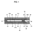
- FIG. 1 is a schematic sectional view illustrating a touch panel according to an embodiment of the present invention.
- FIG. 2 is a plan view illustrating an upper substrate used for the touch panel shown in FIG. 1 .
- FIG. 3 is a plan view illustrating a lower substrate used for the touch panel shown in FIG. 1 .
- FIG. 4 is an expanded plan view illustrating the main part of an upper substrate of another arrangement used for the touch panel according to an embodiment of the present invention.
- FIG. 5 is an expanded plan view illustrating the main part of a lower substrate of another arrangement used for the touch panel according to an embodiment of the present invention.
- FIG. 6 is an expanded plan view illustrating the main part of a lower substrate of another arrangement used for the touch panel according to an embodiment of the present invention.
- FIG. 7 is an expanded plan view illustrating the main part of a lower substrate of another arrangement used for the touch panel according to an embodiment of the present invention.
- FIG. 8 is a cross-sectional view illustrating a conventional touch panel.
- FIG. 9 is a plan view illustrating an upper substrate used for the conventional touch panel.
- FIG. 10 is a plan view illustrating a lower substrate used for the conventional touch panel.
- FIG. 1 is a schematic cross sectional view illustrating a touch panel according to an embodiment of the present invention.
- FIG. 2 is a plan view illustrating an upper substrate used for the touch panel shown in FIG. 1 .
- FIG. 3 is a plan view illustrating a lower substrate used for the touch panel shown in FIG. 1 . It is noted that, in the schematic cross sectional view of the touch panel shown in FIG. 1 , the cross section of the upper substrate is taken along cross section line 1 - 1 shown in FIG. 2 while the cross section of the lower substrate is taken along cross section line 1 - 1 shown in FIG. 3 .
- first substrate 21 is an upper substrate that has a film-like shape, that is optically-transparent, and that is made of optically-isotropic material such as polyethylene terephthalate or polycarbonate resin.
- Second substrate 22 is a lower substrate that is made of optically-isotropic material such as glass, acrylic resin, or polycarbonate resin and that is optically-transparent.
- First face 21 a which is a lower face of first substrate 21 , has first conductive layer 23 as an optically-transparent upper conductive layer.
- Second face 22 a which is an upper face of second substrate 22 , has second conductive layer 24 as an optically-transparent lower conductive layer.
- First conductive layer 23 and second conductive layer 24 are formed by material such as indium tin oxide or tin oxide by a method such as the sputter method for example, respectively.
- First conductive layer 23 and second conductive layer 24 formed by the sputter method or the like are modified to have a predetermined shape by a method such as a laser cut or etching processing.
- First electrodes 25 , 26 which are a pair of upper electrodes, are provided at both ends of first conductive layer 23 .
- second electrodes 27 , 28 are formed as a pair of lower electrodes.
- First electrodes 25 , 26 extend at an outer periphery of first conductive layer 23 and first electrode lead sections 25 a , 26 a are provided at end section 21 b of first substrate 21 .
- second electrodes 27 , 28 extend at an outer periphery of second conductive layer 24 and second electrode lead sections 27 a , 28 b are provided at end section 22 b of second substrate 22 .
- first electrodes 25 , 26 and second electrodes 27 , 28 are formed by conductive material such as silver or carbon.
- First electrodes 25 , 26 and second electrodes 27 , 28 form electrodes.
- First electrode lead sections 25 a , 26 a as well as second electrode lead sections 27 a , 28 a form an electrode lead section.
- First slit 29 having a substantially T-like shape is provided at an inner side of first electrodes 25 , 26 and between first electrode lead sections 25 a , 26 a .
- First slit 29 is obtained by removing first conductive layer 23 by a laser cutting or an etching processing, for example.
- second slit 30 having a substantially L-like shape is provided between second electrodes 27 , 28 and between second electrode lead sections 27 a , 28 a .
- Second slit 30 is obtained by removing second conductive layer 24 by a laser cutting or an etching processing, for example.
- the existence of first slit 29 suppresses the short-circuiting between first electrode 25 and first electrode 26 to maintain the insulation therebetween.
- second slit 30 suppresses the short-circuiting between second electrode 27 and second electrode 28 to maintain the insulation therebetween.
- First groove section 34 is provided to be adjacent to an inner side of intersection 29 a of first slit 29 at first substrate 21 .
- First groove section 34 is obtained by removing first conductive layer 23 by a laser cutting or an etching processing, for example.
- Second groove section 35 having a substantially L-like shape is provided to be adjacent to a periphery of terminal section 30 a of second slit 30 at second substrate 22 .
- Second groove section 35 is obtained by removing second conductive layer 24 by a laser cuffing or an etching processing, for example.
- First slit 29 and second slit 30 constitute slits
- first groove section 34 and second groove section 35 constitute groove sections.
- protruded section 29 b slightly inwardly protruding from intersection 29 a also may be provided.
- protruded section 29 b is caused by the control of a laser beam moved for machining first slit 29 , for example.
- Second conductive layer 24 has thereon a plurality of dot spacers (not shown) made by insulating resin (e.g., epoxy resin, silicone resin) with a predetermined interval thereamong.
- insulating resin e.g., epoxy resin, silicone resin
- Spacer 31 having a substantially frame-like shape is provided at an outer periphery of first face 21 a or at an outer periphery of second face 22 a .
- Spacer 31 made by material such as polyester resin or epoxy resin is formed by a method such as printing.
- Adhesion layer (not shown, e.g., acrylic resin, rubber) coated on either both sides or one side of an upper face and a lower face of spacer 31 adheres the outer periphery of first substrate 21 with the outer periphery of second substrate 22 .
- first conductive layer 23 is facing to second conductive layer 24 with a predetermined gap therebetween.
- Touch panel 20 is structured in the manner as described above. It is noted that the term “frame-like” herein means a frame-like shape including only the outer frame of a polygonal shape (e.g., quadrilateral shape).
- first conductive layer 23 and second conductive layer 24 are formed by the sputter method or the like. Then, a method (e.g., laser cut, etching processing) is used to remove first conductive layer 23 and second conductive layer 24 to form first slit 29 , second slit 30 , first groove section 34 and second groove section 35 . Then, a method such as printing is used to form first electrodes 25 , 26 , second electrodes 27 , 28 , first electrode lead sections 25 a , 26 b , and second electrode lead sections 27 a , 28 a.
- a method e.g., laser cut, etching processing
- Touch panel 20 thus structured is placed on a front face of a liquid crystal display element (not shown) or the like and is attached to an electronic device (not shown). Then, first electrode lead sections 25 a , 26 a as well as second electrode lead sections 27 a , 28 a are connected to an electronic circuit (not shown) of the electronic device, for example, via a wiring substrate (not shown) or the like having a plurality of wiring patterns in an upper face and a lower face.
- a user of the electronic device depresses and operates upper face 21 c of first substrate 21 by a finger or a pen for example while visually recognizing the display by the liquid crystal display element provided at a back face of touch panel 20 .
- first substrate 21 is bent to cause first conductive layer 23 at the depressed portion to be come into contact with second conductive layer 24 .
- first electrodes 25 , 26 and second electrodes 27 , 28 are sequentially applied from the electronic circuit via the wiring substrate to first electrodes 25 , 26 and second electrodes 27 , 28 , respectively.
- the voltages applied to first electrodes 25 , 26 and second electrodes 27 , 28 are sequentially applied to the both ends of first conductive layer 23 and the both ends of second conductive layer 24 in a direction orthogonal to the both ends of first conductive layer 23 , respectively.
- the depressed position is detected by the electronic circuit. As a result, various functions of the electronic device are switched.
- touch panel 20 When touch panel 20 is depressed and operated, a strong force may be applied to a part in the vicinity of intersection 29 a of first slit 29 or terminal section 30 a of second slit 30 . Alternatively, a depression operation may be repeated for a long time. Thus, a part in the vicinity pf intersection 29 a or terminal section 30 a may be cracked or broken to cause a crack or breakage of first conductive layer 23 and second conductive layer 24 .
- touch panel 20 has first groove section 34 in the vicinity of intersection 29 a and second groove section 35 in the vicinity of terminal section 30 a .
- first groove section 34 prevents, even when a crack or a breakage is caused in the vicinity of intersection 29 of first conductive layer 23 , a further crack or breakage to the inner side of first conductive layer 23 .
- second groove section 35 prevents a further crack or breakage to the inner side of second conductive layer 24 .
- intersection 29 a has a crack or a breakage
- the crack or breakage extends to first groove section 34 but does not expand further, and is prevented from expanding to the inner side of first conductive layer 23 .
- terminal section 30 a has a crack or a breakage
- the crack or breakage extends to second groove section 35 but does not expand further, and is prevented from expanding to the inner side of second conductive layer 24 . This prevents the crack or breakage from extending, due to an electrical connection of touch panel 20 , to the inner part of first conductive layer 23 or the inner part of second conductive layer 24 , thereby providing stable electrical connection and separation.
- first conductive layer 23 includes first slit 29 having a predetermined shape and first groove section 34 is provided in the vicinity of intersection 29 a of first slit 29 or at the periphery of intersection 29 a .
- first groove section 34 prevents a crack or a breakage from intersection 29 a from extending to the inner side of first conductive layer 23 .
- touch panel 20 can be obtained that provides stable electrical connection and separation of first conductive layer 23 by a simple structure.
- second conductive layer 24 includes second slit 30 having a predetermined shape.
- second groove section 35 is provided at the periphery of terminal section 30 a of second slit 30 or in the vicinity of terminal section 30 a .
- second groove section 35 prevents a crack or a breakage from terminal section 30 a from extending to the inner side of second conductive layer 24 .
- touch panel 20 can be obtained that provides stable electrical connection and separation of second conductive layer 24 by a simple structure.
- First groove section 34 and second groove section 35 are formed by a laser cut processing, for example, at the same time as the formation of first slit 29 or second slit 30 . This can eliminate an unnecessary machining time and thus realizes the manufacture of touch panel 20 with a low cost.
- first groove section 34 and second groove section 35 are provided both at the inner side of intersection 29 a of first slit 29 at first substrate 21 and at the periphery of terminal section 30 a of second slit 30 at second substrate 22 .
- first groove section 34 and second groove section 35 are not always required.
- the present invention also can be carried out by another structure in which, depending on the structure of touch panel 20 or an electronic device connected to touch panel 20 for example, an insulating groove is provided at any one of such groove sections that receives a concentrated force when touch panel 20 is depressed and operated.
- first electrodes 25 , 26 , second electrodes 27 , 28 , first slit 29 and second slit 30 are not limited to the above-described shapes and arrangements.
- second electrodes 27 , 28 and second slit 30 also may be provided in first substrate 21
- first electrodes 25 , 26 and first slit 29 also may be provided in second substrate 22 .
- first groove section 34 is also not limited to the above-described shape.
- first groove section 34 at the inner side of intersection 29 a also may be first groove section 34 a having a substantially umbrella-like shape or a substantially circular arc-like shape and thus may have various shapes.
- first groove section 34 has a curvature to the direction of intersection 29 a as in first groove section 34 a , an effect for suppressing a further crack or breakage from intersection 29 a is further improved.
- intersection 29 a or protruded section 29 b is positioned at the center of the circular arc of first groove section 34 a having a curvature, expansion of a crack or a breakage caused in the vicinity of intersection 29 a or protruded section 29 b can be efficiently suppressed.
- first groove section 34 has, as in first groove section 34 a , a shape to surround intersection 29 a or protruded section 29 b , a crack or a breakage caused in the vicinity of intersection 29 a or protruded section 29 b is suppressed from expanding in the respective directions.
- touch panel 20 can be obtained that can have further stable electrical connection and separation.
- second groove section 35 is not limited to the above-described shape.
- second groove section 35 around terminal section 30 a may be substantially U-like second groove section 35 a as shown in FIG. 5 or also may be substantially horseshoe-like or substantially C-like second groove section 35 b as shown in FIG. 6 .
- Second groove section 35 also may be substantially J-like second groove section 35 c as shown in FIG. 7 .
- various shapes can be used.
- second groove section 35 has a curvature in the direction of terminal section 30 a as in second groove sections 35 a , 35 b , and 35 c can further enhance the effect for suppressing a crack or breakage caused at terminal section 30 a from expanding.
- the structure in which terminal section 30 a is positioned at the center of the circular arc of second groove sections 35 a , 35 b , and 35 c having a curvature can efficiently suppress a crack or breakage caused in the vicinity of terminal section 30 a from expanding.
- terminal section 30 a suppresses a crack or a breakage caused in the vicinity of terminal section 30 a from expanding in the respective directions.
- touch panel 20 can be obtained that can have further stable electrical connection and separation.
- FIG. 4 is an expanded plan view illustrating the main part of an upper substrate of another embodiment.
- FIG. 4 is an expanded plan view illustrating the main part of part 42 of FIG. 2 .
- FIG. 5 , FIG. 6 , and FIG. 7 are an expanded plan views illustrating the main part of a lower substrate of another embodiment.
- FIG. 5 , FIG. 6 , and FIG. 7 are an expanded plan views illustrating the main part of part 43 of FIG. 3 .
- first electrodes 25 , 26 extend at the outer periphery of first conductive layer 23
- end section 21 b of first substrate 21 includes first electrode lead sections 25 a , 26 a
- second electrodes 27 , 28 extend at the outer periphery of second conductive layer 24
- end section 22 b of second substrate 22 includes second electrode lead sections 27 a , 28 a
- the present invention also can be applied to another structure in which any one of first electrode lead sections 25 a , 26 a or second electrode lead sections 27 a , 28 a is introduced via a through hole (e.g., silver, copper) and any of end section 21 b of first substrate 21 or end section 22 b of second substrate 22 includes four electrode lead sections.
- the four electrode lead sections include first electrode lead sections 25 a , 26 a and second electrode lead sections 27 a , 28 a.
- the above section also has described a structure in which the outer periphery of first substrate 21 and the outer periphery of second substrate 22 are adhered by spacer 31 and adhesion layer.
- the present invention is not always limited to the structure in which the outer periphery of first substrate 21 and the outer periphery of second substrate 22 are adhered by spacer 31 and adhesion layer.
- the invention also can be applied to another structure not using spacer 31 for example so long as the structure has first substrate 21 facing to second substrate 22 with a predetermined gap therebetween.
- Still another structure also may be used in which the outer periphery of first substrate 21 is adhered to the outer periphery of second substrate 22 by a two-sided tape having surfaces coated with adhesive agent (not shown).
Landscapes
- Engineering & Computer Science (AREA)
- General Engineering & Computer Science (AREA)
- Theoretical Computer Science (AREA)
- Human Computer Interaction (AREA)
- Physics & Mathematics (AREA)
- General Physics & Mathematics (AREA)
- Position Input By Displaying (AREA)
Abstract
Description
Claims (9)
Applications Claiming Priority (2)
| Application Number | Priority Date | Filing Date | Title |
|---|---|---|---|
| JP2006137542A JP4687561B2 (en) | 2006-05-17 | 2006-05-17 | Touch panel |
| JP2006-137542 | 2006-05-17 |
Publications (2)
| Publication Number | Publication Date |
|---|---|
| US20080170041A1 US20080170041A1 (en) | 2008-07-17 |
| US7804491B2 true US7804491B2 (en) | 2010-09-28 |
Family
ID=38843353
Family Applications (1)
| Application Number | Title | Priority Date | Filing Date |
|---|---|---|---|
| US11/790,743 Expired - Fee Related US7804491B2 (en) | 2006-05-17 | 2007-04-27 | Touch panel |
Country Status (3)
| Country | Link |
|---|---|
| US (1) | US7804491B2 (en) |
| JP (1) | JP4687561B2 (en) |
| CN (1) | CN100524186C (en) |
Cited By (3)
| Publication number | Priority date | Publication date | Assignee | Title |
|---|---|---|---|---|
| US20090134001A1 (en) * | 2007-11-26 | 2009-05-28 | Nobuhiro Yamaue | Touch panel |
| US20100182266A1 (en) * | 2009-01-19 | 2010-07-22 | Koji Tanabe | Touch panel and method of detecting press operation position thereon |
| US8823659B2 (en) | 2011-06-07 | 2014-09-02 | Nokia Corporation | Method and apparatus for touch panel |
Families Citing this family (9)
| Publication number | Priority date | Publication date | Assignee | Title |
|---|---|---|---|---|
| JP5012134B2 (en) * | 2007-03-28 | 2012-08-29 | パナソニック株式会社 | Touch panel |
| CN101464765B (en) * | 2007-12-21 | 2011-01-05 | 鸿富锦精密工业(深圳)有限公司 | Touch screen and display equipment |
| JP5136086B2 (en) | 2008-01-28 | 2013-02-06 | パナソニック株式会社 | Touch panel |
| US8629841B2 (en) * | 2008-04-30 | 2014-01-14 | Apple Inc. | Multi-touch sensor patterns and stack-ups |
| JP5154316B2 (en) * | 2008-06-30 | 2013-02-27 | 株式会社ジャパンディスプレイイースト | Touch panel |
| JP5095814B2 (en) * | 2008-08-25 | 2012-12-12 | 日本写真印刷株式会社 | Touch input device and electronic device |
| KR101561900B1 (en) * | 2008-08-27 | 2015-10-20 | 엘지전자 주식회사 | Portable terminal |
| KR102224824B1 (en) * | 2014-05-30 | 2021-03-08 | 삼성전자 주식회사 | Electronic device having ito electrode pattern and method for manufacturing the same |
| JP7527082B2 (en) | 2020-12-10 | 2024-08-02 | Fclコンポーネント株式会社 | Touch Panel |
Citations (6)
| Publication number | Priority date | Publication date | Assignee | Title |
|---|---|---|---|---|
| JP2003058319A (en) | 2001-08-21 | 2003-02-28 | Matsushita Electric Ind Co Ltd | Transparent touch panel and its manufacturing method |
| US20060012576A1 (en) * | 2002-12-09 | 2006-01-19 | Commissariat A L'energie Atomique | Multi-layer touch display device comprising electromagnetic actuators |
| US20070182720A1 (en) * | 2006-02-07 | 2007-08-09 | Shoji Fujii | Touch panel |
| US20070267285A1 (en) * | 2006-05-16 | 2007-11-22 | Nobuhiro Yamaue | Touch panel |
| US20070285398A1 (en) * | 2006-06-07 | 2007-12-13 | Nokia Corporation | Sensors |
| US20080170040A1 (en) * | 2006-06-28 | 2008-07-17 | Koji Tanabe | Touch panel |
Family Cites Families (3)
| Publication number | Priority date | Publication date | Assignee | Title |
|---|---|---|---|---|
| JP3602675B2 (en) * | 1997-01-29 | 2004-12-15 | アルプス電気株式会社 | Coordinate input device and method of manufacturing the coordinate input device |
| JP2002116881A (en) * | 2000-10-05 | 2002-04-19 | Kokuko Kai | Touch panel and method for manufacturing the same |
| JP2003216316A (en) * | 2002-01-23 | 2003-07-31 | Matsushita Electric Ind Co Ltd | Plane type pad |
-
2006
- 2006-05-17 JP JP2006137542A patent/JP4687561B2/en not_active Expired - Fee Related
-
2007
- 2007-04-24 CN CNB2007101012256A patent/CN100524186C/en not_active Expired - Fee Related
- 2007-04-27 US US11/790,743 patent/US7804491B2/en not_active Expired - Fee Related
Patent Citations (7)
| Publication number | Priority date | Publication date | Assignee | Title |
|---|---|---|---|---|
| JP2003058319A (en) | 2001-08-21 | 2003-02-28 | Matsushita Electric Ind Co Ltd | Transparent touch panel and its manufacturing method |
| US20040051699A1 (en) | 2001-08-21 | 2004-03-18 | Koji Tanabe | Transparent touch panel and method of manufacturing the touch panel |
| US20060012576A1 (en) * | 2002-12-09 | 2006-01-19 | Commissariat A L'energie Atomique | Multi-layer touch display device comprising electromagnetic actuators |
| US20070182720A1 (en) * | 2006-02-07 | 2007-08-09 | Shoji Fujii | Touch panel |
| US20070267285A1 (en) * | 2006-05-16 | 2007-11-22 | Nobuhiro Yamaue | Touch panel |
| US20070285398A1 (en) * | 2006-06-07 | 2007-12-13 | Nokia Corporation | Sensors |
| US20080170040A1 (en) * | 2006-06-28 | 2008-07-17 | Koji Tanabe | Touch panel |
Cited By (4)
| Publication number | Priority date | Publication date | Assignee | Title |
|---|---|---|---|---|
| US20090134001A1 (en) * | 2007-11-26 | 2009-05-28 | Nobuhiro Yamaue | Touch panel |
| US8049127B2 (en) * | 2007-11-26 | 2011-11-01 | Panasonic Corporation | Touch panel |
| US20100182266A1 (en) * | 2009-01-19 | 2010-07-22 | Koji Tanabe | Touch panel and method of detecting press operation position thereon |
| US8823659B2 (en) | 2011-06-07 | 2014-09-02 | Nokia Corporation | Method and apparatus for touch panel |
Also Published As
| Publication number | Publication date |
|---|---|
| US20080170041A1 (en) | 2008-07-17 |
| CN101075170A (en) | 2007-11-21 |
| JP4687561B2 (en) | 2011-05-25 |
| JP2007310540A (en) | 2007-11-29 |
| CN100524186C (en) | 2009-08-05 |
Similar Documents
| Publication | Publication Date | Title |
|---|---|---|
| US7804491B2 (en) | Touch panel | |
| US7439466B2 (en) | Touch panel | |
| US7455529B2 (en) | Wiring board, input device using the same wiring board and method of manufacturing the same input device | |
| JP4539241B2 (en) | Touch panel and manufacturing method thereof | |
| US8049127B2 (en) | Touch panel | |
| JP6369616B1 (en) | Touch panel and wearable device | |
| US7538287B2 (en) | Touch panel and manufacturing method thereof | |
| KR20150055338A (en) | Touch panel | |
| US20040051699A1 (en) | Transparent touch panel and method of manufacturing the touch panel | |
| JP2007172025A (en) | Touch panel | |
| JP2006259815A (en) | Touch panel | |
| JP2007286996A (en) | Touch panel | |
| JP5136086B2 (en) | Touch panel | |
| US7679608B2 (en) | Touch panel | |
| JP5217358B2 (en) | Touch panel | |
| KR20080108811A (en) | Touch panel and manufacturing method thereof | |
| US20110193815A1 (en) | Touch panel | |
| CN209946863U (en) | Touch screen and touch screen terminal | |
| JP5401158B2 (en) | Touch panel and method for manufacturing touch panel | |
| WO2021079635A1 (en) | Touch sensor | |
| JP2007213302A (en) | Touch panel | |
| KR20150137696A (en) | Touch window | |
| KR20150087548A (en) | Touch panel | |
| JP4830538B2 (en) | Touch panel | |
| JP2008269584A (en) | Touch panel |
Legal Events
| Date | Code | Title | Description |
|---|---|---|---|
| AS | Assignment |
Owner name: MATSUSHITA ELECTRIC INDUSTRIAL CO., LTD., JAPAN Free format text: ASSIGNMENT OF ASSIGNORS INTEREST;ASSIGNORS:INOUE, KENJI;FUJII, SHIGEYUKI;REEL/FRAME:020988/0117 Effective date: 20070413 |
|
| AS | Assignment |
Owner name: PANASONIC CORPORATION, JAPAN Free format text: CHANGE OF NAME;ASSIGNOR:MATSUSHITA ELECTRIC INDUSTRIAL CO., LTD.;REEL/FRAME:021897/0689 Effective date: 20081001 Owner name: PANASONIC CORPORATION,JAPAN Free format text: CHANGE OF NAME;ASSIGNOR:MATSUSHITA ELECTRIC INDUSTRIAL CO., LTD.;REEL/FRAME:021897/0689 Effective date: 20081001 |
|
| FEPP | Fee payment procedure |
Free format text: PAYOR NUMBER ASSIGNED (ORIGINAL EVENT CODE: ASPN); ENTITY STATUS OF PATENT OWNER: LARGE ENTITY |
|
| FPAY | Fee payment |
Year of fee payment: 4 |
|
| FEPP | Fee payment procedure |
Free format text: MAINTENANCE FEE REMINDER MAILED (ORIGINAL EVENT CODE: REM.) |
|
| LAPS | Lapse for failure to pay maintenance fees |
Free format text: PATENT EXPIRED FOR FAILURE TO PAY MAINTENANCE FEES (ORIGINAL EVENT CODE: EXP.); ENTITY STATUS OF PATENT OWNER: LARGE ENTITY |
|
| STCH | Information on status: patent discontinuation |
Free format text: PATENT EXPIRED DUE TO NONPAYMENT OF MAINTENANCE FEES UNDER 37 CFR 1.362 |