US7773301B2 - Antireflection film - Google Patents
Antireflection film Download PDFInfo
- Publication number
- US7773301B2 US7773301B2 US11/652,021 US65202107A US7773301B2 US 7773301 B2 US7773301 B2 US 7773301B2 US 65202107 A US65202107 A US 65202107A US 7773301 B2 US7773301 B2 US 7773301B2
- Authority
- US
- United States
- Prior art keywords
- antireflection film
- refractive index
- layers
- layer
- respect
- Prior art date
- Legal status (The legal status is an assumption and is not a legal conclusion. Google has not performed a legal analysis and makes no representation as to the accuracy of the status listed.)
- Expired - Fee Related, expires
Links
Images


Classifications
-
- G—PHYSICS
- G02—OPTICS
- G02B—OPTICAL ELEMENTS, SYSTEMS OR APPARATUS
- G02B1/00—Optical elements characterised by the material of which they are made; Optical coatings for optical elements
- G02B1/10—Optical coatings produced by application to, or surface treatment of, optical elements
- G02B1/11—Anti-reflection coatings
- G02B1/113—Anti-reflection coatings using inorganic layer materials only
- G02B1/115—Multilayers
-
- G—PHYSICS
- G02—OPTICS
- G02B—OPTICAL ELEMENTS, SYSTEMS OR APPARATUS
- G02B27/00—Optical systems or apparatus not provided for by any of the groups G02B1/00 - G02B26/00, G02B30/00
- G02B27/0012—Optical design, e.g. procedures, algorithms, optimisation routines
Definitions
- the present invention relates to an antireflection film which is formed on one face of an optical component such as a lens or a filter to produce an antireflective effect on light of a predetermined wavelength band.
- optical components such as lenses, prisms, and filters are arranged along the optical path.
- part of the light is formed as reflected light.
- the total number of the optical components is large, the total amount of reflected light is correspondingly increased, and hence problems such as flare or ghost are caused in, for example, a broadcast camera.
- the reflectivities at the surfaces of the optical components are distributed with respect to the wavelength of the incident light, and show various wavelength dependences according to the constituent materials of the optical components. Therefore, the chromaticity balance is impaired, and the white balance must be adjusted in the whole imaging apparatus.
- an antireflection film is disposed on the surface of each optical component.
- An antireflection film is a multilayer film formed by a combination of dielectric films having different refractive indices.
- antireflection films are disclosed in JP 2002-107506 A, JP 2001-100002 A and JP 2002-267801 A.
- the reflectivities in the vicinities of the upper and lower limit (i.e., the vicinities of 400 nm and 700 nm) of the wavelength band which is usually deemed as the visible light region tend to be slightly impaired.
- a wavelength band in which the reflectivity is 0.15% or less is limited to a width of about 280 nm. Therefore, an antireflection film which can exhibit an excellent light transmittance in a broader wavelength band is requested.
- the invention has been made in view of the above circumstances and provides an antireflection film which exhibits a lower reflectivity in a broader wavelength band.
- an antireflection film is disposed on a substrate.
- the antireflection film includes first to eighth layers that are stacked sequentially from an opposite side to the substrate.
- the first and fourth layers are made of a low-refractive index material exhibiting a refractive index of 1.35 to 1.50 with respect to the d-line.
- the third and fifth layers are made of an intermediate-refractive index material exhibiting a refractive index of 1.55 to 1.85 with respect to the d-line.
- the second and sixth layers are made of a high-refractive index material exhibiting a refractive index that is in a range from 1.70 to 2.50 with respect to the d-line, and that is higher than the refractive index of the intermediate-refractive index material.
- the antireflection film includes at least the first to eighth layers which are arranged from the opposite side to the substrate, and the first to sixth layers are made of the material exhibiting the predetermined refractive index. Therefore, the reflectivity distribution is sufficiently reduced in a broader wavelength band.
- the antireflection film may satisfy the following conditional expressions (1) to (6): 0.25 ⁇ 0 ⁇ N 1 ⁇ d 1 ⁇ 0.27 ⁇ 0 (1) 0.48 ⁇ 0 ⁇ N 2 ⁇ d 2 ⁇ 0.50 ⁇ 0 (2) 0.20 ⁇ 0 ⁇ N 3 ⁇ d 3 ⁇ 0.23 ⁇ 0 (3) 0.08 ⁇ 0 ⁇ N 4 ⁇ d 4 ⁇ 0.09 ⁇ 0 (4) 0.27 ⁇ 0 ⁇ N 5 ⁇ d 5 ⁇ 0.30 ⁇ 0 (5) 0.41 ⁇ 0 ⁇ N 6 ⁇ d 6 ⁇ 0.60 ⁇ 0 (6) where
- N1 to N6 refractive indices of the first to sixth layers with respect to the center wavelength ⁇ 0, and
- d1 to d6 physical thicknesses of the first to sixth layers.
- the seventh layer may be made of the intermediate-refractive index material.
- the eighth layer may be made of the high-refractive index material.
- the antireflection film may further include ninth and tenth layers, which are stacked sequentially on a substrate side of the eighth layer.
- the ninth layer is made of the low-refractive index material.
- the tenth layer is made of the intermediate-refractive index material.
- the antireflection film may satisfy the following conditional expressions (7) to (10): 0.03 ⁇ 0 ⁇ N 7 ⁇ d 7 ⁇ 0.13 ⁇ 0 (7) 0.05 ⁇ 0 ⁇ N 8 ⁇ d 8 ⁇ 0.11 ⁇ 0 (8) 0.08 ⁇ 0 ⁇ N 9 ⁇ d 9 ⁇ 0.09 ⁇ 0 (9) 0.09 ⁇ 0 ⁇ N 10 ⁇ d 10 ⁇ 0.14 ⁇ 0 (10) where
- N7 to N10 refractive indices of the seventh and tenth layers with respect to the center wavelength ⁇ 0, and
- d7 to d10 physical thicknesses of the seventh to tenth layers.
- the antireflection film may further include ninth and tenth layers, which are stacked sequentially on a substrate side of the eighth layer.
- the ninth layer is made of the low-refractive index material.
- the tenth layer is made of the high-refractive index material.
- the antireflection film may satisfy the following conditional expressions (11) to (13): 0.03 ⁇ 0 ⁇ N 7 ⁇ d 7 ⁇ 0.04 ⁇ 0 (11) 0.06 ⁇ 0 ⁇ N 8 ⁇ d 8 ⁇ 0.11 ⁇ 0 (12) 0.08 ⁇ 0 ⁇ N 9 ⁇ d 9 ⁇ 0.14 ⁇ 0 (13) 0.04 ⁇ 0 ⁇ N 10 ⁇ d 10 ⁇ 0.10 ⁇ 0 (14) where
- N7 to N10 refractive indices of the seventh and tenth layers with respect to the center wavelength ⁇ 0, and
- d7 to d10 physical thicknesses of the seventh to tenth layers.
- the antireflection film may further include ninth and twelfth layers, which are stacked sequentially on a substrate side of the eighth layer.
- the ninth layer is made of the low-refractive index material.
- the tenth layer is made of the high-refractive index material.
- the eleventh layer is made of the low-refractive index material.
- the twelfth layer is made of the high-refractive index material.
- the antireflection film may satisfy the following conditional expressions (15) to (20): 0.03 ⁇ 0 ⁇ N 7 ⁇ d 7 ⁇ 0.04 ⁇ 0 (15) 0.10 ⁇ 0 ⁇ N 8 ⁇ d 8 ⁇ 0.12 ⁇ 0 (16) 0.10 ⁇ 0 ⁇ N 9 ⁇ d 9 ⁇ 0.11 ⁇ 0 (17) 0.10 ⁇ 0 ⁇ N 10 ⁇ d 10 ⁇ 0.11 ⁇ 0 (18) 0.13 ⁇ 0 ⁇ N 11 ⁇ d 11 ⁇ 0.16 ⁇ 0 (19) 0.04 ⁇ 0 ⁇ N 12 ⁇ d 12 ⁇ 0.05 ⁇ 0 (20) where
- N7 to N12 refractive indices of the seventh to twelfth layers with respect to the center wavelength ⁇ 0, and
- d7 to d12 physical thicknesses of the seventh to twelfth layers.
- the antireflection film may further include ninth and tenth layers, which are stacked sequentially on a substrate side of the eighth layer.
- the ninth layer is made of the intermediate-refractive index material.
- the tenth layer is made of the high-refractive index material.
- the antireflection film may satisfy the following conditional expressions (21) to (24): 0.08 ⁇ 0 ⁇ N 7 ⁇ d 7 ⁇ 0.12 ⁇ 0 (21) 0.11 ⁇ 0 ⁇ N 8 ⁇ d 8 ⁇ 0.17 ⁇ 0 (22) 0.07 ⁇ 0 ⁇ N 9 ⁇ d 9 ⁇ 0.18 ⁇ 0 (23) 0.04 ⁇ 0 ⁇ N 10 ⁇ d 10 ⁇ 0.09 ⁇ 0 (24) where
- N7 to N10 refractive indices of the seventh to tenth layers with respect to the center wavelength ⁇ 0, and
- d7 to d10 physical thicknesses of the seventh to tenth layers.
- the antireflection film may further include a ninth layer stacked on a substrate side of the eighth layer.
- the ninth layer is made of the intermediate-refractive index material.
- the antireflection film may satisfy the following conditional expressions (25) to (27): 0.08 ⁇ 0 ⁇ N 7 ⁇ d 7 ⁇ 0.12 ⁇ 0 (25) 0.07 ⁇ 0 ⁇ N 8 ⁇ d 8 ⁇ 0.155 ⁇ 0 (26) 0.06 ⁇ 0 ⁇ N 9 ⁇ d 9 ⁇ 0.12 ⁇ 0 (27) where
- N7 to N9 refractive indices of the seventh to ninth layers with respect to the center wavelength ⁇ 0, and
- d7 to d9 physical thicknesses of the seventh and ninth layers.
- the antireflection film may consist only of the first to eighth layers.
- the antireflection film may satisfy the following conditional expressions (28) and (29): 0.08 ⁇ 0 ⁇ N 7 ⁇ d 7 ⁇ 0.11 ⁇ 0 (28) 0.05 ⁇ 0 ⁇ N 8 ⁇ d 8 ⁇ 0.07 ⁇ 0 (29) where
- N7 and N8 refractive indices of the seventh and eighth layers with respect to the center wavelength ⁇ 0, and
- d7 and d8 physical thicknesses of the seventh and eighth layers.
- the antireflection film may further include ninth to eleventh layers, which are sequentially stacked on a substrate side of the eighth layer.
- the ninth layer is made of the low-refractive index material.
- the tenth layer is made of the high-refractive index material.
- the eleventh layer is made of the intermediate-refractive index material.
- the antireflection film may satisfy the following conditional expressions (30) to (34): 0.04 ⁇ 0 ⁇ N 7 ⁇ d 7 ⁇ 0.05 ⁇ 0 (30) 0.06 ⁇ 0 ⁇ N 8 ⁇ d 8 ⁇ 0.12 ⁇ 0 (31) 0.07 ⁇ 0 ⁇ N 9 ⁇ d 9 ⁇ 0.12 ⁇ 0 (32) 0.05 ⁇ 0 ⁇ N 10 ⁇ d 10 ⁇ 0.06 ⁇ 0 (33) 0.04 ⁇ 0 ⁇ N 11 ⁇ d 11 ⁇ 0.26 ⁇ 0 (34) where
- N7 to N11 refractive indices of the seventh to eleventh layers with respect to the center wavelength ⁇ 0, and
- d7 and d11 physical thicknesses of the seventh to eleventh layers.
- the antireflection film may further include ninth to eleventh layers, which are subsequently stacked on a substrate side of the eighth layer.
- the ninth layer is made of the low-refractive index material.
- the tenth layer is made of the high-refractive index material.
- the eleventh layer is made of the low-refractive index material.
- the antireflection film may satisfy the following conditional expressions (35) to (39): 0.03 ⁇ 0 ⁇ N 7 ⁇ d 7 ⁇ 0.04 ⁇ 0 (35) 0.10 ⁇ 0 ⁇ N 8 ⁇ d 8 ⁇ 0.12 ⁇ 0 (36) 0.11 ⁇ 0 ⁇ N 9 ⁇ d 9 ⁇ 0.12 ⁇ 0 (37) 0.07 ⁇ 0 ⁇ N 10 ⁇ d 10 ⁇ 0.09 ⁇ 0 (38) 0.08 ⁇ 0 ⁇ N 11 ⁇ d 11 ⁇ 0.09 ⁇ 0 (39) where
- N7 to N11 refractive indices of the seventh to eleventh layers with respect to the center wavelength ⁇ 0, and
- d7 to d11 physical thicknesses of the seventh and eleventh layers.
- the antireflection film according to any of the above configurations is disposed on the substrate, and includes at least first to eighth layers stacked sequentially from the opposite side to the substrate.
- the first and fourth layers exhibit the refractive index of 1.35 to 1.50 with respect to the d-line.
- the third and fifth layers exhibit the refractive index of 1.55 to 1.85 with respect to the d-line.
- the second and sixth layers exhibit the refractive index that is in a range from 1.70 to 2.50 with respect to the d-line, and that is higher than the refractive indices of the third and fifth layers.
- the number of stacked layers is relatively small, therefore, the reflectivity can be sufficiently reduced in a broader wavelength band.
- FIG. 1 is a section view of an antireflection film according to a first embodiment of the invention.
- FIG. 2 is a section view of an antireflection film according to a second embodiment of the invention.
- FIG. 3 is a section view of an antireflection film according to a third embodiment of the invention.
- FIG. 4 is a section view of an antireflection film according to a fourth embodiment of the invention.
- FIG. 5 is a section view of an antireflection film according to a fifth embodiment of the invention.
- FIG. 6 is a section view of an antireflection film according to a sixth embodiment of the invention.
- FIG. 7 is a section view of an antireflection film according to a seventh embodiment of the invention.
- FIG. 8 is a section view of an antireflection film according to an eighth embodiment of the invention.
- FIG. 9 is a view showing basic data and reflectivity distribution of Example 1-1 corresponding to the antireflection film shown in FIG. 1 .
- FIG. 10 is a view showing basic data and reflectivity distribution of Example 1-2 corresponding to the antireflection film shown in FIG. 1 .
- FIG. 11 is a view showing basic data and reflectivity distribution of Example 2-1 corresponding to the antireflection film shown in FIG. 2 .
- FIG. 12 is a view showing basic data and reflectivity distribution of Example 2-2 corresponding to the antireflection film shown in FIG. 2 .
- FIG. 13 is a view showing basic data and reflectivity distribution of Example 2-3 corresponding to the antireflection film shown in FIG. 2 .
- FIG. 14 is a view showing basic data and reflectivity distribution of Example 2-4 corresponding to the antireflection film shown in FIG. 2 .
- FIG. 15 is a view showing basic data and reflectivity distribution of Example 2-5 corresponding to the antireflection film shown in FIG. 2 .
- FIG. 16 is a view showing basic data and reflectivity distribution of Example 2-6 corresponding to the antireflection film shown in FIG. 2 .
- FIG. 17 is a view showing basic data and reflectivity distribution of Example 2-7 corresponding to the antireflection film shown in FIG. 2 .
- FIG. 18 is a view showing basic data and reflectivity distribution of Example 2-8 corresponding to the antireflection film shown in FIG. 2 .
- FIG. 19 is a view showing basic data and reflectivity distribution of Example 3-1 corresponding to the antireflection film shown in FIG. 3 .
- FIG. 20 is a view showing basic data and reflectivity distribution of Example 3-2 corresponding to the antireflection film shown in FIG. 3 .
- FIG. 21 is a view showing basic data and reflectivity distribution of Example 4-1 corresponding to the antireflection film shown in FIG. 4 .
- FIG. 22 is a view showing basic data and reflectivity distribution of Example 4-2 corresponding to the antireflection film shown in FIG. 4 .
- FIG. 23 is a view showing basic data and reflectivity distribution of Example 4-3 corresponding to the antireflection film shown in FIG. 4 .
- FIG. 24 is a view showing basic data and reflectivity distribution of Example 4-4 corresponding to the antireflection film shown in FIG. 4 .
- FIG. 25 is a view showing basic data and reflectivity distribution of Example 5-1 corresponding to the antireflection film shown in FIG. 5 .
- FIG. 26 is a view showing basic data and reflectivity distribution of Example 5-2 corresponding to the antireflection film shown in FIG. 5 .
- FIG. 27 is a view showing basic data and reflectivity distribution of Example 5-3 corresponding to the antireflection film shown in FIG. 5 .
- FIG. 28 is a view showing basic data and reflectivity distribution of Example 5-4 corresponding to the antireflection film shown in FIG. 5 .
- FIG. 29 is a view showing basic data and reflectivity distribution of Example 5-5 corresponding to the antireflection film shown in FIG. 5 .
- FIG. 30 is a view showing basic data and reflectivity distribution of Example 5-6 corresponding to the antireflection film shown in FIG. 5 .
- FIG. 31 is a view showing basic data and reflectivity distribution of Example 5-7 corresponding to the antireflection film shown in FIG. 5 .
- FIG. 32 is a view showing basic data and reflectivity distribution of Example 5-8 corresponding to the antireflection film shown in FIG. 5 .
- FIG. 33 is a view showing basic data and reflectivity distribution of Example 6-1 corresponding to the antireflection film shown in FIG. 6 .
- FIG. 34 is a view showing basic data and reflectivity distribution of Example 6-2 corresponding to the antireflection film shown in FIG. 6 .
- FIG. 35 is a view showing basic data and reflectivity distribution of Example 6-3 corresponding to the antireflection film shown in FIG. 6 .
- FIG. 36 is a view showing basic data and reflectivity distribution of Example 7-1 corresponding to the antireflection film shown in FIG. 7 .
- FIG. 37 is a view showing basic data and reflectivity distribution of Example 7-2 corresponding to the antireflection film shown in FIG. 7 .
- FIG. 38 is a view showing basic data and reflectivity distribution of Example 7-3 corresponding to the antireflection film shown in FIG. 7 .
- FIG. 39 is a view showing basic data and reflectivity distribution of Example 8-1 corresponding to the antireflection film shown in FIG. 8 .
- FIG. 40 is a view showing basic data and reflectivity distribution of Example 8-2 corresponding to the antireflection film shown in FIG. 8 .
- FIG. 1 is a schematic section view showing the configuration of an antireflection film C 1 according to a first embodiment of the invention.
- the antireflection film C 1 of FIG. 1 corresponds to a first numerical example ( FIGS. 9 and 10 ) which will be described later.
- the antireflection film C 1 is a multilayer film which is disposed on the surface 100 S of an optical substrate 100 , and which consists of ten layers in total, that is, first to tenth layers 1 to 10 that are stacked sequentially from the opposite side to the optical substrate 100 .
- the surface 100 S is a flat face.
- the invention is not limited to this, and the surface may be a curved face. Namely, a lens having a spherical surface or an aspherical surface may be used as the optical substrate 100 , and the antireflection film C 1 may be disposed on the spherical or aspherical surface.
- CaF 2 calcium fluoride
- SiO 2 silicon dioxide
- BK7 SCHOTT AG, Germany
- LF1 SCHOTT AG, Germany
- the first layer 1 , the fourth layer 4 , and the ninth layer 9 are low-refractive index layers made of a low-refractive index material exhibiting a refractive index of 1.35 to 1.50 with respect to the d-line.
- the first layer 1 and the fourth layer 4 are particularly made of a low-refractive index material exhibiting a refractive index of 1.38 to 1.39 with respect to the d-line
- the ninth layer 9 is particularly made of a low-refractive index material exhibiting a refractive index of 1.46 to 1.47 with respect to the d-line.
- the third layer 3 , the fifth layer 5 , the seventh layer 7 , and the tenth layer 10 are intermediate-refractive index layers made of an intermediate-refractive index material exhibiting a refractive index of 1.55 to 1.85, particularly, of 1.62 to 1.63 with respect to the d-line.
- the second layer 2 , the sixth layer 6 , and the eighth layer 8 are high-refractive index layers made of a high-refractive index material exhibiting a refractive index that is in a range from 1.70 to 2.50, particularly, in a range from 2.09 to 2.10 with respect to the d-line, and that is higher than the refractive index of the intermediate-refractive index material.
- the low-refractive index material for example, magnesium fluoride (MgF 2 ), SiO 2 , and aluminum fluoride (AlF 3 ), and mixtures and compounds thereof can be used.
- MgF 2 is used in the first layer 1 and the fourth layer 4
- SiO 2 is used in the ninth layer 9 .
- the intermediate-refractive index material aluminum oxide (Al 2 O 3 ), germanium oxide (GeO 2 ), and yttrium oxide (Y 2 O 3 ), and mixtures and compounds thereof can be used.
- lanthanum titanate LaTiO 3
- zirconium oxide ZrO 2
- titanium oxide TiO 2
- tantalum oxide Ti 2 O 5
- niobium oxide Nb 2 O 5
- hafnium oxide HfO 2
- cerium oxide CeO 2
- the first to sixth layers 1 to 6 are configured so as to satisfy all of the following conditional expressions (1) to (6).
- ⁇ 0 is the center wavelength (unit: nm)
- N1 to N6 are the refractive indices of the first to sixth layers 1 to 6 with respect to the center wavelength ⁇ 0
- d1 to d6 are the physical thicknesses of the first to sixth layers 1 to 6 (unit: nm).
- the seventh to tenth layers 7 to 10 are configured so as to satisfy all of the following conditional expressions (7) to (10).
- N7 to N10 are the refractive indices of the seventh to tenth layers 7 to 10 with respect to the center wavelength ⁇ 0
- d7 to d10 are the physical thicknesses of the seventh to tenth layers 7 to 10 (unit: nm). 0.03 ⁇ 0 ⁇ N 7 ⁇ d 7 ⁇ 0.13 ⁇ 0 (7) 0.05 ⁇ 0 ⁇ N 8 ⁇ d 8 ⁇ 0.11 ⁇ 0 (8) 0.08 ⁇ 0 ⁇ N 9 ⁇ d 9 ⁇ 0.09 ⁇ 0 (9) 0.09 ⁇ 0 ⁇ N 10 ⁇ d 10 ⁇ 0.14 ⁇ 0 (10)
- the first to tenth layers 1 to 10 which exhibit refractive indices in the predetermined ranges, respectively are stacked sequentially starting at the side (i.e., the air side) opposite to the optical substrate 100 .
- the reflectivity can be sufficiently reduced in a broader wavelength band. Specifically, the reflectivity can be suppressed to 0.15% or less in a wavelength band of at least 300 nm width.
- the optical thickness N ⁇ d is optimized by satisfying conditional expressions (1) to (10), whereby the above-mentioned effects can be further enhanced.
- FIG. 2 is a schematic section view showing the configuration of an antireflection film C 2 according to a second embodiment of the invention.
- the antireflection film C 2 of FIG. 2 corresponds to a second numerical example ( FIGS. 11 to 18 ) which will be described later.
- the antireflection film C 2 is a multilayer film which is disposed on the surface 100 S of the optical substrate 100 , and which consists of ten layers in total, that is, first to tenth layers 1 to 10 that are stacked sequentially from the opposite side to the optical substrate 100 .
- the antireflection film C 2 components which are substantially different from those of the antireflection film C 1 of the first embodiment will be mainly described, and descriptions of the same components will be accordingly omitted.
- the optical substrate 100 is made of a transparent material which exhibits a refractive index of 1.43 to 1.62 with respect to the d-line. Specifically, it is configured by CaF 2 , SiO 2 , BK7, LF1, F-3 (SCHOTT AG, Germany), or the like.
- the first layer 1 , the fourth layer 4 , and the ninth layer 9 are low-refractive index layers made of a low-refractive index material exhibiting a refractive index of 1.35 to 1.50 with respect to the d-line.
- the first layer 1 and the fourth layer 4 are particularly made of a low-refractive index material exhibiting a refractive index of 1.38 to 1.39 with respect to the d-line
- the ninth layer 9 is particularly made of a low-refractive index material exhibiting a refractive index of 1.46 to 1.47 with respect to the d-line.
- the third layer 3 , the fifth layer 5 , and the seventh layer 7 are intermediate-refractive index layers made of an intermediate-refractive index material exhibiting a refractive index of 1.55 to 1.85, particularly, from 1.62 to 1.63 with respect to the d-line.
- the second layer 2 , the sixth layer 6 , the eighth layer 8 , and the tenth layer 10 are high-refractive index layers made of a high-refractive index material exhibiting a refractive index that is in a range from 1.70 to 2.50, particularly, from 1.80 to 2.10 with respect to the d-line, and that is higher than the refractive index of the intermediate-refractive index material.
- the first to sixth layers 1 to 6 are configured so as to satisfy all of the conditional expressions (1) to (6) above.
- the first to tenth layers 1 to 10 which exhibit refractive indices in the predetermined ranges, respectively are stacked sequentially starting at the side (i.e., the air side) opposite to the optical substrate 100 .
- the number of stacked layers is relatively small, therefore, the reflectivity can be sufficiently reduced in a broader wavelength band. Specifically, the reflectivity can be suppressed to 0.15% or less in a wavelength band of at least 300 nm width.
- the optical thickness N ⁇ d is optimized by satisfying conditional expressions (1) to (6) and (11) to (14), whereby the above-mentioned effects can be further enhanced. Therefore, the same effects as those of the antireflection film C 1 can be attained.
- FIG. 3 is a schematic section view showing the configuration of an antireflection film C 3 according to a third embodiment of the invention.
- the antireflection film C 3 of FIG. 3 corresponds to a third numerical example ( FIGS. 19 and 20 ) which will be described later.
- the antireflection film C 3 is a multilayer film which is disposed on the surface 100 S of the optical substrate 100 , and which consists of twelve layers in total, that is, first to twelfth layer 1 to 12 that are stacked sequentially from the opposite side to the optical substrate 100 .
- components which are substantially different from those of the antireflection films C 1 , C 2 of the first and second embodiments will be mainly described, and descriptions of the same components will be accordingly omitted.
- the optical substrate 100 is made of a transparent material which exhibits a refractive index of 1.61 to 1.67 with respect to the d-line. Specifically, it is configured by F-3, BASF-2 (SCHOTT AG, Germany), or the like.
- the first layer 1 , the fourth layer 4 , the ninth layer 9 , and the eleventh layer 11 are low-refractive index layers made of a low-refractive index material exhibiting a refractive index of 1.35 to 1.50 with respect to the d-line.
- the first layer 1 and the fourth layer 4 are particularly made of a low-refractive index material exhibiting a refractive index of 1.38 to 1.39 with respect to the d-line
- the ninth layer 9 and the eleventh layer 11 are particularly made of a low-refractive index material exhibiting a refractive index of 1.46 to 1.47 with respect -to the d-line.
- the third layer 3 , the fifth layer 5 , and the seventh layer 7 are intermediate-refractive index layers made of an intermediate-refractive index material exhibiting a refractive index of 1.55 to 1.85, particularly, from 1.62 to 1.63 with respect to the d-line.
- the second layer 2 , the sixth layer 6 , the eighth layer 8 , the tenth layer 10 , and the twelfth layer 12 are high-refractive index layers made of a high-refractive index material exhibiting a refractive index that is in a range from 1.70 to 2.50, particularly, from 2.09 to 2.10 with respect to the d-line, and that is higher than the refractive index of the intermediate-refractive index material.
- the first to sixth layers 1 to 6 are configured so as to satisfy all of the conditional expressions (1) to (6) above.
- the seventh to twelfth layers 7 to 12 are configured so as to satisfy all of the following conditional expressions (15) to (20).
- N7 to N12 are the refractive indices of the seventh to twelfth layers 7 to 12 with respect to the center wavelength ⁇ 0
- d7 to d12 are the physical thicknesses of the seventh to twelfth layers 7 to 12 .
- the first to twelfth layers 1 to 12 which exhibit refractive indices in the predetermined ranges, respectively are stacked sequentially starting at the side (i.e., the air side) opposite to the optical substrate 100 .
- the number of stacked layers is relatively small, therefore, the reflectivity can be sufficiently reduced in a broader wavelength band. Specifically, the reflectivity can be suppressed to 0.15% or less in a wavelength band of at least 300 nm width.
- the optical thickness N ⁇ d is optimized by satisfying conditional expressions (1) to (6) and (15) to (20), whereby the above-mentioned effects can be further enhanced. Therefore, the same effects as those of the antireflection film C 1 can be attained.
- FIG. 4 is a schematic section view showing the configuration of an antireflection film C 4 according to a fourth embodiment of the invention.
- the antireflection film C 4 of FIG. 4 corresponds to a fourth numerical example ( FIGS. 21 to 24 ) which will be described later.
- the antireflection film C 4 is a multilayer film which is disposed on the surface 100 S of the optical substrate 100 , and which consists of ten layers in total, that is, first to tenth layer 1 to 10 that are stacked sequentially from the opposite side to the optical substrate 100 .
- components which are substantially different from those of the antireflection films C 1 to C 3 of the first to third embodiments will be mainly described, and descriptions of the same components will be accordingly omitted.
- the optical substrate 100 is made of a transparent material which exhibits a refractive index of 1.71 to 2.01 with respect to the d-line. Specifically, it is configured by SF-1, SF-2 (SCHOTT AG, Germany), S-LAH79 (OHARA INC.) or the like.
- the first layer 1 and the fourth layer 4 are low-refractive index layers made of a low-refractive index material exhibiting a refractive index of 1.35 to 1.50, particularly, from 1.38 to 1.39 with respect to the d-line.
- the third layer 3 , the fifth layer 5 , the seventh layer 7 , and the ninth layer 9 are intermediate-refractive index layers made of an intermediate-refractive index material exhibiting a refractive index of 1.55 to 1.85, particularly, from 1.62 to 1.63 with respect to the d-line.
- the second layer 2 , the sixth layer 6 , the eighth layer 8 , and the tenth layer 10 are high-refractive index layers made of a high-refractive index material exhibiting a refractive index that is in a range from 1.70 to 2.50, particularly, from 2.09 to 2.10 with respect to the d-line, and that is higher than the refractive index of the intermediate-refractive index material.
- the first to sixth layers 1 to 6 are configured so as to satisfy all of the conditional expressions (1) to (6) above.
- the seventh to tenth layers 7 to 10 are configured so as to satisfy all of the following conditional expressions (21) to (24). 0.08 ⁇ 0 ⁇ N 7 ⁇ d 7 ⁇ 0.12 ⁇ 0 (21) 0.11 ⁇ 0 ⁇ N 8 ⁇ d 8 ⁇ 0.17 ⁇ 0 (22) 0.07 ⁇ 0 ⁇ N 9 ⁇ d 9 ⁇ 0.18 ⁇ 0 (23) 0.04 ⁇ 0 ⁇ N 10 ⁇ d 10 ⁇ 0.09 ⁇ 0 (24)
- the first to tenth layers 1 to 10 which exhibit refractive indices in the predetermined ranges, respectively are stacked sequentially starting at the side (i.e., the air side) opposite to the optical substrate 100 .
- the number of stacked layers is relatively small, therefore, the reflectivity can be sufficiently reduced in a broader wavelength band. Specifically, the reflectivity can be suppressed to 0.15% or less in a wavelength band of at least 300 nm width.
- the optical thickness N ⁇ d is optimized by satisfying conditional expressions (1) to (6) and (21) to (24), whereby the above-mentioned effects can be further enhanced. Therefore, the same effects as those of the antireflection film C 1 can be attained.
- FIG. 5 is a schematic section view showing the configuration of an antireflection film C 5 according to a fifth embodiment of the invention.
- the antireflection film C 5 of FIG. 5 corresponds to a fifth numerical example ( FIGS. 25 to 32 ) which will be described later.
- the antireflection film C 5 is a multilayer film which is disposed on the surface 100 S of the optical substrate 100 , and which consists of nine layers in total, that is, first to ninth layer 1 to 9 that are stacked sequentially from the opposite side to the optical substrate 100 .
- first to ninth layer 1 to 9 that are stacked sequentially from the opposite side to the optical substrate 100 .
- the optical substrate 100 is made of a transparent material which exhibits a refractive index of 1.71 to 1.89 with respect to the d-line. Specifically, it is configured by SF1, SF14, SF6 (SCHOTT AG, Germany), LASF-N17 (OHARA INC.), NBFD13 (HOYA CORP.), or the like.
- the first layer 1 and the fourth layer 4 are low-refractive index layers made of a low-refractive index material exhibiting a refractive index of 1.35 to 1.50, particularly, from 1.38 to 1.39 with respect to the d-line.
- the third layer 3 , the fifth layer 5 , the seventh layer 7 , and the ninth layer 9 are intermediate-refractive index layers made of an intermediate-refractive index material exhibiting a refractive index of 1.55 to 1.85, particularly, from 1.62 to 1.63 with respect to the d-line.
- the second layer 2 , the sixth layer 6 , and the eighth layer 8 are high-refractive index layers made of a high-refractive index material exhibiting a refractive index that is in a range from 1.70 to 2.50, particularly, from 2.09 to 2.10 with respect to the d-line, and that is higher than the refractive index of the intermediate-refractive index material.
- the first to sixth layers 1 to 6 are configured so as to satisfy all of the conditional expressions (1) to (6) above.
- the seventh to ninth layers 7 to 9 are configured so as to satisfy all of the following conditional expressions (25) to (27). 0.08 ⁇ 0 ⁇ N 7 ⁇ d 7 ⁇ 0.12 ⁇ 0 (25) 0.07 ⁇ 0 ⁇ N 8 ⁇ d 8 ⁇ 0.155 ⁇ 0 (26) 0.06 ⁇ 0 ⁇ N 9 ⁇ d 9 ⁇ 0.12 ⁇ 0 (27)
- the first to ninth layers 1 to 9 which exhibit refractive indices in the predetermined ranges, respectively are stacked sequentially starting at the side (i.e., the air side) opposite to the optical substrate 100 .
- the number of stacked layers is relatively small, therefore, the reflectivity can be sufficiently reduced in a broader wavelength band. Specifically, the reflectivity can be suppressed to 0.15% or less in a wavelength band of at least 300 nm width.
- the optical thickness N ⁇ d is optimized by satisfying conditional expressions (1) to (6) and (25) to (27), whereby the above-mentioned effects can be further enhanced. Therefore, the same effects as those of the antireflection film C 1 can be attained.
- FIG. 6 is a schematic section view showing the configuration of an antireflection film C 6 according to a sixth embodiment of the invention.
- the antireflection film C 6 of FIG. 6 corresponds to a sixth numerical example ( FIGS. 33 to 35 ) which will be described later.
- the antireflection film C 6 is a multilayer film which is disposed on the surface 100 S of the optical substrate 100 , and which consists of eight layers in total, that is, first to eighth layer 1 to 8 that are stacked sequentially from the opposite side to the optical substrate 100 .
- first to eighth layer 1 to 8 that are stacked sequentially from the opposite side to the optical substrate 100 .
- the optical substrate 100 is made of a transparent material which exhibits a refractive index of 1.66 to 1.77 with respect to the d-line. Specifically, it is configured by BASF-2, SF1, SF14 (SCHOTT AG, Germany), or the like.
- the first layer 1 and the fourth layer 4 are low-refractive index layers made of a low-refractive index material exhibiting a refractive index of 1.35 to 1.50, particularly, from 1.38 to 1.39 with respect to the d-line.
- the third layer 3 , the fifth layer 5 , and the seventh layer 7 are intermediate-refractive index layers made of an intermediate-refractive index material exhibiting a refractive index of 1.55 to 1.85, particularly, from 1.62 to 1.63 with respect to the d-line.
- the second layer 2 , the sixth layer 6 , and the eighth layer 8 are high-refractive index layers made of a high-refractive index material exhibiting a refractive index that is in a range from 1.70 to 2.50, particularly, from 2.09 to 2.10 with respect to the d-line, and that is higher than the refractive index of the intermediate-refractive index material.
- the first to sixth layers 1 to 6 are configured so as to satisfy all of the conditional expressions (1) to (6) above.
- the seventh and eighth layers 7 and 8 are configured so as to satisfy both of the following conditional expressions (28) and (29). 0.08 ⁇ 0 ⁇ N 7 ⁇ d 7 ⁇ 0.11 ⁇ 0 (28) 0.05 ⁇ 0 ⁇ N 8 ⁇ d 8 ⁇ 0.07 ⁇ 0 (29)
- the first to eighth layers 1 to 8 which exhibit refractive indices in the predetermined ranges, respectively are stacked sequentially starting at the side (i.e., the air side) opposite to the optical substrate 100 .
- the number of stacked layers is relatively small, therefore, the reflectivity can be sufficiently reduced in a broader wavelength band. Specifically, the reflectivity can be suppressed to 0.15% or less in a wavelength band of at least 300 nm width.
- the optical thickness N ⁇ d is optimized by satisfying conditional expressions (1) to (6), (28), and (29), whereby the above-mentioned effects can be further enhanced. Therefore, the same effects as those of the antireflection film C 1 can be attained.
- FIG. 7 is a schematic section view showing the configuration of an antireflection film C 7 according to a seventh embodiment of the invention.
- the antireflection film C 7 of FIG. 7 corresponds to a seventh numerical example ( FIGS. 36 to 38 ) which will be described later.
- the antireflection film C 7 is a multilayer film which is disposed on the surface 100 S of the optical substrate 100 , and which consists of eleven layers in total, that is, first to eleventh layer 1 to 11 that are stacked sequentially from the opposite side to the optical substrate 100 .
- components which are substantially different from those of the antireflection films C 1 to C 6 of the first to sixth embodiments will be mainly described, and descriptions of the same components will be accordingly omitted.
- the optical substrate 100 is made of a transparent material which exhibits a refractive index of 1.61 to 1.72 with respect to the d-line. Specifically, it is configured by F-3, BASF-2, SF1 (SCHOTT AG, Germany), or the like.
- the first layer 1 , the fourth layer 4 , and the ninth layer 9 are low-refractive index layers made of a low-refractive index material exhibiting a refractive index of 1.35 to 1.50.
- the first layer 1 and the fourth layer 4 are particularly made of a low-refractive index material exhibiting a refractive index of 1.38 to 1.39 with respect to the d-line
- the ninth layer 9 is particularly made of a low-refractive index material exhibiting a refractive index of 1.46 to 1.47 with respect to the d-line.
- the third layer 3 , the fifth layer 5 , the seventh layer 7 , and the eleventh layer 11 are intermediate-refractive index layers made of an intermediate-refractive index material exhibiting a refractive index of 1.55 to 1.85, particularly, from 1.62 to 1.63 with respect to the d-line.
- the second layer 2 , the sixth layer 6 , the eighth layer 8 , and the tenth layer 10 are high-refractive index layers made of a high-refractive index material exhibiting a refractive index that is in a range from 1.70 to 2.50, particularly, from 2.09 to 2.10 with respect to the d-line, and that is higher than the refractive index of the intermediate-refractive index material.
- the first to sixth layers 1 to 6 are configured so as to satisfy all of the conditional expressions (1) to (6) above.
- the seventh to eleventh layers 7 to 11 are configured so as to satisfy all of the following conditional expressions (30) to (34).
- 0.04 ⁇ 0 ⁇ N 11 ⁇ d 11 ⁇ 0.26 ⁇ 0 0.04 ⁇ 0 ⁇ N 11 ⁇ d 11 ⁇ 0.26 ⁇ 0
- the first to eleventh layers 1 to 11 which exhibit refractive indices in the predetermined ranges, respectively are stacked sequentially starting at the side (i.e., the air side) opposite to the optical substrate 100 .
- the number of stacked layers is relatively small, therefore, the reflectivity can be sufficiently reduced in a broader wavelength band. Specifically, the reflectivity can be suppressed to 0.15% or less in a wavelength band of at least 300 nm width.
- the optical thickness N ⁇ d is optimized by satisfying conditional expressions (1) to (6), and (30) to (34), whereby the above-mentioned effects can be further enhanced. Therefore, the same effects as those of the antireflection film C 1 can be attained.
- FIG. 8 is a schematic section view showing the configuration of an antireflection film C 8 according to an eighth embodiment of the invention.
- the antireflection film C 8 of FIG. 8 corresponds to an eighth numerical example ( FIGS. 39 and 40 ) which will be described later.
- the antireflection film C 8 is a multilayer film which is disposed on the surface 100 S of the optical substrate 100 , and which consists of eleven layers in total, that is, first to eleventh layer 1 to 11 that are stacked sequentially from the opposite side to the optical substrate 100 .
- the antireflection film C 8 components which are substantially different from those of the antireflection film C 7 will be mainly described, and descriptions of the same components will be accordingly omitted.
- the optical substrate 100 is made of a transparent material which exhibits a refractive index of 1.61 to 1.67 with respect to the d-line. Specifically, it is configured by F-3, BASF-2 (SCHOTT AG, Germany), or the like.
- the first layer 1 , the fourth layer 4 , the ninth layer 9 , and the eleventh layer 11 are low-refractive index layers made of a low-refractive index material exhibiting a refractive index of 1.35 to 1.50.
- the first layer 1 and the fourth layer 4 are particularly made of a low-refractive index material exhibiting a refractive index of 1.38 to 1.39 with respect to the d-line
- the ninth layer 9 and the eleventh layer 11 are particularly made of a low-refractive index material exhibiting a refractive index of 1.46 to 1.47 with respect to the d-line.
- the third layer 3 , the fifth layer 5 , and the seventh layer 7 are intermediate-refractive index layers made of an intermediate-refractive index material exhibiting a refractive index of 1.55 to 1.85, particularly, from 1.62 to 1.63 with respect to the d-line.
- the second layer 2 , the sixth layer 6 , the eighth layer 8 , and the tenth layer 10 are high-refractive index layers made of a high-refractive index material exhibiting a refractive index that is in a range from 1.70 to 2.50, particularly, from 2.09 to 2.10 with respect to the d-line, and that is higher than the refractive index of the intermediate-refractive index material.
- the first to sixth layers 1 to 6 are configured so as to satisfy all of the conditional expressions (1) to (6) above.
- the seventh to eleventh layers 7 to 11 are configured so as to satisfy all of the following conditional expressions (35) to (39). 0.03 ⁇ 0 ⁇ N 7 ⁇ d 7 ⁇ 0.04 ⁇ 0 (35) 0.10 ⁇ 0 ⁇ N 8 ⁇ d 8 ⁇ 0.12 ⁇ 0 (36) 0.11 ⁇ 0 ⁇ N 9 ⁇ d 9 ⁇ 0.12 ⁇ 0 (37) 0.07 ⁇ 0 ⁇ N 10 ⁇ d 10 ⁇ 0.09 ⁇ 0 (38) 0.08 ⁇ 0 ⁇ N 11 ⁇ d 11 ⁇ 0.09 ⁇ 0 (39)
- the first to eleventh layers 1 to 11 which exhibit refractive indices in the predetermined ranges, respectively are stacked sequentially starting at the side (i.e., the air side) opposite to the optical substrate 100 .
- the number of stacked layers is relatively small, therefore, the reflectivity can be sufficiently reduced in a broader wavelength band. Specifically, the reflectivity can be suppressed to 0.15% or less in a wavelength band of at least 300 nm width.
- the optical thickness N ⁇ d is optimized by satisfying conditional expressions (1) to (6), and (35) to (39), whereby the above-mentioned effects can be further enhanced. Therefore, the same effects as those of the antireflection film C 1 can be attained.
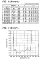
- FIGS. 9 and 10 show the first numerical example (Examples 1-1 and 1-2).
- FIGS. 9(A) and 10(A) show basic data of Examples 1-1 and 1-2 corresponding to the antireflection film C 1 shown in FIG. 1 , respectively.
- FIGS. 9(B) and 10(B) show reflectivity distributions of Examples 1-1 and 1-2, respectively.
- FIGS. 9(A) and 10(A) the constituent material, refractive index N with respect to the d-line, physical thickness d (unit: nm), and optical thickness (unit: nm) of each layer are shown.
- the term “sub-h4” in the column of the constituent material indicates Substance H4 (Merck KGaA, Germany) which consists primarily of LaTiO 3 . All the center wavelengths ⁇ 0 indicated in the column of the optical thickness N ⁇ d are 480 nm.
- the refractive indices N and optical thicknesses N ⁇ d of the layers satisfy all of conditional expressions (1) to (10).
- FIGS. 9(A) and 10(A) the constituent material, refractive index N with respect to the d-line, physical thickness d (unit: nm), and optical thickness (unit: nm) of each layer are shown.
- the term “sub-h4” in the column of the constituent material indicates Substance H4 (Merck KGaA, Germany) which consists
- FIGS. 11 to 18 show the second numerical example (Examples 2-1 to 2-8).
- FIGS. 11(A) , 12 (A), 13 (A), 14 (A), 15 (A), 16 (A), 17 (A), and 18 (A) show basic data of Examples 2-1 to 2-8 corresponding to the antireflection film C 2 shown in FIG. 2 , respectively.
- All the center wavelengths ⁇ 0 indicated in the column of the optical thickness N ⁇ d are 480 nm.
- the tenth layer which is closest to the substrate is configured by Y 2 O 3 , and, in Examples 2-4 to 2-8, configured by Substance H4 (Merck KGaA, Germany).
- the refractive indices N and optical thicknesses N ⁇ d of the layers satisfy all of conditional expressions (1) to (6) and (11) to (14).
- FIGS. 11(B) , 12 (B), 13 (B), 14 (B), 15 (B), 16 (B), 17 (B), and 18 (B) show reflectivity distributions of Examples 2-1 to 2-8, respectively.
- the reflectivities in the wavelength band of about 400 to 700 nm stay within a range from 0.05 to 0.15%.
- FIGS. 19 and 20 show the numerical example (Examples 3-1 and 3-2) corresponding to the antireflection film C 3 shown in FIG. 3 .
- FIGS. 19(A) and 20(A) show basic data of Examples 3-1 and 3-2, respectively. All the center wavelengths ⁇ 0 indicated in the column of the optical thickness N ⁇ d are 480 nm. As seen from the figures, the refractive indices N and optical thicknesses N ⁇ d of the layers satisfy all of conditional expressions (1) to (6) and (15) to (20).
- FIGS. 19(B) and 20(B) show reflectivity distributions of Examples 3-1 and 3-2, respectively. As seen from the figures, the reflectivities in the wavelength band of about 400 to 700 nm stay within a range from 0.05 to 0.15%.
- FIGS. 21 to 24 show the fourth numerical example (Examples 4-1 to 4-4).
- FIGS. 21(A) , 22 (A), 23 (A), and 24 (A) show basic data of Examples 4-1 to 4-4 corresponding to the antireflection film C 4 shown in FIG. 4 , respectively.
- the center wavelengths ⁇ 0 indicated in the column of the optical thickness N ⁇ d are 480 nm, and, in Example 4-4, the center wavelength is 690 nm.
- the refractive indices N and optical thicknesses N ⁇ d of the layers satisfy all of conditional expressions (1) to (6) and (21) to (24).
- FIGS. 21(B) , 22 (B), 23 (B), and 24 (B) show reflectivity distributions of Examples 4-1 to 4-4, respectively.
- the reflectivities in the wavelength band of about 400 to 700 nm are approximately 0.15% or less; and in the Example 4-4, the reflectivities in the wavelength band of about 550 to 1,000 nm are approximately 0.15% or less.
- FIGS. 25 to 32 show the fifth numerical example (Examples 5-1 to 5-8).
- FIGS. 25(A) , 26 (A), 27 (A), 28 (A), 29 (A), 30 (A), 31 (A), and 32 (A) show basic data of Examples 5-1 to 5-8 corresponding to the antireflection film C 5 shown in FIG. 5 , respectively.
- the center wavelengths ⁇ 0 indicated in the column of the optical thickness N ⁇ d are 480 nm, and, in Examples 5-7 and 5-8, the center wavelengths are 690 nm.
- the refractive indices N and optical thicknesses N ⁇ d of the layers satisfy all of conditional expressions (1) to (6) and (25) to (27).
- FIGS. 25(B) , 26 (B), 27 (B), 28 (B), 29 (B), 30 (B), 31 (B), and 32 (B) show reflectivity distributions of Examples 5-1 to 5-8, respectively.
- the reflectivities in the wavelength band of about 400 to 700 nm are approximately 0.15% or less
- the reflectivities in the wavelength band of about 550 to 1,000 nm stay within a range from 0.05 to 0.15%.
- FIGS. 33 to 35 show the sixth numerical example (Examples 6-1 to 6-3).
- FIGS. 33(A) , 34 (A), and 35 (A) show basic data of Examples 6-1 to 6-3 corresponding to the antireflection film C 6 shown in FIG. 6 , respectively. All the center wavelengths ⁇ 0 indicated in the column of the optical thickness N ⁇ d are 480 nm. As seen from the figures, the refractive indices N and optical thicknesses N ⁇ d of the layers satisfy all of conditional expressions (1) to (6), (28), and (29).
- FIGS. 33(B) , 34 (B), and 35 (B) show reflectivity distributions of Examples 6-1 to 6-3, respectively. As seen from the figures, the reflectivities in the wavelength band of about 400 to 700 nm are 0.15% or less.
- FIGS. 36 to 38 show the seventh numerical example (Examples 7-1 to 7-3).
- FIGS. 36(A) , 37 (A), and 38 (A) show basic data of Examples 7-1 to 7-3 corresponding to the antireflection film C 7 shown in FIG. 7 , respectively.
- All the center wavelengths ⁇ 0 indicated in the column of the optical thickness N ⁇ d are 480 nm.
- the refractive indices N and optical thicknesses N ⁇ d of the layers satisfy all of conditional expressions (1) to (6), and (30) to (34).
- FIGS. 36(B) , 37 (B), and 38 (B) show reflectivity distributions of Examples 7-1 to 7-3, respectively. As seen from the figures, the reflectivities in the wavelength band of about 400 to 700 nm are 0.15% or less.
- FIGS. 39 and 40 show the eighth numerical example (Examples 8-1 and 8-2).
- FIGS. 39(A) and 40(A) show basic data of Examples 8-1 and 8-2 corresponding to the antireflection film C 8 shown in FIG. 8 , respectively. All the center wavelengths ⁇ 0 indicated in the column of the optical thickness N ⁇ d are 480 nm. As seen from the figures, the refractive indices N and optical thicknesses N ⁇ d of the layers satisfy all of conditional expressions (1) to (6), and (35) to (39).
- FIGS. 39(B) and 40(B) show reflectivity distributions of Examples 8-1 and 8-2, respectively. As seen from the figures, the reflectivities in the wavelength band of about 400 to 700 nm are 0.15% or less.
- the embodiments exert a very excellent reflectivity distribution. Namely, it was confirmed that the antireflection film of the invention can sufficiently reduce the reflectivity in a predetermined wavelength band, and satisfactorily flatten the distribution of the reflectivity.
- the invention has been described with reference to the embodiments and the examples, the invention is not limited to the embodiments and the examples, and may be variously modified.
- the reflectivities and optical thicknesses of the layers and substrates are not limited to the values shown in the numerical examples, and may have various values.
- the kinds of the materials constituting the layers and the substrates are not limited to those shown in the numerical examples, and other kinds of materials may be used.
- each layer may be configured by plural films on the basis of the equivalent film theory. Namely, two kinds of refractive index films are symmetrically stacked, so that they optically behave as a single layer.
Landscapes
- Physics & Mathematics (AREA)
- General Physics & Mathematics (AREA)
- Optics & Photonics (AREA)
- Chemical & Material Sciences (AREA)
- Inorganic Chemistry (AREA)
- Surface Treatment Of Optical Elements (AREA)
- Laminated Bodies (AREA)
Abstract
Description
0.25×λ0≦N1·d1≦0.27×λ0 (1)
0.48×λ0≦N2·d2≦0.50×λ0 (2)
0.20×λ0≦N3·d3≦0.23×λ0 (3)
0.08×λ0≦N4·d4≦0.09×λ0 (4)
0.27×λ0≦N5·d5≦0.30×λ0 (5)
0.41×λ0≦N6·d6≦0.60×λ0 (6)
where
0.03×λ0≦N7·d7≦0.13×λ0 (7)
0.05×λ0≦N8·d8≦0.11×λ0 (8)
0.08×λ0≦N9·d9≦0.09×λ0 (9)
0.09×λ0≦N10·d10≦0.14×λ0 (10)
where
0.03×λ0≦N7·d7≦0.04×λ0 (11)
0.06×λ0≦N8·d8≦0.11×λ0 (12)
0.08×λ0≦N9·d9≦0.14×λ0 (13)
0.04×λ0≦N10·d10≦0.10×λ0 (14)
where
0.03×λ0≦N7·d7≦0.04×λ0 (15)
0.10×λ0≦N8·d8≦0.12×λ0 (16)
0.10×λ0≦N9·d9≦0.11×λ0 (17)
0.10×λ0≦N10·d10≦0.11×λ0 (18)
0.13×λ0≦N11·d11≦0.16×λ0 (19)
0.04×λ0≦N12·d12≦0.05×λ0 (20)
where
0.08×λ0≦N7·d7≦0.12×λ0 (21)
0.11×λ0≦N8·d8≦0.17×λ0 (22)
0.07×λ0≦N9·d9≦0.18×λ0 (23)
0.04×λ0≦N10·d10≦0.09×λ0 (24)
where
0.08×λ0≦N7·d7≦0.12×λ0 (25)
0.07×λ0≦N8·d8≦0.155×λ0 (26)
0.06×λ0≦N9·d9≦0.12×λ0 (27)
where
0.08×λ0≦N7·d7≦0.11×λ0 (28)
0.05×λ0≦N8·d8≦0.07×λ0 (29)
where
0.04×λ0≦N7·d7≦0.05×λ0 (30)
0.06×λ0≦N8·d8≦0.12×λ0 (31)
0.07×λ0≦N9·d9≦0.12×λ0 (32)
0.05×λ0≦N10·d10≦0.06×λ0 (33)
0.04×λ0≦N11·d11≦0.26×λ0 (34)
where
0.03×λ0≦N7·d7≦0.04×λ0 (35)
0.10×λ0≦N8·d8≦0.12×λ0 (36)
0.11×λ0≦N9·d9≦0.12×λ0 (37)
0.07×λ0≦N10·d10≦0.09×λ0 (38)
0.08×λ0≦N11·d11≦0.09×λ0 (39)
where
0.25×λ0≦N1·d1≦0.27×λ0 (1)
0.48×λ0≦N2·d2≦0.50×λ0 (2)
0.20×λ0≦N3·d3≦0.23×λ0 (3)
0.08×λ0≦N4·d4≦0.09×λ0 (4)
0.27×λ0≦N5·d5≦0.30×λ0 (5)
0.41×λ0≦N6·d6≦0.60×λ0 (6)
0.03×λ0≦N7·d7≦0.13×λ0 (7)
0.05×λ0≦N8·d8≦0.11×λ0 (8)
0.08×λ0≦N9·d9≦0.09×λ0 (9)
0.09×λ0≦N10·d10≦0.14×λ0 (10)
0.03×λ0≦N7·d7≦0.04×λ0 (11)
0.06×λ0≦N8·d8≦0.11×λ0 (12)
0.08×λ0≦N9·d9≦0.14×λ0 (13)
0.04×λ0≦N10·d10≦0.10×λ0 (14)
0.03×λ0≦N7·d7≦0.04×λ0 (15)
0.10×λ0≦N8·d8≦0.12×λ0 (16)
0.10×λ0≦N9·d9≦0.11×λ0 (17)
0.10×λ0≦N10·d10≦0.11×λ0 (18)
0.13×λ0≦N11·d11≦0.16×λ0 (19)
0.04×λ0≦N12·d12≦0.05×λ0 (20)
0.08×λ0≦N7·d7≦0.12×λ0 (21)
0.11×λ0≦N8·d8≦0.17×λ0 (22)
0.07×λ0≦N9·d9≦0.18×λ0 (23)
0.04×λ0≦N10·d10≦0.09×λ0 (24)
0.08×λ0≦N7·d7≦0.12×λ0 (25)
0.07×λ0≦N8·d8≦0.155×λ0 (26)
0.06×λ0≦N9·d9≦0.12×λ0 (27)
0.08×λ0≦N7·d7≦0.11×λ0 (28)
0.05×λ0≦N8·d8≦0.07×λ0 (29)
0.04×λ0≦N7·d7≦0.05×λ0 (30)
0.06×λ0≦N8·d8≦0.12×λ0 (31)
0.07×λ0≦N9·d9≦0.12×λ0 (32)
0.05×λ0≦N10·d10≦0.06×λ0 (33)
0.04×λ0≦N11·d11≦0.26×λ0 (34)
0.03×λ0≦N7·d7≦0.04×λ0 (35)
0.10×λ0≦N8·d8≦0.12×λ0 (36)
0.11×λ0≦N9·d9≦0.12×λ0 (37)
0.07×λ0≦N10·d10≦0.09×λ0 (38)
0.08×λ0≦N11·d11≦0.09×λ0 (39)
Claims (33)
0.25×λ0≦N1·d1≦0.27×λ0 (1)
0.48×λ0≦N2·d2≦0.50×λ0 (2)
0.20×λ0≦N3·d3≦0.23×λ0 (3)
0.08×λ0≦N4·d4≦0.09×λ0 (4)
0.27×λ0≦N5·d5≦0.30×λ0 (5)
0.41×λ0≦N6·d6≦0.60×λ0 (6)
0.03×λ0≦N7·d7≦0.13×λ0 (7)
0.05×λ0≦N8·d8≦0.11×λ0 (8)
0.08×λ0≦N9·d9≦0.09×λ0 (9)
0.09×λ0≦N10·d10≦0.14×λ0 (10)
0.03×λ0≦N7·d7≦0.04×λ0 (11)
0.06×λ0≦N8·d8≦0.11×λ0 (12)
0.08×λ0≦N9·d9≦0.14×λ0 (13)
0.04×λ0≦N10·d10≦0.10×λ0 (14)
0.03×λ0≦N7·d7≦0.04×λ0 (15)
0.10×λ0≦N8·d8≦0.12×λ0 (16)
0.10×λ0≦N9·d9≦0.11×λ0 (17)
0.10×λ0≦N10·d10≦0.11×λ0 (18)
0.13×λ0≦N11·d11≦0.16×λ0 (19)
0.04×λ0≦N12·d12≦0.05×λ0 (20)
0.08×λ0≦N7·d7≦0.12×λ0 (21)
0.11×λ0≦N8·d8≦0.17×λ0 (22)
0.07×λ0≦N9·d9≦0.18×λ0 (23)
0.04×λ0≦N10·d10≦0.09×λ0 (24)
0.08×λ0≦N7·d7≦0.12×λ0 (25)
0.07×λ0≦N8·d8≦0.155×λ0 (26)
0.06×λ0≦N9·d9≦0.12×λ0 (27)
0.08×λ0≦N7·d7≦0.11×λ0 (28)
0.05×λ0≦N8·d8≦0.07×λ0 (29)
0.04×λ0≦N7·d7≦0.05×λ0 (30)
0.06×λ0≦N8·d8≦0.12×λ0 (31)
0.07×λ0≦N9·d9≦0.12×λ0 (32)
0.05×λ0≦N10·d10≦0.06×λ0 (33)
0.04×λ0≦N11·d11≦0.26×λ0 (34)
0.03×λ0≦N7·d7≦0.04×λ0 (35)
0.10×λ0≦N8·d8≦0.12×λ0 (36)
0.11×λ0≦N9·d9≦0.12×λ0 (37)
0.07×λ0≦N10·d10≦0.09×λ0 (38)
0.08×λ0≦N11·d11≦0.09×λ0 (39)
Applications Claiming Priority (4)
| Application Number | Priority Date | Filing Date | Title |
|---|---|---|---|
| JPP2006-005133 | 2006-01-12 | ||
| JP2006005133 | 2006-01-12 | ||
| JP2006345552A JP4958536B2 (en) | 2006-01-12 | 2006-12-22 | Anti-reflection coating |
| JPP2006-345552 | 2006-12-22 |
Publications (2)
| Publication Number | Publication Date |
|---|---|
| US20070159697A1 US20070159697A1 (en) | 2007-07-12 |
| US7773301B2 true US7773301B2 (en) | 2010-08-10 |
Family
ID=37896055
Family Applications (1)
| Application Number | Title | Priority Date | Filing Date |
|---|---|---|---|
| US11/652,021 Expired - Fee Related US7773301B2 (en) | 2006-01-12 | 2007-01-11 | Antireflection film |
Country Status (3)
| Country | Link |
|---|---|
| US (1) | US7773301B2 (en) |
| EP (1) | EP1808714A1 (en) |
| JP (1) | JP4958536B2 (en) |
Cited By (4)
| Publication number | Priority date | Publication date | Assignee | Title |
|---|---|---|---|---|
| US20090303590A1 (en) * | 2008-06-06 | 2009-12-10 | Canon Kabushiki Kaisha | Optical filter and imaging apparatus |
| JP2011257677A (en) * | 2010-06-11 | 2011-12-22 | Konica Minolta Opto Inc | Optical element and method for manufacturing the same |
| US9201172B2 (en) | 2012-09-14 | 2015-12-01 | Ricoh Imaging Company, Ltd. | Anti-reflection coating, optical member having it, and optical equipment comprising such optical member |
| US20160277718A1 (en) * | 2015-03-17 | 2016-09-22 | Konica Minolta, Inc. | Projection lens and projector |
Families Citing this family (33)
| Publication number | Priority date | Publication date | Assignee | Title |
|---|---|---|---|---|
| CA2701672C (en) * | 2007-09-28 | 2017-10-24 | Nikon-Essilor Co., Ltd. | Optical component and method for manufacturing the same |
| EP2128658A3 (en) | 2008-05-22 | 2011-05-11 | Fujinon Corporation | Reflection reducing film, optical member and optical system |
| JP5197274B2 (en) * | 2008-09-26 | 2013-05-15 | 日東光学株式会社 | Optical member manufacturing method and optical member |
| JP5489604B2 (en) * | 2009-01-14 | 2014-05-14 | ホーヤ レンズ マニュファクチャリング フィリピン インク | Method for manufacturing optical article |
| JP2010231172A (en) * | 2009-03-04 | 2010-10-14 | Seiko Epson Corp | Optical article and manufacturing method thereof |
| JP5698902B2 (en) * | 2009-03-04 | 2015-04-08 | ホーヤ レンズ マニュファクチャリング フィリピン インク | Optical article and manufacturing method thereof |
| CN101806927B (en) * | 2010-02-25 | 2013-09-11 | 海洋王照明科技股份有限公司 | High-reflecting film and preparation method thereof |
| JP2012032690A (en) | 2010-08-02 | 2012-02-16 | Seiko Epson Corp | Optical article and manufacturing method thereof |
| JP5768411B2 (en) * | 2011-03-04 | 2015-08-26 | セイコーエプソン株式会社 | Method for producing lanthanum titanate particles |
| JP6202785B2 (en) * | 2012-05-30 | 2017-09-27 | オリンパス株式会社 | Antireflection film, optical system, optical apparatus, and method for forming antireflection film |
| JP6268691B2 (en) * | 2012-08-03 | 2018-01-31 | リコーイメージング株式会社 | Beam splitting optical element and digital single lens reflex camera |
| US9110230B2 (en) | 2013-05-07 | 2015-08-18 | Corning Incorporated | Scratch-resistant articles with retained optical properties |
| ES2536827B1 (en) * | 2013-11-27 | 2015-12-18 | Indo Optical S.L. | Ophthalmic lens comprising a base of polymeric material with a coating with a multilayer anti-reflective, anti-reflective and IR filter multilayer structure |
| JP6385117B2 (en) * | 2014-04-11 | 2018-09-05 | キヤノン株式会社 | Optical element and optical system having the same |
| US11267973B2 (en) | 2014-05-12 | 2022-03-08 | Corning Incorporated | Durable anti-reflective articles |
| KR20150138983A (en) * | 2014-05-30 | 2015-12-11 | 삼성디스플레이 주식회사 | Optical multi-layered unit and display device comprising the same |
| EP3770649A1 (en) * | 2015-09-14 | 2021-01-27 | Corning Incorporated | High light transmission and scratch-resistant anti-reflective articles |
| JP6795031B2 (en) | 2016-05-26 | 2020-12-02 | コニカミノルタ株式会社 | Projection lens |
| CN106291781A (en) * | 2016-08-30 | 2017-01-04 | 东兴华鸿光学科技有限公司 | Optical glass anti-reflection film |
| CN106707376A (en) * | 2016-12-22 | 2017-05-24 | 湖北东田光电材料科技有限公司 | Optical lens film-coated film layer structure and film coating method of optical lens film-coated film layer structure |
| US10754068B2 (en) * | 2018-06-04 | 2020-08-25 | Engineered Outdoor Products, LLC | Lens coating system |
| EP3837223A1 (en) | 2018-08-17 | 2021-06-23 | Corning Incorporated | Inorganic oxide articles with thin, durable anti-reflective structures |
| US11650361B2 (en) | 2018-12-27 | 2023-05-16 | Viavi Solutions Inc. | Optical filter |
| CN109856707B (en) * | 2019-02-26 | 2021-05-04 | 江西凤凰光学科技有限公司 | Antireflection film with broadband and ultralow reflectivity |
| CN110174718B (en) * | 2019-06-28 | 2025-02-28 | 浙江舜宇光学有限公司 | Coated lens and optical imaging device |
| CN112987139A (en) * | 2019-12-13 | 2021-06-18 | 中山火炬职业技术学院 | Multifunctional optical coating goggles lens and preparation method thereof |
| JP7347203B2 (en) * | 2019-12-25 | 2023-09-20 | コニカミノルタ株式会社 | Optical lenses with anti-reflection coating, projection lenses and projection lens optical systems |
| US12147009B2 (en) | 2020-07-09 | 2024-11-19 | Corning Incorporated | Textured region to reduce specular reflectance including a low refractive index substrate with higher elevated surfaces and lower elevated surfaces and a high refractive index material disposed on the lower elevated surfaces |
| JP2022069259A (en) * | 2020-10-23 | 2022-05-11 | 東海光学株式会社 | Plastic optical products and plastic spectacle lenses |
| US20240069249A1 (en) * | 2022-08-31 | 2024-02-29 | Samsung Electro-Mechanics Co., Ltd. | Lens and lens module including lens |
| CN116040965B (en) * | 2023-01-31 | 2024-02-27 | 宁波启朴芯微系统技术有限公司 | Broadband antireflection film and preparation method and application thereof |
| TWI835646B (en) * | 2023-05-10 | 2024-03-11 | 澤米科技股份有限公司 | Optical component structure with a lanthanide compound layer |
| WO2026083763A1 (en) * | 2024-10-17 | 2026-04-23 | 株式会社ニコン・エシロール | Optical article |
Citations (6)
| Publication number | Priority date | Publication date | Assignee | Title |
|---|---|---|---|---|
| US4726654A (en) | 1985-11-25 | 1988-02-23 | Minolta Camera Kabushiki Kaisha | Multi-layered anti-reflection coating |
| JP2001100002A (en) | 1999-09-29 | 2001-04-13 | Canon Inc | Antireflection film and optical member using the same |
| JP2002107506A (en) | 2000-09-28 | 2002-04-10 | Canon Inc | Antireflection film and optical component using the same |
| JP2002267801A (en) | 2001-03-12 | 2002-09-18 | Canon Inc | Antireflection film and optical member using the same |
| US20050122576A1 (en) | 2002-02-26 | 2005-06-09 | Atsushi Yonetani | Anti-reflection film and microscope having optical element with the same anti-reflection film applied thereto |
| US20050201422A1 (en) | 2004-02-16 | 2005-09-15 | Tatsuo Ohta | Optical element and optical pickup apparatus |
Family Cites Families (1)
| Publication number | Priority date | Publication date | Assignee | Title |
|---|---|---|---|---|
| JP4190773B2 (en) * | 2002-02-26 | 2008-12-03 | オリンパス株式会社 | Antireflection film, optical lens and optical lens unit |
-
2006
- 2006-12-22 JP JP2006345552A patent/JP4958536B2/en not_active Expired - Fee Related
-
2007
- 2007-01-10 EP EP07000445A patent/EP1808714A1/en not_active Withdrawn
- 2007-01-11 US US11/652,021 patent/US7773301B2/en not_active Expired - Fee Related
Patent Citations (6)
| Publication number | Priority date | Publication date | Assignee | Title |
|---|---|---|---|---|
| US4726654A (en) | 1985-11-25 | 1988-02-23 | Minolta Camera Kabushiki Kaisha | Multi-layered anti-reflection coating |
| JP2001100002A (en) | 1999-09-29 | 2001-04-13 | Canon Inc | Antireflection film and optical member using the same |
| JP2002107506A (en) | 2000-09-28 | 2002-04-10 | Canon Inc | Antireflection film and optical component using the same |
| JP2002267801A (en) | 2001-03-12 | 2002-09-18 | Canon Inc | Antireflection film and optical member using the same |
| US20050122576A1 (en) | 2002-02-26 | 2005-06-09 | Atsushi Yonetani | Anti-reflection film and microscope having optical element with the same anti-reflection film applied thereto |
| US20050201422A1 (en) | 2004-02-16 | 2005-09-15 | Tatsuo Ohta | Optical element and optical pickup apparatus |
Non-Patent Citations (4)
| Title |
|---|
| "What's new in Optilayer in 2008 (major updates, version 7.21)", Optilayer Thin Film Software, retrieved from the Internet on Jun. 8, 2009: http://www.optilayer.com/whats-new.htm>. |
| Liou, Japanese Journal of Applied Physics, "Designing a Broadband Visible Antireflection Coating by Flip-Flop Tuning Search Technique," vol. 42, No. 11, pp. 6879-6882, (Nov. 10, 2003) XP002428367. |
| Office Action, dated Jun. 15, 2009, for corresponding European Application No. 07000445.2. |
| Tikhonravov et al., Applied Optics, "Application of the Needle Optimization Technique to the Design of Optical Coatings," vol. 35, No. 28, pp. 5493-5508, (Oct. 1, 1996) XP009053835. |
Cited By (5)
| Publication number | Priority date | Publication date | Assignee | Title |
|---|---|---|---|---|
| US20090303590A1 (en) * | 2008-06-06 | 2009-12-10 | Canon Kabushiki Kaisha | Optical filter and imaging apparatus |
| JP2011257677A (en) * | 2010-06-11 | 2011-12-22 | Konica Minolta Opto Inc | Optical element and method for manufacturing the same |
| US9201172B2 (en) | 2012-09-14 | 2015-12-01 | Ricoh Imaging Company, Ltd. | Anti-reflection coating, optical member having it, and optical equipment comprising such optical member |
| US20160277718A1 (en) * | 2015-03-17 | 2016-09-22 | Konica Minolta, Inc. | Projection lens and projector |
| US10145988B2 (en) * | 2015-03-17 | 2018-12-04 | Konica Minolta, Inc. | Projection lens and projector with laser beam light source |
Also Published As
| Publication number | Publication date |
|---|---|
| US20070159697A1 (en) | 2007-07-12 |
| JP4958536B2 (en) | 2012-06-20 |
| EP1808714A1 (en) | 2007-07-18 |
| JP2007213021A (en) | 2007-08-23 |
Similar Documents
| Publication | Publication Date | Title |
|---|---|---|
| US7773301B2 (en) | Antireflection film | |
| JP4958594B2 (en) | Antireflection film, optical element and optical system | |
| EP2708922B1 (en) | Anti-reflection coating, optical member having it, and optical equipment comprising such optical member | |
| JP4630915B2 (en) | Antireflection film, optical member, optical system | |
| JP6051710B2 (en) | Antireflection film, optical member using the same, and optical instrument | |
| US8248699B2 (en) | Reflection reducing film, optical member and optical system | |
| US3799653A (en) | Multi-layer anti-reflection coating | |
| CN101105547A (en) | Dielectric multilayer filter | |
| WO2009133833A1 (en) | Optical device and antireflection film | |
| JP6241102B2 (en) | Antireflection film, optical member using the same, and optical instrument | |
| CN113031122B (en) | Optical lens with antireflection film, projection lens, and projection lens optical system | |
| WO2018216310A1 (en) | Optical element and projection lens | |
| JP4630916B2 (en) | Antireflection film, optical member, optical system | |
| JP2007333806A (en) | Antireflection film and optical member | |
| JP2001100002A (en) | Antireflection film and optical member using the same | |
| JP6236776B2 (en) | Antireflection film, optical member using the same, and optical instrument | |
| JP6361095B2 (en) | Antireflection film, optical member using the same, and optical instrument | |
| JP2017040946A (en) | Antireflection film, optical member using the same, and optical apparatus | |
| JP2024157359A (en) | Optical system and imaging device including the same | |
| JP2005055569A (en) | Antireflection film |
Legal Events
| Date | Code | Title | Description |
|---|---|---|---|
| AS | Assignment |
Owner name: FUJINON CORPORATION, JAPAN Free format text: ASSIGNMENT OF ASSIGNORS INTEREST;ASSIGNOR:TERAYAMA, ETSUO;REEL/FRAME:018801/0336 Effective date: 20061228 |
|
| FEPP | Fee payment procedure |
Free format text: PAYOR NUMBER ASSIGNED (ORIGINAL EVENT CODE: ASPN); ENTITY STATUS OF PATENT OWNER: LARGE ENTITY |
|
| REMI | Maintenance fee reminder mailed | ||
| LAPS | Lapse for failure to pay maintenance fees | ||
| STCH | Information on status: patent discontinuation |
Free format text: PATENT EXPIRED DUE TO NONPAYMENT OF MAINTENANCE FEES UNDER 37 CFR 1.362 |
|
| STCH | Information on status: patent discontinuation |
Free format text: PATENT EXPIRED DUE TO NONPAYMENT OF MAINTENANCE FEES UNDER 37 CFR 1.362 |
|
| FP | Lapsed due to failure to pay maintenance fee |
Effective date: 20140810 |