US7771614B2 - Low power bistable device and method - Google Patents
Low power bistable device and method Download PDFInfo
- Publication number
- US7771614B2 US7771614B2 US11/945,230 US94523007A US7771614B2 US 7771614 B2 US7771614 B2 US 7771614B2 US 94523007 A US94523007 A US 94523007A US 7771614 B2 US7771614 B2 US 7771614B2
- Authority
- US
- United States
- Prior art keywords
- liquid crystal
- crystal material
- display device
- display
- crystal molecules
- Prior art date
- Legal status (The legal status is an assumption and is not a legal conclusion. Google has not performed a legal analysis and makes no representation as to the accuracy of the status listed.)
- Expired - Fee Related
Links
Images


Classifications
-
- C—CHEMISTRY; METALLURGY
- C09—DYES; PAINTS; POLISHES; NATURAL RESINS; ADHESIVES; COMPOSITIONS NOT OTHERWISE PROVIDED FOR; APPLICATIONS OF MATERIALS NOT OTHERWISE PROVIDED FOR
- C09K—MATERIALS FOR MISCELLANEOUS APPLICATIONS, NOT PROVIDED FOR ELSEWHERE
- C09K19/00—Liquid crystal materials
- C09K19/52—Liquid crystal materials characterised by components which are not liquid crystals, e.g. additives with special physical aspect: solvents, solid particles
- C09K19/58—Dopants or charge transfer agents
- C09K19/586—Optically active dopants; chiral dopants
-
- C—CHEMISTRY; METALLURGY
- C09—DYES; PAINTS; POLISHES; NATURAL RESINS; ADHESIVES; COMPOSITIONS NOT OTHERWISE PROVIDED FOR; APPLICATIONS OF MATERIALS NOT OTHERWISE PROVIDED FOR
- C09K—MATERIALS FOR MISCELLANEOUS APPLICATIONS, NOT PROVIDED FOR ELSEWHERE
- C09K19/00—Liquid crystal materials
- C09K19/52—Liquid crystal materials characterised by components which are not liquid crystals, e.g. additives with special physical aspect: solvents, solid particles
- C09K19/58—Dopants or charge transfer agents
-
- G—PHYSICS
- G02—OPTICS
- G02F—OPTICAL DEVICES OR ARRANGEMENTS FOR THE CONTROL OF LIGHT BY MODIFICATION OF THE OPTICAL PROPERTIES OF THE MEDIA OF THE ELEMENTS INVOLVED THEREIN; NON-LINEAR OPTICS; FREQUENCY-CHANGING OF LIGHT; OPTICAL LOGIC ELEMENTS; OPTICAL ANALOGUE/DIGITAL CONVERTERS
- G02F1/00—Devices or arrangements for the control of the intensity, colour, phase, polarisation or direction of light arriving from an independent light source, e.g. switching, gating or modulating; Non-linear optics
- G02F1/01—Devices or arrangements for the control of the intensity, colour, phase, polarisation or direction of light arriving from an independent light source, e.g. switching, gating or modulating; Non-linear optics for the control of the intensity, phase, polarisation or colour
- G02F1/13—Devices or arrangements for the control of the intensity, colour, phase, polarisation or direction of light arriving from an independent light source, e.g. switching, gating or modulating; Non-linear optics for the control of the intensity, phase, polarisation or colour based on liquid crystals, e.g. single liquid crystal display cells
- G02F1/137—Devices or arrangements for the control of the intensity, colour, phase, polarisation or direction of light arriving from an independent light source, e.g. switching, gating or modulating; Non-linear optics for the control of the intensity, phase, polarisation or colour based on liquid crystals, e.g. single liquid crystal display cells characterised by the electro-optical or magneto-optical effect, e.g. field-induced phase transition, orientation effect, guest-host interaction or dynamic scattering
- G02F1/13718—Devices or arrangements for the control of the intensity, colour, phase, polarisation or direction of light arriving from an independent light source, e.g. switching, gating or modulating; Non-linear optics for the control of the intensity, phase, polarisation or colour based on liquid crystals, e.g. single liquid crystal display cells characterised by the electro-optical or magneto-optical effect, e.g. field-induced phase transition, orientation effect, guest-host interaction or dynamic scattering based on a change of the texture state of a cholesteric liquid crystal
-
- C—CHEMISTRY; METALLURGY
- C09—DYES; PAINTS; POLISHES; NATURAL RESINS; ADHESIVES; COMPOSITIONS NOT OTHERWISE PROVIDED FOR; APPLICATIONS OF MATERIALS NOT OTHERWISE PROVIDED FOR
- C09K—MATERIALS FOR MISCELLANEOUS APPLICATIONS, NOT PROVIDED FOR ELSEWHERE
- C09K2323/00—Functional layers of liquid crystal optical display excluding electroactive liquid crystal layer characterised by chemical composition
- C09K2323/03—Viewing layer characterised by chemical composition
Definitions
- a display device and in particular a low power bistable display device and method are disclosed.
- a display device typically has an ON state and an OFF state wherein the display device is able to display information only when power is being continuously applied to the display device. For example, most televisions operate in this manner. Thus, these display devices have a single stable state in which the state of the display device is maintained without additional power being applied to the display device and the single stable state in the OFF state. The ON state is thus unstable since the ON state is only maintained by applying power to the display device. These typical display devices consume a significant amount of power since power must be applied to the display device to display an image or text.
- Bistable display devices also exist that can, to some extent, maintain the ON state (and continue to display images/text) with reduced power consumption or no power consumption for an amount of time.
- the OFF state and the ON state are stable states because both states can be maintained without the application of a significant amount of additional power.
- bistable displays such as the electrophoretic displays, electrochromic displays, electrowetting displays, MEMS displays, and LCD displays.
- bistable LCD displays there are a few types including nematic types (ZBD and BiNem); cholesteric types (BCD and PDChLC) and smectic types (SSFLC and Smectic-A LCD).
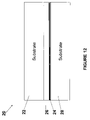
- FIG. 1 illustrates an example of the structure of a liquid crystal display 10 .
- the display 10 has a first and second substrate 12 , 14 (which typically may be made of glass) that contain and sandwich liquid crystal material 16 .
- One or more of the substrates may also contain an electrode (often made of indium tin oxide since it is transparent to visible light) that provides power to the display and induces an electric field that is used to control the liquid crystal material and therefore display information.
- the display 10 may also have a layer 18 that absorbs light that passes through the liquid crystal in the ON state and produces a better black state in which the display is displaying information.
- a cholesteric type liquid crystal is one of three major liquid crystal phases.
- the planar texture and the focal-conic texture are two stable textures.
- the liquid crystal molecules are basically aligned to be parallel to the substrates.
- the helical axes of the cholesterics are perpendicular to the substrates.
- the focal-conic texture the helical axes of many cholesteric liquid crystal domains are randomly oriented with no preferred direction.
- cholesteric type liquid crystal display is a positive cholesteric bistable display.
- a high voltage is able to unwind the helix of cholesteric liquid crystal and turns them into a homeotropic state to orient along the electric field. Releasing the field, the liquid crystal will relax into either the planar texture or the focal conic texture, depending on how the post-field is applied. At a low post-voltage, the liquid crystal will end up at the focal conic texture. If the post-voltage is relatively high, the planar texture will be reached. In this device, both surfaces are homogeneously aligned but usually with no preferred azimuthal orientations.
- the cholesteric liquid crystal may be tuned by the chiral dopants to have a particular intrinsic reflective spectra within the visible band.
- a colored light is reflected back due to the so-called Bragg-like scattering.
- the incident light basically passes through the thin layer liquid crystal to reach aback layer behind the glass and hence the device takes on the color of that layer in that region.
- PENChLC polymer-enhanced negative cholesteric liquid crystal
- PENChLC utilizes polymer networks to establish bistability in negative cholesteric based displays.
- the ionic compounds are intentionally blended in the host liquid crystal solution to increase its conductivity.
- the polymer networks are built inside the liquid crystals to confine the mobility of liquid crystal molecules in order to establish the long term bistability. While these devices provide long term bistability, they are more difficult to manufacture and more expensive since the polymer network has to be added into the liquid crystal material.
- liquid crystal device fabrication lines prefer to not manufacture these devices with the polymer network since adding the polymer network is messy and introduces additional step(s) into the fabrication process so that the fabrication lines charge a premium to manufacture these devices which further increases the cost of the polymer network LCDs.
- FIG. 1 is a cut-away side view of a liquid crystal display device
- FIGS. 2A and 2B illustrate two states of a low power bistable display
- FIGS. 3A and 3B illustrate a planar texture and a focal conic texture of the low power bistable display
- FIGS. 4-15 illustrate other embodiments of the low power, bistable display.
- the low power bistable display is particularly applicable to a cholesteric LCD which is a non polymer based bistable negative cholesteric display for low power image or text display applications and it is in this context that the low power, bistable display will be described. It will be appreciated, however, that the low power, bistable display has greater utility since it can be manufactured in other manners than those described below (as long as the display has the properties of the low power bistable display described below) and can be used for applications other than the low power image display applications described below and in particular can be used in any application in which it is desirable to have a display that has the ability to display an image, text, etc for long periods of time with minimal power consumption.
- FIGS. 2A and 2B illustrate two states of a low power bistable display 20 and FIGS. 3A and 3B illustrate a planar texture and a focal conic texture of the low power bistable display 20 .
- the display 20 may have a top substrate 22 , an optional alignment layer 24 (that may be on either the top substrate, bottom substrate or both) and liquid crystal material 26 sandwiched between the top substrate 22 and a bottom substrate 28 .
- the display may also have one or more optical film layers (not shown) that will be shown and described below in more detail.
- a set of one or more electrodes made of a material transparent to light, such as indium tin oxide (ITO), may be formed on the top or bottom substrate or optionally material not transparent to light on the bottom and may generate an electric field across particular portions of the liquid crystal material (defining a set of independently controllable pixels or segments of the liquid crystal material) to control the state of the liquid crystal material at particular areas of the display which allows the display to show text, numerals, images, etc, on the display.
- FIG. 2A shows a transmissive state of the low power display device (planar state) with the liquid crystal molecules parallel to the substrates) while FIG.
- the display device 20 may also have a drive circuit (not shown) and a power supply, such as a battery, that supplies power to the electrodes to control the operation of the display device.
- the liquid crystal material 26 may be a negative cholesteric liquid crystal material.
- a certain first frequency electric field is chosen such that when applied the negative dielectric anisotropy of the liquid crystals makes the liquid crystal molecules align perpendicular to the electric field so that the liquid crystals are forced to form the planar texture as shown in FIG. 2A .
- a certain second frequency field is chosen such that when it is applied, the liquid crystal molecules are forced into the focal conic state.
- the first frequency may be between 0.000001 MHz and 0.0005 MHz and in one embodiment, the first frequency is less than 0.0001 MHz with the voltage varied between 0V and 50V.
- the second frequency may be between 0.0005 MHz and 0.01 MHz and in one embodiment, the second frequency is less than 0.001 MHz and the voltage is varied between 0V and 50V.
- the focal conic texture is established as shown in FIGS. 2B and 3B .
- the low power, bistable display has long term bistability without the presence of the field.
- the liquid crystal material in some embodiments, may also include glass beads, polymeric microfibers, polymeric microspheres, spacer beads and/or sticky glass beads, or other spacer methods which are and can be commonly used in the construction of LCD devices.
- the alignment layers 24 may be one or more specially treated substrate surface(s) that impose the homeotropic alignment and the display 20 may include a backing material, that may be laminated on the back of the bottom substrate, to modify and enhance back reflection and refraction properties to form a low power bistable display with long term bistability.
- the homeotropic alignment is built on either or both substrates by depositing a polymer layer or by other means. By utilizing the bonding or coupling affinity between the liquid crystal material mixture and the alignment layer, the quality of each state and the bistability are much enhanced and promoted by this homeotropic alignment layer.
- a variety of surface treatments or lack thereof, can be used on either or both substrates for this and may include, but are not limited to either homeotropic or homogeneous alignment.
- Various materials including a for example, a polyimide can be coated on the surface of one or both substrate(s), and then cured, followed with or without mechanical action to form such homeotropic alignment.
- the low power bistable display uses the negative dielectric anisotropy of the negative liquid crystal.
- the low power bistable display has a transmissive state (as shown in FIG. 2A or 3 A) and a reflective state (as shown in FIG. 2B or 3 B).
- a certain frequency electric field is chosen such that when applied, the negative dielectric anisotropy of the liquid crystals makes the liquid crystal molecules align to be perpendicular to the electric field so that the liquid crystals are forced to form the planar texture as shown in FIGS. 2A and 3A .
- the liquid crystal molecules with the chiral and/or ionic doping have the characteristic that they allow visible incident light 32 to pass through the liquid crystal material.
- the cholesteric liquid crystal is doped by the chiral compounds so that the planar texture of the liquid crystals (shown in FIGS. 2A and 3A ) are usable as a first optical state of the low power, bistable display device.
- the area will be transparent and may take on the appearance of a material behind the display in that area wherein the material may be dark, bright, colored or varied.
- the electric field is relaxed (power being removed from the electrodes so an electric field is no longer being applied to the liquid crystal material), the planar texture will be kept for a long term so that any information displayed will be retained for a long period of time.
- the liquid crystal mixtures with the negative dielectric anisotropy and high birefringence are desirable in the low power, bistable display device.
- the molecules of the liquid crystal material In the reflective state as shown in FIG. 2B (also known as the focal conic texture as shown in FIG. 3B ) of the low power, bistable display, the molecules of the liquid crystal material have domains of the helical axes of the molecules of the liquid crystal material pointing randomly at various directions which is represented by the molecules shown in FIGS. 2B and 3B .
- the display may also include a back optical film layer (not shown) that further modulates the backscatter reflection.
- the low power, bistable display may have a number of different configurations and the thickness of the liquid crystal material sandwiched between two substrates may be such that the balance between good optical contrast and the electronic driving voltage is achieved.
- the thickness of the LCD material may range from 2 um to 30 um although other thicknesses also may be used.
- several sandwich structures can be created composed of either hard or flexible substrates whether or not treated by a polyimide and then separated by liquid crystal mixture as described in more detail below.
- FIGS. 4-15 illustrate other embodiments of the low power, bistable display 20 .
- the display 20 in this embodiment includes the top and bottom substrates 22 , 28 , the liquid crystal material 26 with an alignment layer 24 , an optical modulation layer 34 and a film layer 36 that may be black or a color film.
- the optical modulation layer may be plastic, glass or another material of various surface types.
- An example of the optical enhancement layer is a typical lightweight plastic diffuser.
- the film layer 36 may enhance the contrast of the dark, black or color state of the transmissive state of the display device.
- FIG. 4 the display 20 in this embodiment includes the top and bottom substrates 22 , 28 , the liquid crystal material 26 with an alignment layer 24 , an optical modulation layer 34 and a film layer 36 that may be black or a color film.
- the optical modulation layer may be plastic, glass or another material of various surface types.
- An example of the optical enhancement layer is a typical lightweight plastic diffuser.
- the film layer 36 may enhance the contrast of the dark, black or
- the display 20 may include the top and bottom substrates 22 , 28 , the liquid crystal material 26 with an alignment layer 24 on the bottom substrate, the optical enhancement layer 34 and the film layer 36 that may be black or a color film.
- the display 20 may include the top and bottom substrates 22 , 28 , the liquid crystal material 26 with an alignment layer 24 on each of the top and bottom substrates, the optical enhancement layer 34 and the film layer 36 that may be black or a color film.
- the display 20 may include the top and bottom substrates 22 , 28 , the liquid crystal material 26 with an alignment layer 24 on the top substrate, the optical enhancement layer 34 and the film layer 36 that may be black or a color film.
- FIG. 5 the display 20 may include the top and bottom substrates 22 , 28 , the liquid crystal material 26 with an alignment layer 24 on each of the top and bottom substrates, the optical enhancement layer 34 and the film layer 36 that may be black or a color film.
- the display 20 may include the top and bottom substrates 22 , 28 , the liquid crystal material 26 with an alignment
- the display 20 may include the top and bottom substrates 22 , 28 , the liquid crystal material 26 , the optical enhancement layer 34 and the film layer 36 that may be black or a color film.
- the display 20 may include the top and bottom substrates 22 , 28 , the liquid crystal material 26 with the alignment layer 24 on the bottom substrate and the film layer 36 that may be black or a color film.
- the display 20 may include the top and bottom substrates 22 , 28 , the liquid crystal material 26 with the alignment layer 24 on both the top and bottom substrates, and the film layer 36 that may be black or a color film.
- the display 20 may include the top and bottom substrates 22 , 28 , the liquid crystal material 26 with the alignment layer 24 on the top substrate and the film layer 36 that may be black or a color film.
- the display 20 may include the top and bottom substrates 22 , 28 , the liquid crystal material 26 , and the film layer 36 that may be black or a color film.
- FIG. 10 the display 20 may include the top and bottom substrates 22 , 28 , the liquid crystal material 26 with the alignment layer 24 on the top substrate and the film layer 36 that may be black or a color film.
- the display 20 may include the top and bottom substrates 22 , 28 , the liquid crystal material 26 , and the film layer 36 that may be black or a color film.
- the display 20 may include the top bottom substrates 22 , 28 and the liquid crystal material 26 with the alignment layer 24 on the bottom substrate.
- the display 20 may include the top and bottom substrates 22 , 28 and the liquid crystal material 26 with the alignment layer 24 on the top and bottom substrates.
- the display 20 may include the top and bottom substrates 22 , 28 and the liquid crystal material 26 with the alignment layer 24 on the top substrate.
- the display 20 may include the top and bottom substrates 22 , 28 and the liquid crystal material 26 .
- the display device takes on the look of frosted glass with text or image on the frosted glass.
Abstract
Description
Claims (23)
Priority Applications (2)
| Application Number | Priority Date | Filing Date | Title |
|---|---|---|---|
| US11/945,230 US7771614B2 (en) | 2007-11-26 | 2007-11-26 | Low power bistable device and method |
| PCT/US2008/084748 WO2009070613A1 (en) | 2007-11-26 | 2008-11-25 | Low power bistable device and method |
Applications Claiming Priority (1)
| Application Number | Priority Date | Filing Date | Title |
|---|---|---|---|
| US11/945,230 US7771614B2 (en) | 2007-11-26 | 2007-11-26 | Low power bistable device and method |
Publications (2)
| Publication Number | Publication Date |
|---|---|
| US20090136688A1 US20090136688A1 (en) | 2009-05-28 |
| US7771614B2 true US7771614B2 (en) | 2010-08-10 |
Family
ID=40669958
Family Applications (1)
| Application Number | Title | Priority Date | Filing Date |
|---|---|---|---|
| US11/945,230 Expired - Fee Related US7771614B2 (en) | 2007-11-26 | 2007-11-26 | Low power bistable device and method |
Country Status (2)
| Country | Link |
|---|---|
| US (1) | US7771614B2 (en) |
| WO (1) | WO2009070613A1 (en) |
Cited By (1)
| Publication number | Priority date | Publication date | Assignee | Title |
|---|---|---|---|---|
| CN111117409A (en) * | 2019-12-31 | 2020-05-08 | 苏州艾科迪新材料科技有限公司 | Colorful polymer coating and preparation method thereof |
Families Citing this family (8)
| Publication number | Priority date | Publication date | Assignee | Title |
|---|---|---|---|---|
| TWI436313B (en) * | 2008-05-22 | 2014-05-01 | Creator Technology Bv | A stacked display with a bended substrate, an electronic apparatus and a method for manufacturing the same |
| TW201145230A (en) * | 2010-06-02 | 2011-12-16 | Prime View Int Co Ltd | Electronic reading device |
| US9235102B2 (en) * | 2010-08-20 | 2016-01-12 | Idea Zoo, Inc. | Apparatus to manipulate colloidal particles in a bistable medium |
| US10429968B2 (en) * | 2014-11-06 | 2019-10-01 | Visteon Global Technologies, Inc. | Reconfigurable messaging assembly |
| JP6152399B2 (en) * | 2015-04-01 | 2017-06-21 | 国立中央大学 | High contrast bistable scattering type liquid crystal light valve |
| CN109031738A (en) * | 2017-06-12 | 2018-12-18 | 江苏和成显示科技有限公司 | A kind of liquid crystal display device and its application |
| US11493809B2 (en) * | 2021-01-14 | 2022-11-08 | Tpk Advanced Solutions Inc. | Electronic curtain and electronic device |
| CN113391493A (en) * | 2021-07-07 | 2021-09-14 | 南京邮电大学 | Wide-viewing-angle bistable liquid crystal erasable display device and display method thereof |
Citations (3)
| Publication number | Priority date | Publication date | Assignee | Title |
|---|---|---|---|---|
| US6963435B2 (en) * | 2002-03-27 | 2005-11-08 | Avery Dennison Corporation | Switchable electro-optical laminates |
| US20060027784A1 (en) | 2002-12-07 | 2006-02-09 | Matthew Francis | Liquid crystal medium and liquid crystal display with a highly twisted structure |
| US20070200093A1 (en) | 2002-01-10 | 2007-08-30 | West John L | Non-synthetic method for modifying properties of liquid crystals |
Family Cites Families (2)
| Publication number | Priority date | Publication date | Assignee | Title |
|---|---|---|---|---|
| US200093A (en) * | 1878-02-05 | Improvement in traps for drains, sewers | ||
| US27784A (en) * | 1860-04-10 | Fastening foe ax-handles |
-
2007
- 2007-11-26 US US11/945,230 patent/US7771614B2/en not_active Expired - Fee Related
-
2008
- 2008-11-25 WO PCT/US2008/084748 patent/WO2009070613A1/en active Application Filing
Patent Citations (4)
| Publication number | Priority date | Publication date | Assignee | Title |
|---|---|---|---|---|
| US20070200093A1 (en) | 2002-01-10 | 2007-08-30 | West John L | Non-synthetic method for modifying properties of liquid crystals |
| US6963435B2 (en) * | 2002-03-27 | 2005-11-08 | Avery Dennison Corporation | Switchable electro-optical laminates |
| US7023600B2 (en) * | 2002-03-27 | 2006-04-04 | Avery Dennison Corporation | Switchable electro-optical laminates |
| US20060027784A1 (en) | 2002-12-07 | 2006-02-09 | Matthew Francis | Liquid crystal medium and liquid crystal display with a highly twisted structure |
Non-Patent Citations (2)
| Title |
|---|
| PCT/US2008/84748 International Search Report dated Jan. 15, 2009. |
| PCT/US2008/84748 Written Opinion dated Jan. 15, 2009. |
Cited By (1)
| Publication number | Priority date | Publication date | Assignee | Title |
|---|---|---|---|---|
| CN111117409A (en) * | 2019-12-31 | 2020-05-08 | 苏州艾科迪新材料科技有限公司 | Colorful polymer coating and preparation method thereof |
Also Published As
| Publication number | Publication date |
|---|---|
| WO2009070613A1 (en) | 2009-06-04 |
| US20090136688A1 (en) | 2009-05-28 |
Similar Documents
| Publication | Publication Date | Title |
|---|---|---|
| US7771614B2 (en) | Low power bistable device and method | |
| JPH11279558A (en) | Liquid crystal composition of polymer dispersion type and liquid crystal display device containing the same | |
| US6697131B2 (en) | Stacked type reflection liquid crystal display and method for producing the same | |
| US20020180914A1 (en) | Reverse transmittance mode direct-view liquid crystal display employing a liquid crystal having a characteristic wavelength in the non-visible spectrum | |
| KR20000053405A (en) | Reflective liquid crystal display element | |
| US20090190077A1 (en) | Bistable SmA liquid-crystal display | |
| US6271905B1 (en) | Reflective liquid crystal display device | |
| JP4968262B2 (en) | Liquid crystal display element and electronic paper using the same | |
| US8203688B2 (en) | Liquid crystal display | |
| US5790217A (en) | Polymer-dispersed ferroelectric liquid crystal display | |
| US6404471B1 (en) | Reflection liquid crystal display | |
| US5604616A (en) | Dual function electro-optical display device exhibiting a bistable image or a fugitive image depending the applied voltage | |
| US6646710B2 (en) | Light modulator | |
| KR101137864B1 (en) | Liquid Crystal Display Device | |
| EP1059557A1 (en) | Liquid-crystal display | |
| KR100235168B1 (en) | Reflection type lcd device | |
| JP3758634B2 (en) | Liquid crystal display element | |
| CN110161736A (en) | A kind of uneven potential negative liquid crystal transflection display | |
| JP2003029265A (en) | Liquid crystal panel, manufacturing method therefor and liquid crystal display | |
| CN107797327B (en) | LCD (liquid crystal display) | |
| US8330908B2 (en) | Transflective display and fabrication method thereof | |
| JP2002202526A (en) | Liquid crystal display element | |
| JPH06110068A (en) | Liquid crystal display device | |
| Mitrokhin et al. | 62.3: Reflective Bistable Smectic‐A Passive Matrix LCDs | |
| EP0775933A2 (en) | A display device |
Legal Events
| Date | Code | Title | Description |
|---|---|---|---|
| AS | Assignment |
Owner name: ALTIERRE CORPORATION, CALIFORNIA Free format text: ASSIGNMENT OF ASSIGNORS INTEREST;ASSIGNORS:WANG, XIN-JIU;SAXENA, SUNIT;REEL/FRAME:020697/0266 Effective date: 20080314 |
|
| AS | Assignment |
Owner name: VENTURE LENDING & LEASING IV, INC., CALIFORNIA Free format text: SECURITY INTEREST;ASSIGNOR:ALTIERRE CORPORATION;REEL/FRAME:020955/0543 Effective date: 20080505 Owner name: VENTURE LENDING & LEASING IV, INC.,CALIFORNIA Free format text: SECURITY INTEREST;ASSIGNOR:ALTIERRE CORPORATION;REEL/FRAME:020955/0543 Effective date: 20080505 |
|
| AS | Assignment |
Owner name: VENTURE LENDING & LEASING IV, INC.,CALIFORNIA Free format text: RELEASE BY SECURED PARTY;ASSIGNOR:ALTIERRE CORPORATION;REEL/FRAME:021861/0825 Effective date: 20081002 Owner name: VENTURE LENDING & LEASING IV, INC., CALIFORNIA Free format text: RELEASE BY SECURED PARTY;ASSIGNOR:ALTIERRE CORPORATION;REEL/FRAME:021861/0825 Effective date: 20081002 |
|
| STCF | Information on status: patent grant |
Free format text: PATENTED CASE |
|
| FPAY | Fee payment |
Year of fee payment: 4 |
|
| AS | Assignment |
Owner name: WHITE OAK GLOBAL ADVISORS, LLC, CALIFORNIA Free format text: SECURITY INTEREST;ASSIGNOR:ALTIERRE CORPORATION;REEL/FRAME:033254/0466 Effective date: 20140605 |
|
| AS | Assignment |
Owner name: TRINITY CAPITAL FUND III, L.P., ARIZONA Free format text: INTELLECTUAL PROPERTY SECURITY AGREEMENT;ASSIGNOR:ALTIERRE CORPORATION;REEL/FRAME:041226/0204 Effective date: 20161230 Owner name: ALTIERRE CORPORATION, CALIFORNIA Free format text: RELEASE OF SECURITY INTEREST IN INTELLECTUAL PROPERTY (RELEASES RF 33254/0466);ASSIGNOR:WHITE OAK GLOBAL ADVISORS, LLC;REEL/FRAME:041226/0239 Effective date: 20161230 |
|
| MAFP | Maintenance fee payment |
Free format text: PAYMENT OF MAINTENANCE FEE, 8TH YR, SMALL ENTITY (ORIGINAL EVENT CODE: M2552) Year of fee payment: 8 |
|
| AS | Assignment |
Owner name: WESTERN ALLIANCE BANK, CALIFORNIA Free format text: SECURITY INTEREST;ASSIGNOR:ALTIERRE CORPORATION;REEL/FRAME:046470/0641 Effective date: 20180718 |
|
| AS | Assignment |
Owner name: ALTIERRE CORPORATION, CALIFORNIA Free format text: RELEASE BY SECURED PARTY;ASSIGNOR:WESTERN ALLIANCE BANK;REEL/FRAME:052224/0589 Effective date: 20200325 |
|
| FEPP | Fee payment procedure |
Free format text: MAINTENANCE FEE REMINDER MAILED (ORIGINAL EVENT CODE: REM.); ENTITY STATUS OF PATENT OWNER: SMALL ENTITY |
|
| AS | Assignment |
Owner name: STORE INTELLIGENCE, INC., CALIFORNIA Free format text: ASSIGNMENT OF ASSIGNORS INTEREST;ASSIGNOR:TRINITY FUNDING 1, LLC;REEL/FRAME:060504/0927 Effective date: 20200502 Owner name: TRINITY FUNDING 1, LLC, DELAWARE Free format text: ASSIGNMENT OF ASSIGNORS INTEREST;ASSIGNOR:ALTIERRE CORPORATION;REEL/FRAME:060504/0885 Effective date: 20200502 |
|
| LAPS | Lapse for failure to pay maintenance fees |
Free format text: PATENT EXPIRED FOR FAILURE TO PAY MAINTENANCE FEES (ORIGINAL EVENT CODE: EXP.); ENTITY STATUS OF PATENT OWNER: SMALL ENTITY |
|
| STCH | Information on status: patent discontinuation |
Free format text: PATENT EXPIRED DUE TO NONPAYMENT OF MAINTENANCE FEES UNDER 37 CFR 1.362 |
|
| FP | Lapsed due to failure to pay maintenance fee |
Effective date: 20220810 |
|
| AS | Assignment |
Owner name: AGILE DISPLAYS LLC, CALIFORNIA Free format text: ASSIGNMENT OF ASSIGNORS INTEREST;ASSIGNOR:STORE INTELLIGENCE, INC.;REEL/FRAME:061867/0103 Effective date: 20220801 |