US7764552B2 - Semiconductor integrated circuit - Google Patents
Semiconductor integrated circuit Download PDFInfo
- Publication number
- US7764552B2 US7764552B2 US12/085,158 US8515806A US7764552B2 US 7764552 B2 US7764552 B2 US 7764552B2 US 8515806 A US8515806 A US 8515806A US 7764552 B2 US7764552 B2 US 7764552B2
- Authority
- US
- United States
- Prior art keywords
- voltage
- switch
- time
- semiconductor integrated
- decoder
- Prior art date
- Legal status (The legal status is an assumption and is not a legal conclusion. Google has not performed a legal analysis and makes no representation as to the accuracy of the status listed.)
- Active, expires
Links
- 239000004065 semiconductor Substances 0.000 title claims abstract description 81
- 230000004913 activation Effects 0.000 claims description 61
- 230000006870 function Effects 0.000 claims description 53
- 230000004044 response Effects 0.000 claims description 15
- 230000009849 deactivation Effects 0.000 claims description 4
- 230000007774 longterm Effects 0.000 abstract description 23
- 230000006641 stabilisation Effects 0.000 description 132
- 238000011105 stabilization Methods 0.000 description 132
- 238000010586 diagram Methods 0.000 description 39
- 230000003071 parasitic effect Effects 0.000 description 38
- 230000008878 coupling Effects 0.000 description 18
- 238000010168 coupling process Methods 0.000 description 18
- 238000005859 coupling reaction Methods 0.000 description 18
- 238000009825 accumulation Methods 0.000 description 9
- 230000007423 decrease Effects 0.000 description 8
- 230000003213 activating effect Effects 0.000 description 6
- 230000000694 effects Effects 0.000 description 5
- 238000004088 simulation Methods 0.000 description 4
- 235000013599 spices Nutrition 0.000 description 4
- 238000000034 method Methods 0.000 description 3
- 230000000087 stabilizing effect Effects 0.000 description 3
- 230000003247 decreasing effect Effects 0.000 description 2
- 230000003111 delayed effect Effects 0.000 description 2
- 230000007547 defect Effects 0.000 description 1
- 238000004519 manufacturing process Methods 0.000 description 1
- 239000011159 matrix material Substances 0.000 description 1
- 230000008569 process Effects 0.000 description 1
- 230000009467 reduction Effects 0.000 description 1
- 230000003068 static effect Effects 0.000 description 1
- 230000001360 synchronised effect Effects 0.000 description 1
Images


Classifications
-
- G—PHYSICS
- G11—INFORMATION STORAGE
- G11C—STATIC STORES
- G11C5/00—Details of stores covered by group G11C11/00
- G11C5/14—Power supply arrangements, e.g. power down, chip selection or deselection, layout of wirings or power grids, or multiple supply levels
- G11C5/147—Voltage reference generators, voltage or current regulators; Internally lowered supply levels; Compensation for voltage drops
-
- G—PHYSICS
- G11—INFORMATION STORAGE
- G11C—STATIC STORES
- G11C11/00—Digital stores characterised by the use of particular electric or magnetic storage elements; Storage elements therefor
- G11C11/02—Digital stores characterised by the use of particular electric or magnetic storage elements; Storage elements therefor using magnetic elements
- G11C11/16—Digital stores characterised by the use of particular electric or magnetic storage elements; Storage elements therefor using magnetic elements using elements in which the storage effect is based on magnetic spin effect
- G11C11/165—Auxiliary circuits
- G11C11/1675—Writing or programming circuits or methods
-
- G—PHYSICS
- G11—INFORMATION STORAGE
- G11C—STATIC STORES
- G11C11/00—Digital stores characterised by the use of particular electric or magnetic storage elements; Storage elements therefor
- G11C11/02—Digital stores characterised by the use of particular electric or magnetic storage elements; Storage elements therefor using magnetic elements
- G11C11/16—Digital stores characterised by the use of particular electric or magnetic storage elements; Storage elements therefor using magnetic elements using elements in which the storage effect is based on magnetic spin effect
- G11C11/165—Auxiliary circuits
- G11C11/1693—Timing circuits or methods
-
- G—PHYSICS
- G11—INFORMATION STORAGE
- G11C—STATIC STORES
- G11C11/00—Digital stores characterised by the use of particular electric or magnetic storage elements; Storage elements therefor
- G11C11/02—Digital stores characterised by the use of particular electric or magnetic storage elements; Storage elements therefor using magnetic elements
- G11C11/16—Digital stores characterised by the use of particular electric or magnetic storage elements; Storage elements therefor using magnetic elements using elements in which the storage effect is based on magnetic spin effect
- G11C11/165—Auxiliary circuits
- G11C11/1697—Power supply circuits
Definitions
- the present invention relates to a semiconductor integrated circuit. More particularly, the present invention relates to a semiconductor integrated circuit that contains a voltage generating circuit for generating an internal voltage.
- desirable voltages other than power supply voltages are internally generated by a voltage generating circuit.
- the generated internal voltages are used in analog circuits such as a current source, a sense amplifier, and a different voltage generating circuit.
- the output of the voltage generating circuit is typically connected to one end of a stabilization capacitance.
- JP-P2002-111470A JP-P2003-22697A
- JP-P2005-6489A JP-P2004-220759A
- JP-P2002-208275A JP-P2004-259318A
- a semiconductor chip includes a plurality of circuit blocks whose operational power supply voltages are different from each other and whose logic threshold voltages are substantially common.
- a potential difference between a low potential level and a high potential level is used as the operational power supply voltage, and the logic threshold voltage is put between them. Then, a signal of amplitude corresponding to the operational power supply voltage can be outputted, and a signal of different amplitude in which the logic threshold voltage is put between them can be inputted.
- a load circuit performs an operation in response to an activation of a control signal.
- An internal power supply node is connected to the load circuit.
- An external power supply node supplies an external power supply voltage.
- An internal power supply voltage generator converts the external power supply voltage into an internal power supply voltage and supplies to the internal power supply node.
- An excessively charging preventing section prevents the excessive charging to the internal power supply node.
- a first transistor of a first conductive type is connected between a reference voltage node to which a predetermined voltage is applied and a first internal node, and its control electrode is connected to a second internal node.
- a second transistor of the first conductive type is connected between the reference voltage node and the second internal node, and its control electrode is connected to the first internal node.
- a first capacitance element is connected between a first input node for receiving a first control signal for pre-charging and the first internal node.
- a second capacitance element is connected between a second input node for receiving a second control signal for accumulating charges and the second internal node.
- a third transistor of a second conductive type is connected between the second internal node and an output node, and its control electrode is connected to a third internal node.
- a third capacitance element is connected between the third internal node and a third input node for receiving a third control signal for transferring the charges.
- a fourth transistor of the second conductive type is connected between the output node and the third internal node, and its control electrode is connected to the second internal node.
- a semiconductor memory device includes a first magneto-resistance element and a second magneto-resistance element, which have tunnel magneto-resistance effects, respectively, and hold data opposite to each other; and at least one or more transfer gates.
- those first and second magneto-resistance elements are provided in series between both ends, and at least one or more above transfer gates are connected in series to the first and second magneto-resistance elements.
- First and second bit lines are connected to both ends of the magnetic memory cell, respectively.
- a first word line for write is arranged in the magnetic memory cell.
- a third bit line for reading data is connected to the magnetic memory cell.
- a second word line for reading is connected to gate electrodes of at least one or more above transfer gates.
- a semiconductor integrated circuit contains a function circuit and a power supply circuit for supplying at least one kind of a power supply voltage to the function circuit. Resistance elements are collectively arranged in the output unit of at least one kind of the power supply voltage, among the power supply voltages.
- a synchronous semiconductor memory device operates as a static type memory in a pseudo manner.
- a plurality of dynamic type memory cells are arranged in a matrix.
- a signal input circuit latches an operational control signal from outside synchronously with a clock signal, and generates an internal operation instruction signal.
- a row selecting circuit selects a row of the memory cells in accordance with an external row address signal at a time of activation.
- a column circuit selects a column of the memory cells in accordance with an external column address signal at the time of activation and carries out a data access to the selected column.
- a control circuit sequentially activates and deactivates the row selecting circuit and the column circuit in a predetermined sequence in accordance with a first internal operation instruction signal from the signal input circuit. Also, the control circuit inhibits the deactivation of the row selecting circuit and keeps the row selecting circuit active, in accordance with a second internal operation instruction signal from the signal input circuit. Also, the control circuit further deactivates the row selecting circuit, which is kept active, in accordance with a third internal operation instruction signal from the signal input circuit.
- a voltage generating circuit 101 supplies an internal voltage to a function circuit 102 .
- a control signal generating circuit 105 outputs a signal for controlling the function circuit 102 .
- One end of a stabilization capacitance 103 is connected to a node N 1 between the voltage generating circuit 101 and the function circuit 102 .
- the other end of the stabilization capacitance 103 is connected to a terminal of a power supply voltage Vdd ( FIG. 1A ) or a terminal of a ground GND ( FIG. 1B ).
- the thus-generated predetermined voltage is used as a reference voltage at a time of write or read in the semiconductor storage device.
- MRAM magnetic random access memory
- JP-P2004-220759A Japanese Patent Application Publication
- the predetermined voltage generated by the voltage generating circuit is used to generate a write current and a read current.
- a high precision is required for the write current of the MRAM.
- the voltage variation is required to be minimized.
- FIG. 2 is a block diagram showing the configuration of the related-art MRAM.
- This MRAM contains a memory cell array 110 , an X-side constant current source circuit 120 , an X-side selector 121 , an X-side current termination circuit 122 , a Y-side constant current source circuit 130 , a Y-side selector 131 , a Y-side current termination circuit 132 and a sense amplifier circuit 133 .
- the MRAM contains the voltage generating circuit 101 , the stabilization capacitance 103 and the control signal generating circuit 105 that are shown in FIG. 1A .
- the X-side constant current source circuit 120 or the Y-side constant current source circuit 130 corresponds to the function circuit 102 , and this operates in accordance with the voltage generated by the voltage generating circuit 101 .
- the stabilization capacitance 103 is provided in parallel between the voltage generating circuit 101 and each of the current source circuits 120 and 130 .
- the control signal generating circuit 105 supplies a decoder activation signal XDENW to the X-side selector 121 and the Y-side selector 131 . Also, the control signal generating circuit 105 supplies a write signal WCSEN to the constant current source circuits 120 and 130 .
- the power supply voltage Vdd corresponds to a High level (H)
- the ground GND corresponds to a Low level (L).
- FIG. 3 is a circuit diagram showing a part of the configuration shown in FIG. 2 in detail.
- the write circuit on the X-side will be mainly described.
- the voltage generating circuit 101 generates an output voltage Vp 1 ( ⁇ the power supply voltage Vdd).
- the output of the voltage generating circuit 101 is connected through parasitic resistances r 1 and r 2 , which are caused due to wirings, to the input of the X-side constant current source circuit 120 (hereinafter, to be referred to as a write current source).
- a voltage applied to the write current source 120 is assumed to be Vp 2 .
- the stabilization capacitance 103 is connected to the node N 1 between the voltage generating circuit 101 and the write current source 120 . Its capacitance value Cp is variable depending on an application field, such as several 10 pF to several 10 nF. The stability of the voltage Vp 2 is improved by this stabilization capacitance 103 .
- the write current source 120 has a Pch transistor (current source) MP and a switch MPS.
- the voltage Vp 2 is applied to the gate of the Pch transistor MP.
- the input voltage Vp 2 to the write current source 120 is the gate voltage of the Pch transistor MP.
- ⁇ p is a mobility
- W is a gate width
- L is a gate length
- Vtp is a threshold voltage.
- the switch MPS is provided between the node NB and the output node NA of the write current source 120 .
- the output node NA in the write current source 120 is connected through the X-side selector 121 to the memory cell array 110 .
- the X-side selector 121 activates one selection line in accordance with a logical product of the decoder activation signal XDENW and an address signal XAn. Also, when the write signal WCSEN becomes High, the switch MPS is turned on. Consequently, the write current Iw from the write current source 120 is supplied to a memory cell 111 or the vicinity thereof.
- the write signal WCSEN is a signal for activating the write current source 120 .
- the inventor of this application noted the following points. As mentioned above, by enlarging the size of the stabilization capacitance 103 , it is possible to stabilize the voltage variation to some degree. However, because of the circuit operation, it is impossible to perfectly reduce the voltage variation to zero. Thus, even in case of the very small voltage variation such as about several ⁇ V, when the voltage variation is accumulated, there is a possibility that the circuit operation becomes unstable. In particular, in the MRAM, the voltage variation directly leads to the variation in the write current Iw. Therefore, the accumulated voltage variation causes erroneous write and reduces the reliability of a memory.
- FIG. 5 shows the decoder activation signal XDENW, the write signal WCSEN, the voltage VA of the output node NA, the voltage VB of the node NB, the gate voltage Vp 2 of the Pch transistor MP (current source) and the current Ip flowing through the parasitic resistance r 1 .
- the respective signals are assumed such that the power supply voltage Vdd corresponds to the High level (H), and the ground GND corresponds to the Low level (L).
- the gate voltage Vp 2 of the Pch transistor MP is equal to the output voltage Vp 1 ( ⁇ the power supply voltage Vdd) of the voltage generating circuit 101 . Also, at this time, the voltage VA is Low, and the voltage VB is High.
- the write signal WCSEN becomes High, and the write current source 120 is activated. Then, the voltage VB of the node NB decreases sharply toward the Low level. Also, the gate voltage Vp 2 decreases due to the coupling of a parasitic capacitance Cc of the current source MP. Since the gate voltage Vp 2 becomes lower than the voltage level Vp 1 , the current Ip flows into the stabilization capacitance 103 . Because of this flow-in charges, the gate voltage Vp 2 is gradually increased. After the sufficient elapse of the time, the gate voltage Vp 2 comes close to the voltage level Vp 1 .
- the write signal WCSEN becomes Low, and the write current source 120 is deactivated. Then, the voltage of the node NB sharply returns to Vdd. Also, the gate voltage Vp 2 is increased due to the coupling of the parasitic capacitance Cc. At this time, reversely, since the gate voltage Vp 2 becomes higher than the voltage level Vp 1 , the current Ip flows out from the stabilization capacitance 103 to the voltage generating circuit 101 . With the sufficient elapse of the time, the gate voltage Vp 2 comes close to the voltage level Vp 1 .
- FIG. 6 shows a result of a SPICE simulation to explain the foregoing phenomenon.
- a longitudinal axis (Ip) shows a parasitic current that flows through the parasitic resistance r 1 from the voltage generating circuit 101 to the stabilization capacitance 103 .
- a parasitic current Ip For the write period during which the write current source 120 is activated, a parasitic current Ip of about +90 ⁇ A flows.
- the parasitic current Ip of about 2 ⁇ A flows from the stabilization capacitance 103 to the voltage generating circuit 101 .
- a sum of values Q(+) and Q( ⁇ ) in which the respective currents Ip are temporally integrated is a charge amount accumulated in the stabilization capacitance 103 .
- FIG. 7 shows the result of the SPICE simulation similarly to FIG. 6 and shows the variation in the voltage Vp 2 when the write operation is carried out 1000 times at a speed of 100 MHz.
- the voltage level Vp 1 is assumed to be 675 mV. Because of the coupling of the parasitic capacitance Cc, the voltage Vp 2 varies by about 7 mV for each write operation. However, this variation is not a problem because this is equal every time.
- the level of the voltage Vp 2 is known to vary by about 2 mV in the long term because of the foregoing accumulation effect. In short, the voltage variation of about 2 mV is generated from the time immediately after the start of the write to the time of the completion ( ⁇ Vc ⁇ 2 mV). As shown in FIG. 4 , even in case of the voltage variation of several mV, there is a risk that the write current variation of several % is caused. This leads to an erroneous operation at the time of write and results in reduction in the reliability of the MRAM.
- An object of the present invention is to provide a semiconductor integrated circuit that can prevent an internal voltage from the voltage generating circuit from varying during a long term.
- Another object of the present invention is to provide a technique that can improve the reliability and operation speed of a semiconductor integrated circuit.
- Still another object of the present invention is to-provide an MRAM that has an excellent reliability and can attain a high speed operation.
- a semiconductor integrated circuit of the present invention includes a voltage generating circuit configured to generate a reference voltage; a function circuit configured to operate by using the reference voltage; a first capacitance connected to a first node between the voltage generating circuit and the function circuit; and a switch provided between the voltage generating circuit and the first node.
- the switch is turned off at a time simultaneous with a first time at which the function circuit is activated, or at a time previous to the first time by a predetermined time. Also, the switch is turned on at a time simultaneous with a second time at which the function circuit is deactivated, or at a time after the second time by a predetermined time. That is, the switch is in a turned-off state at least for a period during which the function circuit is in an activated state.
- the semiconductor integrated circuit that has the excellent reliability, yield and operation speed is provided.
- the semiconductor integrated circuit according to the present invention may further contain a second capacitance connected to a second node between the voltage generating circuit and the switch.
- the voltage generating circuit according to the present invention may generate a plurality of kinds of voltages as the reference voltages.
- the function circuit receives the plurality of reference voltages through a plurality of routes, and operates by using the plurality of reference voltages.
- the first capacitance is connected to the first node in each of the plurality of routes.
- the function circuit may be a current source for generating a predetermined current based on the reference voltage.
- the semiconductor integrated circuit may further contain a memory cell array; and a decoder provided between the memory cell array and the current source.
- the decoder is activated in response to a decoder activation signal such that the predetermined current is supplied to the memory cell array.
- the switch operates in synchronization with the decoder activation signal.
- the semiconductor integrated circuit further contains a control signal generating circuit configured to generate the decoder activation signal to the decoder and the switch. The switch is turned on or turned off in response to the decoder activation signal.
- the control signal generating circuit outputs an activation signal to the function circuit to activate the current source, after the generation of the decoder activation signal to turn off the switch, and outputs a deactivation signal to deactivate the current source, before the output of the decoder activation signal to turn on the switch.
- the semiconductor integrated circuit according to the present invention may further contain a memory cell array; and a decoder provided between the memory cell array and the current source.
- the decoder is activated in response to a decoder activation signal such that the predetermined current is supplied to the memory cell array, and the switch operates in synchronization with a signal other than the decoder activation signal.
- a memory element included in the memory cell array may be a magnetic tunnel junction element.
- the semiconductor integrated circuit according to the present invention may be the MRAM.
- the reference voltage is used to generate a write current.
- the present invention when applied to the MRAM, the stable write current can be supplied to the memory cell array for the long term. This is suitable for the MRAM in which the high precision is required for the write current.
- the semiconductor integrated circuit according to the present invention it is possible to prevent the internal voltage from the voltage generating circuit from varying for the long-term.
- the reliability and operation speed of the semiconductor integrated circuit are improved.
- the MRAM that has the excellent reliability and can attain the high speed operation can be provided.
- FIG. 1A is a block diagram showing the configuration of a related-art voltage stabilizing circuit
- FIG. 1B is a block diagram showing the configuration of a related-art voltage stabilizing circuit
- FIG. 2 is a block diagram showing the configuration of the related-art semiconductor integrated circuit
- FIG. 3 is a circuit diagram showing a part of the configuration shown in FIG. 2 ;
- FIG. 4 is a diagraph showing a relation between voltage variation and current variation
- FIG. 5 is a diagram showing timing charts of the operation of the related-art semiconductor integrated circuit
- FIG. 6 is a graph for explaining a cause of the voltage variation
- FIG. 7 is a graph showing the long-term voltage variation
- FIG. 8 is a block diagram showing a configuration of a semiconductor integrated circuit according to the present invention.
- FIG. 9 is a block diagram showing a configuration of the semiconductor integrated circuit according to a first exemplary embodiment of the present invention.
- FIG. 10A is a circuit diagram showing one example of the configuration of a voltage generating circuit
- FIG. 10B is a circuit diagram showing another example of the configuration of the voltage generating circuit
- FIG. 10C is a circuit diagram showing still another example of the configuration of the voltage generating circuit
- FIG. 10D is a circuit diagram showing still another example of the configuration of the voltage generating circuit
- FIG. 11 is a circuit diagram showing a part of the configuration shown in FIG. 9 ;
- FIG. 12 is a diagram showing timing charts of an operation of the semiconductor integrated circuit according to the first exemplary embodiment
- FIG. 13 is a graph showing the long-term voltage variation
- FIG. 14 is a block diagram showing the configuration of the semiconductor integrated circuit according to a second exemplary embodiment of the present invention.
- FIG. 15 is a circuit diagram showing a part of the configuration shown in FIG. 14 ;
- FIG. 16 is a diagram showing timing charts of an operation of the semiconductor integrated circuit according to the second exemplary embodiment
- FIG. 17 is a block diagram showing the configuration of the semiconductor integrated circuit according to a third exemplary embodiment of the present invention.
- FIG. 18 is a circuit diagram showing a part of the configuration shown in FIG. 17 ;
- FIG. 19 is a diagram showing timing charts of an operation of the semiconductor integrated circuit according to the third exemplary embodiment.
- FIG. 20 is a diagram showing timing charts showing a continuous write operation
- FIG. 21 is a block diagram showing the configuration of the semiconductor integrated circuit according to a fourth exemplary embodiment of the present invention.
- FIG. 22 is a circuit diagram showing a part of the configuration shown in FIG. 21 ;
- FIG. 23 is a diagram showing timing charts of an operation of a signal converting circuit according to the fourth exemplary embodiment.
- FIG. 24 is a diagram showing timing charts of a continuous write operation according to the fourth exemplary embodiment.
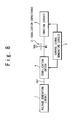
- FIG. 8 schematically shows the configuration of the semiconductor integrated circuit according to the present invention.
- This semiconductor integrated circuit contains a voltage generating circuit 1 , a function circuit 2 , a stabilization capacitance 3 , a stabilization switch 4 and a control signal generating circuit 5 .
- the function circuit 2 operates in accordance with a voltage Vp 1 generated by the voltage generating circuit 1 .
- the voltage Vp 1 generated by the voltage generating circuit 1 is referred to as “Internal Voltage” or “Reference Voltage”.
- One end of the stabilization capacitance 3 is connected to a first node N 1 between the voltage generating circuit 1 and the function circuit 2 .
- the other end of the stabilization capacitance 3 is connected to a terminal of a power supply voltage Vdd or a terminal of a ground GND.
- the stabilization switch 4 is provided between the voltage generating circuit 1 and the first node N 1 .
- the control signal generating circuit 5 generates a control signal for activating/deactivating the function circuit 2 to output to the circuit 2 . Also, the control signal generating circuit 5 generates a switch control signal for turning on/turning off the stabilization switch 4 to output to the switch 4 .
- the function circuit 2 is assumed to be activated at a first time and deactivated at a second time. At this time, according to the present invention, the stabilization switch 4 is turned off simultaneously with the first time or at a predetermined time previous to the first time. Also, the stabilization switch 4 is turned on simultaneously with the second time or at a predetermined time after the second time. That is, the stabilization switch 4 is turned off at least for a period during which the function circuit 2 is activated.
- the present invention will be described below in further detail by exemplifying an MRAM as the semiconductor integrated circuit.
- the magnetic tunnel junction (MTJ) element is used as the memory cell (storing element).
- FIG. 9 is a block diagram showing the configuration of the MRAM according to the first exemplary embodiment of the present invention.
- This MRAM contains a memory cell array 10 , an X-side constant current source circuit 20 , an X-side selector 21 , an X-side current termination circuit 22 , a Y-side constant current source circuit 30 , a Y-side selector 31 , a Y-side current termination circuit 32 and a sense amplifier circuit 33 .
- the MRAM contains the voltage generating circuit 1 , the stabilization capacitances 3 , the stabilization switches (SSW) 4 and the control signal generating circuit 5 that are shown in FIG. 8 .
- the X-side constant current source circuit 20 or the Y-side constant current source circuit 30 corresponds to the function circuit 2 , and this operates in accordance with the voltage generated by the voltage generating circuit 1 .
- the stabilization capacitance 3 is inserted in parallel between the voltage generating circuit 1 and the current source circuits 20 and 30 .
- the stabilization switch 4 is provided between the voltage generating circuit 1 and the stabilization capacitance 3 .
- the control signal generating circuit 5 supplies a decoder activation signal XDENW to the X-side selector (X-side decoder) 21 and the Y-side selector (Y-side decoder) 31 . Also, the control signal generating circuit 5 supplies a write signal WCSEN to the current source circuits 20 and 30 .
- the power supply voltage Vdd corresponds to the High level (H)
- the ground Gnd corresponds to the Low level (L).
- the voltage generating circuit 1 generates an output voltage Vp 1 ( ⁇ the power supply voltage Vdd). Specific configuration examples of the voltage generating circuit 1 are shown in FIG. 10A to FIG. 10D .
- the voltage generating circuit 1 contains a reference voltage generating circuit 51 and a voltage converting circuit 52 .
- the reference voltage generating circuit 51 contains diodes D 0 to D 2 and resistances R 1 and R 2 .
- the voltage converting circuit 52 includes resistances R 3 and R 4 .
- a voltage V 0 is a constant voltage without any temperature dependence that is generated by a different voltage generating circuit.
- V F is a junction potential of the diode D 2
- N is a junction area ratio of the diodes D 0 and D 1
- k B is a Boltzmann constant
- q is a charge amount.
- the output voltage Vp 1 is determined in accordance with the settings of the parameters R 1 to R 4 , N and V 0 .
- the diode is replaced by a PNP bipolar transistor.
- the reference voltage generating circuit 51 of an amplifying type is used.
- the voltage converting circuit 52 of a resistance division type is used.
- FIG. 11 is a circuit diagram showing a part of the configuration shown in FIG. 9 in detail.
- the X-side write circuit will be described.
- the output of the voltage generating circuit 1 is connected to the input of the X-side constant current source circuit 20 (hereinafter, to be referred to as a write current source) through parasitic resistances r 1 and r 2 by the wirings, and the stabilization switch 4 .
- the output voltage Vp 1 ( ⁇ the power supply voltage Vdd) generated by the voltage generating circuit 1 is supplied to the write current source 20 .
- An input voltage supplied to the write current source 20 is assumed to be Vp 2 .
- the stabilization capacitance 3 is connected to the node N 1 between the voltage generating circuit 1 and the write current source 20 . Its capacitance value Cp is different, depending on an application field, and are such as several 10 pF to several 10 nF.
- the stability of the voltage Vp 2 is improved by this stabilization capacitance 103 , and the voltage Vp 2 is kept constant.
- the write current source 20 has a Pch transistor (current source) MP and a switch MPS.
- the voltage Vp 2 is applied to the gate of the Pch transistor MP.
- the input voltage Vp 2 to the write current source 20 is the gate voltage of the Pch transistor MP.
- ⁇ p is the mobility
- W is a gate width
- L is a gate length
- V tp is the threshold voltage.
- the switch MPS is provided between the node NB and the output node NA of the write current source 20 . It should be noted that the parasitic capacitance Cc is accompanied in the Pch transistor MP.
- the output node NA in the write current source 20 is connected through the X-side selector (X-side decoder) 21 to the memory cell array 10 .
- the X-side selector 21 activates one selection line in accordance with a logical product of the decoder activation signal XDENW and the address signal XAn. Also, when the write signal WCSEN becomes High, the switch MPS is turned on. Consequently, the write current Iw from the write current source 20 is supplied to the memory cell (data storing element) 11 or the vicinity thereof.
- the write signal WCSEN is a signal for activating the write current source 20 .
- the write current source 20 generates a predetermined write current Iw based on the voltage Vp 2 from the voltage generating circuit 1 in response to the write signal WCSEN.
- the X-side selector (X-side decoder) 21 is activated in response to the decoder activation signal XDENW to supply the predetermined write current Iw to the memory cell array 10 .
- the stabilization switch (SSW) 4 is interposed between the voltage generating circuit 1 and the first node N 1 .
- the stabilization switch 4 includes a transfer gate composed of a Pch transistor 41 and an Nch transistor 42 , and an inverter 43 .
- the decoder activation signal XDENW is supplied to this stabilization switch 4 from the control signal generating circuit 5 .
- the decoder activation signal XDENW is supplied to the gate of the Pch transistor 41 and also supplied through the inverter 43 to the gate of the Nch transistor 42 .
- the stabilization switch 4 is turned off.
- the stabilization switch 4 operates in synchronization with the decoder activation signal XDENW and is turned on or turned off in response to the decoder activation signal XDENW.
- FIG. 12 is a diagram of timing charts showing the operation of the semiconductor integrated circuit having such a configuration.
- the decoder activation signal XDENW, the write signal WCSEN, the voltage VA of the output node NA, the voltage VB of the node NB, the gate voltage Vp 2 of the Pch transistor MP (the current source) and the current Ip flowing through the parasitic resistance r 1 are shown.
- the respective signals are assumed such that the power supply voltage Vdd corresponds to the High level (H), and the ground Gnd corresponds to the Low level (L).
- the operation of the semiconductor integrated circuit according to this exemplary embodiment will be described below with reference to FIG. 11 and FIG. 12 .
- the stabilization switch 4 is turned on.
- the gate voltage Vp 2 of the Pch transistor MP is equal to the output voltage Vp 1 ( ⁇ the power supply voltage Vdd) of the voltage generating circuit 1 .
- the voltage VA of the output node NA is Low
- the voltage VB of the node NB is High.
- the stabilization switch 4 is turned off, and the first node N 1 is electrically disconnected from the voltage generating circuit 1 .
- the circuit composed of the current source MP, the stabilization capacitance 3 , the stabilization switch 4 and the parasitic capacitance Cc is opened, thereby holding an internal charge amount.
- the current Ip slightly flows through the parasitic resistance r 1 , this is a noise due to the parasitic capacitance of the stabilization switch 4 .
- the current Ip is a current having no relation with the voltage Vp 2 , and has no influence on the write current source 20 .
- the write signal WCSEN becomes High.
- the write current source 20 is activated, and the switch MPS is turned on. Consequently, the voltage VB of the node NB sharply falls toward the Low level.
- the gate voltage Vp 2 is decreased because of the coupling of the parasitic capacitance Cc in the current source MP.
- the gate voltage Vp 2 becomes lower than the voltage level Vp 1 .
- the stabilization switch 4 since the stabilization switch 4 is turned off, there is no current path from the voltage generating circuit 1 to the stabilization capacitance 3 . Therefore, the current does not flow into the stabilization capacitance 3 . In this way, it is important that the stabilization switch 4 is turned off previously to the time ti by a predetermined time. The stabilization switch 4 is turned off at least simultaneously with the time t 1 .
- the write signal WCSEN becomes Low.
- the write current source 20 is deactivated, and the switch MPS is turned off.
- the voltage of the node NB sharply returns to Vdd.
- the gate voltage Vp 2 is increased because of the coupling of the parasitic capacitance Cc.
- the stabilization switch 4 since the stabilization switch 4 is turned off, the current does not flow into or from the circuit composed of the current source MP, the stabilization capacitance 3 , the stabilization switch 4 and the parasitic capacitance Cc. Therefore, the gate voltage Vp 2 is stabilized to the level prior to the activation of the write signal WCSEN, namely, the voltage level Vp 1 .
- the stabilization switch 4 is turned on, and the first node N 1 and the voltage generating circuit 1 are electrically connected. As a result, the gate voltage Vp 2 is held at the level of the output voltage Vp 1 of the voltage generating circuit 1 . In this way, at the time of the completion of a first write operation, a difference is never generated between the gate voltage Vp 2 and the voltage level Vp 1 . Thus, the accumulative voltage variation can be prevented. It is important that the stabilization switch 4 is turned on by a predetermined time after the time t 3 . At least simultaneously with the time t 3 , the stabilization switch 4 is turned on.
- the write operation is performed similarly to the write operation in the period between the time t 1 and the time t 3 .
- the difference is not generated between the gate voltage Vp 2 and the voltage level Vp 1 . Also, the difference is never generated even in the write operation at this time. In this way, the accumulative variation of the voltage Vp 2 can be prevented.
- the control signal generating circuit 5 outputs the write signal WCSEN of the High level to the write current source 20 , after the output of the decoder activation signal XDENW of the High level. Also, the control signal generating circuit 5 outputs the write signal XDENW of the Low level to the write current source 20 , prior to the output of the decoder activation signal XDENW of the Low level. Consequently, the stabilization switch 4 is turned off at least for the period during which the write current source 20 is activated.
- FIG. 13 shows the result of the SPICE simulation with regard to the foregoing circuit and the result corresponds to that of FIG. 7 .
- FIG. 13 shows the variation in the voltage Vp 2 when the write operation is carried out 1000 times at the speed of 100 MHz.
- the voltage level Vp 1 is assumed to be 675 mV.
- the voltage Vp 2 is varied by about 7 mV for each write operation.
- this variation is not a problem because this is equal every time.
- the long-term variation amount ⁇ Vc of the voltage Vp 2 is known to be about 0.2 mV.
- the voltage variation of this degree can be substantially ignored with regard to the operation of the current source.
- the stable write current Iw can be supplied for the long term.
- the internal voltage from the voltage generating circuit 1 is instantly stabilized, and the voltage variation is not accumulated.
- the long-term voltage variation is prevented, thereby insuring that the internal voltage from the voltage generating circuit 1 is stabilized for the long term.
- the reliability of the semiconductor integrated circuit is improved.
- the internal voltage is used to generate the write current Iw. Therefore, the stable write current Iw can be supplied to the memory cell array for the long term. This fact is preferable for the MRAM in which the high precision is required for the write current Iw.
- the internal voltage from the voltage generating circuit 1 is instantly stabilized.
- the function circuit 2 can immediately perform the next operation. That is, the operation speed of the semiconductor integrated circuit is improved. In this way, according to this exemplary embodiment, the semiconductor integrated circuit and the MRAM that have the excellent reliability, yield and operation speed are provided.
- the semiconductor integrated circuit according to the second exemplary embodiment will be described below.
- the voltage variation in the output voltage Vp 1 that is caused by the coupling noise current Ip (refer to FIG. 12 ) in the first exemplary embodiment is reduced.
- this exemplary embodiment is especially preferable.
- FIG. 14 is a block diagram showing the configuration of the MRAM according to the second exemplary embodiment and corresponds to FIG. 9 in the first exemplary embodiment.
- the same reference numerals and symbols are assigned to the same components as those of FIG. 9 , and the explanations are properly omitted.
- the stabilization capacitances 3 are inserted in parallel between the current source circuits (the function circuits) 20 and 30 and the stabilization switches 4 .
- the stabilization switch 4 is provided between the voltage generating circuit 1 and each of the stabilization capacitances 3 .
- a stabilization capacitance 6 is inserted in parallel between the voltage generating circuit 1 and each of the stabilization switches 4 .
- FIG. 15 is a circuit diagram showing a part of the configuration shown in FIG. 14 in detail, and corresponds to FIG. 11 in the first exemplary embodiment.
- the stabilization capacitance 3 (its capacitance value Cp 1 ) is connected to the first node N 1 between the write current source 20 and the stabilization switch (SSW) 4 .
- the stabilization switch 4 is provided between the voltage generating circuit 1 and the first node N 1 .
- one end of another stabilization capacitance 6 (its capacitance value Cp 2 ) is connected to the second node N 2 between the voltage generating circuit 1 and the stabilization switch 4 .
- the other end of the stabilization capacitance 6 is connected to the terminal of the power supply voltage Vdd.
- another function circuit 2 ′ is connected to the second node N 2 .
- the function circuit 2 ′ operates by using the output voltage Vp 1 of the voltage generating circuit 1 .
- FIG. 16 is a diagram showing timing charts of the operation of the semiconductor integrated circuit having such a configuration.
- the decoder activation signal XDENW, the write signal WCSEN, the voltage VA of the output node NA, the voltage VB of the node NB, the gate voltage Vp 2 of the Pch transistor MP (current source) and the current Ip flowing through the parasitic resistance r 1 are shown.
- the respective signals are assumed in such a manner that the power supply voltage Vdd corresponds to the High level (H), and the ground Gnd corresponds to the Low level (L).
- the operation according to this exemplary embodiment will be described below with reference to FIG. 15 and FIG. 16 , as mentioned above.
- the stabilization switch 4 is turned on.
- the gate voltage Vp 2 of the Pch transistor MP is equal to the output voltage Vp 1 ( ⁇ the power supply voltage Vdd) of the voltage generating circuit 1 .
- the voltage VA of the output node NA is Low
- the voltage VB of the node NB is High.
- the stabilization switch 4 is turned off, and the first node N 1 is electrically disconnected from the voltage generating circuit 1 .
- the circuit composed of the current source MP, the stabilization capacitance 3 , the stabilization switch 4 and the parasitic capacitance Cc is opened, thereby holding an internal charge amount.
- the charge is slightly accumulated in a parasitic capacitance of the stabilization switch 4 , and the coupling noise is generated in the first exemplary embodiment.
- the stabilization capacitance 6 is additionally provided, which can substantially remove such coupling noise.
- the output voltage Vp 1 of the voltage generating circuit 1 is used in another function circuit 2 ′, the influence of the coupling does not substantially appear. Thus, this is especially preferable.
- the write signal WCSEN becomes High.
- the write current source 20 is activated, and the switch MPS is turned on. Consequently, the voltage VB of the node NB sharply decreases toward the Low level.
- the gate voltage Vp 2 decreases due to the coupling of the parasitic capacitance Cc in the current source MP.
- the gate voltage Vp 2 becomes lower than the voltage level Vp 1 .
- the stabilization switch 4 is turned off, there is no current path from the voltage generating circuit 1 to the stabilization capacitance 3 . Therefore, the current does not flow into the stabilization capacitance 3 .
- the write signal WCSEN becomes Low.
- the write current source 20 is deactivated, and the switch MPS is turned off.
- the voltage of the node NB sharply returns to Vdd.
- the gate voltage Vp 2 is increased due to the coupling of the parasitic capacitance Cc.
- the stabilization switch 4 since the stabilization switch 4 is turned off, the current does not flow into or from the circuit composed of the current source MP, the stabilization capacitance 3 , the stabilization switch 4 and the parasitic capacitance Cc. Therefore, the gate voltage Vp 2 is stabilized to the level prior to the activation of the write signal WCSEN, namely, the voltage level Vp 1 .
- the stabilization switch 4 is turned on, and the first node N 1 and the voltage generating circuit 1 are electrically connected.
- the gate voltage Vp 2 is held at the level of the output voltage Vp 1 of the voltage generating circuit 1 .
- the difference is never generated between the gate voltage Vp 2 and the voltage level Vp 1 .
- the write operation is performed similarly to the write operation during the period between the time t 1 and the time t 3 .
- the effect similar to the first exemplary embodiment is obtained. That is, the long-term voltage variation is prevented, thereby insuring that the internal voltage from the voltage generating circuit 1 is stabilized for the long term. Thus, the reliability of the semiconductor integrated circuit is improved. Also, the operation speed of the semiconductor integrated circuit is improved. Moreover, according to this exemplary embodiment, it is possible to prevent the voltage variation in the output voltage Vp 1 that is caused by the coupling noise. When the output voltage Vp 1 of the voltage generating circuit 1 is used in another function circuit 2 ′, this exemplary embodiment is especially effective.
- the stabilization switch 4 is applied to an analog circuit that requires a plurality of stabilization capacitances 3 .
- FIG. 17 is a block diagram showing the configuration of the MRAM according to the third exemplary embodiment and corresponds to FIG. 9 in the first exemplary embodiment.
- the same reference numerals and symbols are assigned to the same components as those of FIG. 9 , and the explanations thereof are properly omitted.
- each of the current source circuits (function circuits) 20 and 30 is connected through a plurality of routes to the voltage generating circuit 1 .
- the voltage generating circuit 1 generates a plurality of kinds of voltages (Vp 1 , Vp 3 ) as the reference voltages for the plurality of routes.
- Each of the current source circuits 20 and 30 receives a plurality of kinds of voltages (Vp 2 .
- Vp 4 Vp 4
- the stabilization capacitances 3 ( 3 a , 3 b ) and the stabilization switches 4 ( 4 a , 4 b ) are provided for the plurality of routes.
- FIG. 18 is a circuit diagram showing a part of the configuration shown in FIG. 17 in detail, and corresponds to FIG. 11 in the first exemplary embodiment.
- the same reference numerals and symbols are assigned to the same components as those of FIG. 11 , and the explanations therefore are properly omitted.
- the voltage generating circuit 1 includes a voltage generating circuit 1 a for outputting the output voltage Vp 1 and a voltage generating circuit 1 b for outputting the output voltage Vp 3 .
- the output of the voltage generating circuit 1 a is connected through parasitic resistances r 1 and r 2 and the stabilization switch 4 a to the write current source 20 .
- the stabilization capacitance 3 a (its capacitance value Cpa) is connected to the first node N 1 a between the stabilization switch 4 a and the write current source 20 . Through this group, the voltage Vp 2 is supplied to the write current source 20 .
- the output of the voltage generating circuit 1 b is connected through parasitic resistances r 3 and r 4 and the stabilization switch 4 b to the write current source 20 .
- the stabilization capacitance 3 b (its capacitance value Cpb) is connected to the first node N 1 b between the stabilization switch 4 b and the write current source 20 .
- the voltage Vp 4 is supplied to the write current source 20 .
- the write current source 20 includes Pch transistors (current sources) Mpa and MPb that are cascade-connected.
- the Pch transistor MPa is connected to a node NBa
- the Pch transistor MPb is connected between the node NBa and the node NBb.
- the switch MPS is connected between the node NBb and the output node NA.
- the input voltages Vp 2 and Vp 4 of two groups are required for the sake of the two Pch transistors Mpa and MPb. Specifically, the input voltage Vp 2 is applied as the gate voltage Vp 2 to the gate of the Pch transistor MPa. On the other hand, the input voltage Vp 4 is applied as the gate voltage Vp 4 to the gate of the Pch transistor MPb.
- the parasitic capacitances of the Pch transistors Mpa and MPb are Cca and Ccb, respectively.
- FIG. 19 is a diagram showing timing charts of the operation of the semiconductor integrated circuit having such a configuration.
- the decoder activation signal XDENW, the write signal WCSEN, the voltage VA of the output node NA, the voltage VB of the node NBa or node NBb, the gate voltage Vp 2 of the Pch transistor MPa (current source) and the gate voltage Vp 4 of the Pch transistor MPb (current source) are shown.
- the respective signals are assumed such that the power supply voltage Vdd corresponds to the High level (H), and the ground Gnd corresponds to the Low level (L).
- the operation according to this exemplary embodiment will be described below with reference to FIG. 18 and FIG. 19 , as mentioned above.
- the stabilization switch 4 a ( 4 b ) is turned on.
- the gate voltage Vp 2 (Vp 4 ) is equal to the output voltage Vp 1 (Vp 3 ) of the voltage generating circuit 1 a ( 1 b ).
- the voltage VA of the output node NA is Low
- the voltage VB of the node NBa (NBb) is High.
- the stabilization switch 4 a ( 4 b ) is turned off, and the first node N 1 a (N 1 b ) is electrically disconnected from the voltage generating circuit 1 a ( 1 b ).
- the circuit composed of the current source MPa (MPb), the stabilization capacitance 3 a ( 3 b ), the stabilization switch 4 a ( 4 b ) and the parasitic capacitance Cca (Ccb) is opened, thereby holding an internal charge amount.
- the write signal WCSEN becomes High.
- the write current source 20 is activated, and the switch MPS is turned on. Consequently, the voltage VB of the node NBa (NBb) sharply decreases toward the Low level.
- the gate voltage Vp 2 (Vp 4 ) decreases due to the coupling of parasitic capacitance Cca (Ccb) in the current source MPa (MPb). Thus, at this time point, the gate voltage Vp 2 (Vp 4 ) becomes lower than the voltage level Vp 1 (Vp 3 ).
- the stabilization switch 4 a ( 4 b ) since the stabilization switch 4 a ( 4 b ) is turned off, there is no current path from the voltage generating circuit 1 a ( 1 b ) to the stabilization capacitance 3 a ( 3 b ). Therefore, the current does not flow into the stabilization capacitance 3 a ( 3 b ).
- the write signal WCSEN becomes Low.
- the write current source 20 is deactivated, and the switch MPS is turned off.
- the voltage of the node NBa (NBb) sharply returns to Vdd.
- the gate voltage Vp 2 (Vp 4 ) increases by the coupling of the parasitic capacitance Cca (Ccb).
- the stabilization switch 4 a ( 4 b ) is turned off, the current does not flow into or from the circuit composed of the current source MPa (MPb), the stabilization capacitance 3 a ( 3 b ), the stabilization switch 4 a ( 4 b ) and the parasitic capacitance Cca (Ccb). Therefore, the gate voltage Vp 2 (Vp 4 ) is stabilized to the level prior to the activation of the write signal WCSEN, namely, the voltage level Vp 1 (Vp 3 ).
- the stabilization switch 4 a ( 4 b ) is turned on, and the first node N 1 a (N 1 b ) and the voltage generating circuit 1 a ( 1 b ) are electrically connected.
- the gate voltage Vp 2 (Vp 4 ) is held at the level of the output voltage Vp 1 (Vp 3 ) of the voltage generating circuit 1 a ( 1 b ).
- the difference is never generated between the gate voltage Vp 2 (Vp 4 ) and the voltage level Vp 1 (Vp 3 ).
- the accumulative voltage variation is prevented.
- the write operation is performed similarly to the write operation during the period between the time t 1 and the time t 3 .
- the effect similar to the first exemplary embodiment is obtained. That is, the long-term voltage variation is prevented, thereby insuring that the internal voltage from the voltage generating circuit 1 is stabilized for the long term. Thus, the reliability of the semiconductor integrated circuit is improved. Also, the operation speed of the semiconductor integrated circuit is improved. It should be noted that the second exemplary embodiment and the third exemplary embodiment can be combined.
- the stabilization switch 4 operates in synchronization with the decoder activation signal XDENW. In the fourth exemplary embodiment, the stabilization switch 4 operates at the timing that is not based on the decoder activation signal XDENW. Thus, even when the continuous write operation is performed, the gate voltage Vp 2 can be stabilized.
- FIG. 20 shows the decoder activation signal XDENW, the write signal WCSEN, and the gate voltage Vp 2 .
- the decoder activation signal XDENW is changed to High.
- the write operation is continuously performed. Specifically, the continuous write operation is performed by continuously activating the write signal WCSEN at each of the times t 1 , t 2 , - - - , t 8 , or continuously changing write target addresses (not shown).
- the level of the decoder activation signal XDENW is kept High.
- the terminal to which the gate voltage Vp 2 is supplied is electrically disconnected from the voltage generating circuit 1 , and this is in a high impedance (Hi-Z) state.
- the circuit composed of the current source MP, the stabilization capacitance 3 , the stabilization switch 4 and the parasitic capacitance Cc is opened.
- the internal charge amount is held in principle. Therefore, after each write operation, the gate voltage Vp 2 ought to be held at the voltage level Vp 1 .
- the gate voltage Vp 2 is varied, as shown in FIG. 20 .
- the variation in the gate voltage Vp 2 that is caused by this leakage current is represented by ⁇ Vp 2 .
- the decoder activation signal XDENW becomes Low at a time t 9 , the voltage generating circuit 1 and the current source 20 are finally connected.
- the gate voltage Vp 2 is returned to the voltage level Vp 1 .
- the time while the voltage generating circuit 1 and the write current source 20 are connected is desired to be reserved as much as possible. To do so, ON/OFF of the stabilization switch 4 is required to be controlled in response to a signal other than the decoder activation signal XDENW.
- FIG. 21 is a block diagram showing the configuration of the MRAM according to the fourth exemplary embodiment and corresponds to FIG. 9 in the first exemplary embodiment.
- the control signal generating circuit 5 outputs the write signal WCSEN to a signal converting circuit 7 .
- the signal converting circuit 7 generates a first control signal OUT 1 and a second control signal OUT 2 in response to the input write signal WCSEN.
- the first control signal OUT 1 functions as the decoder activation signal XDENW in the above-mentioned exemplary embodiments, and this is supplied to the X-side selector 21 , the Y-side selector 31 and the stabilization switch 4 .
- the second control signal OUT 2 functions as the write signal WCSEN in the above-mentioned exemplary embodiments, and this is supplied to the X-side constant current source circuit 20 and the Y-side constant current source circuit 30 .
- FIG. 22 is a circuit diagram showing a part of the configuration shown in FIG. 21 in detail and corresponds to FIG. 11 in the first exemplary embodiment.
- the same reference numerals and symbols are assigned to the same components as those FIG. 11 , and the explanations thereof are properly omitted.
- the X-side selector 21 activates one selection line in accordance with a logical product of the first control signal OUT 1 and an address signal XAn.
- the first control signal OUT 1 is a control signal for activating the X-side selector (X-side decoder) 21 .
- the switch MPS of the write current source 20 is turned on. Consequently, the write current Iw from the write current source 20 is supplied to the memory cell (data storing element) 11 or the vicinity thereof.
- the second control signal OUT 2 is a signal for activating the write current source 20 .
- the stabilization capacitance 3 is connected to the first node N 1 between the write current source 20 and the stabilization switch (SSW) 4 .
- the stabilization switch 4 is provided between the voltage generating circuit 1 and the first node N 1 .
- FIG. 22 shows one example of the configuration of the signal converting circuit 7 .
- the signal converting circuit 7 is provided with delay elements 71 and 72 , multiplexers 73 and 74 and an inverter 75 .
- the write signal WCSEN is supplied as a signal WCSEN 1 to the delay element 71 and data terminals D 0 of the multiplexers 73 and 74 .
- a signal WCSEN 2 outputted by the delay element 71 is supplied to the delay element 72 and data terminals D 1 of the multiplexers 73 and 74 .
- a signal WCSEN 3 outputted by the delay element 72 is supplied to an input terminal A of the multiplexer 73 and an input terminal A of the multiplexer 74 through the inverter 75 .
- Each of the multiplexers 73 and 74 is designed to output the signal on the data terminal D when the input A is at the Low level, and output the signal on the data terminal D 1 when the input A is'at the High level.
- the output signal of the multiplexer 73 is the first control signal OUT 1
- the output signal of the multiplexer 74 is the second control signal OUT 2 .
- FIG. 23 A diagram showing the operation timing charts of the thus-configured signal converting circuit 7 is shown in FIG. 23 .
- the write signal WCSEN (WCSEN 1 ) becomes High at a time t 0
- the signal WCSEN 2 becomes High at a time t 1 after a time tD.
- the signal WCSEN 3 becomes High at a time t 2 after the time tD.
- the write signal WCSEN (WCSEN 1 ) becomes Low at a time t 3
- the signal WCSEN 2 becomes Low at a time t 4 after the time tD.
- the signal WCSEN 3 becomes Low at a time t 5 after the time tD.
- the signal WCSEN 2 is a signal after delayed by a delay time tD from the signal WCSEN 1
- the signal WCSEN 3 is a signal after delayed by a delay time 2tD from the signal WCSEN 1 .
- Such signals WCSEN 1 to WCSEN 3 determine the first control signal OUT 1 and the second control signal OUT 2 .
- the first control signal OUT 1 rises at the time t 0 and falls at the time t 4 .
- the second control signal OUT 2 rises at the time t 1 and falls at the time t 3 .
- the first control signal OUT 1 is generated, which rises earlier than the second control signal OUT 2 and falls later than the second control signal OUT 2 .
- the stabilization switch 4 can be turned off for the period during while the write current source 20 is activated at least.
- the timings of the first control signal OUT 1 and the second control signal OUT 2 can be freely set by the delay elements 71 and 72 .
- FIG. 24 is a diagram showing timing charts of the operation of the semiconductor integrated circuit having the foregoing configuration.
- FIG. 24 shows the write signal WCSEN, the first control signal OUT 1 , the second control signal OUT 2 and the gate voltage Vp 2 of the Pch transistor MP (current source).
- the continuous write operation according to this exemplary embodiment will be described below with reference to FIG. 22 and FIG. 24 as mentioned above.
- the first control signal OUT 1 is also Low, and the stabilization switch 4 is turned on.
- the gate voltage Vp 2 of the Pch transistor MP is equal to the output voltage Vp 1 ( ⁇ the power supply voltage Vdd) of the voltage generating circuit 1 .
- the voltage VA of the output node NA is Low, and the voltage VB of the node NB is High.
- the write signal WCSEN is changed to High. Consequently, the first control signal OUT 1 is also changed to High. As a result, the stabilization switch 4 is turned off, and the first node N 1 is electrically disconnected from the voltage generating circuit 1 . Thus, the circuit composed of the current source MP, the stabilization capacitance 3 , the stabilization switch 4 and the parasitic capacitance Cc is opened, thereby holding an internal charge amount.
- the second control signal OUT 2 becomes High.
- the write current source 20 is activated, and the switch MPS is turned on.
- the voltage VB of the node NB sharply decreases toward the Low level.
- the gate voltage Vp 2 decreases due to the coupling of the parasitic capacitance Cc of the current source MP.
- the gate voltage Vp 2 is lower than the voltage level Vp 1 .
- the stabilization switch 4 is turned off, there is no current route from the voltage generating circuit 1 and the stabilization capacitance 3 . Therefore, the current does not flow into the stabilization capacitance 3 .
- the write signal WCSEN is changed to Low. Consequently, the second control signal OUT 2 is also changed to Low.
- the write current source 20 is deactivated, and the switch MPS is turned off.
- the voltage of the node NB sharply returns to Vdd%
- the gate voltage Vp 2 increases due to the coupling of the parasitic capacitance Cc.
- the stabilization switch 4 is turned off, the current does not flow into or from the circuit composed of the current source MP, the stabilization capacitance 3 , the stabilization switch 4 and the parasitic capacitance Cc.
- the gate voltage Vp 2 is stabilized to the level prior to the activation of the write signal WCSEN, namely, the voltage level Vp 1 .
- the gate voltage Vp 2 becomes at the level slightly different from the voltage level Vp 1 .
- the write activation time is very short, such as several ns to several 10 ns, and the variation amount is equal every time.
- the first control signal OUT 1 becomes Low.
- the stabilization switch 4 is turned on, and the first node N 1 and the voltage generating circuit 1 are electrically connected.
- the gate voltage Vp 2 is held at the level of the output voltage Vp 1 of the voltage generating circuit 1 .
- This state is held in the period until the next write operation (until t 4 ).
- the accumulative voltage variation is prevented, thereby supplying the stable write current Iw for the long term.
- the effect similar to the first exemplary embodiment is obtained. That is, the long-term voltage variation is prevented, thereby insuring that the internal voltage from the voltage generating circuit 1 is stabilized for the long term. Thus, the reliability of the semiconductor integrated circuit is improved. Also, the operation speed of the semiconductor integrated circuit is improved. Moreover, according to this exemplary embodiment, it is possible to suppress the variation in the gate voltage Vp 2 during the continuous write process period. It should be noted that this exemplary embodiment can be applied to the second exemplary embodiment and the third exemplary embodiment.
- the stabilization switch 4 is added between the stabilization capacitance 3 and the voltage generating circuit 1 , the long-term variation in the voltage can be removed in principle.
- the semiconductor integrated circuit is provided that can be stably operated at the high speed.
Landscapes
- Engineering & Computer Science (AREA)
- Computer Hardware Design (AREA)
- Power Engineering (AREA)
- Semiconductor Memories (AREA)
- Mram Or Spin Memory Techniques (AREA)
- Semiconductor Integrated Circuits (AREA)
- Logic Circuits (AREA)
- Static Random-Access Memory (AREA)
Abstract
Description
ΔVc=[Q(+)−Q(−)]/Cp
corresponds to the voltage variation in the voltage Vp2.
Vp1=(1+R4/R3)V 0−(R4/R3)(V F +k B T/q(R2/R1)ln(N)).
Here, VF is a junction potential of the diode D2, and N is a junction area ratio of the diodes D0 and D1, kB is a Boltzmann constant, and q is a charge amount. The output voltage Vp1 is determined in accordance with the settings of the parameters R1 to R4, N and V0.
Vp1=1/(1+R4/R3)(V F +k B T/q(R2/R1)ln(N)).
Claims (20)
Applications Claiming Priority (4)
| Application Number | Priority Date | Filing Date | Title |
|---|---|---|---|
| JP2005332391 | 2005-11-17 | ||
| JP2005332391 | 2005-11-17 | ||
| JP2005-332391 | 2005-11-17 | ||
| PCT/JP2006/322185 WO2007058088A1 (en) | 2005-11-17 | 2006-11-07 | Semiconductor integrated circuit |
Publications (2)
| Publication Number | Publication Date |
|---|---|
| US20100067292A1 US20100067292A1 (en) | 2010-03-18 |
| US7764552B2 true US7764552B2 (en) | 2010-07-27 |
Family
ID=38048476
Family Applications (1)
| Application Number | Title | Priority Date | Filing Date |
|---|---|---|---|
| US12/085,158 Active 2027-07-17 US7764552B2 (en) | 2005-11-17 | 2006-11-07 | Semiconductor integrated circuit |
Country Status (3)
| Country | Link |
|---|---|
| US (1) | US7764552B2 (en) |
| JP (1) | JP4957913B2 (en) |
| WO (1) | WO2007058088A1 (en) |
Families Citing this family (1)
| Publication number | Priority date | Publication date | Assignee | Title |
|---|---|---|---|---|
| US8107280B2 (en) * | 2008-11-05 | 2012-01-31 | Qualcomm Incorporated | Word line voltage control in STT-MRAM |
Citations (8)
| Publication number | Priority date | Publication date | Assignee | Title |
|---|---|---|---|---|
| US4276615A (en) * | 1979-09-28 | 1981-06-30 | Graphic Arts Manufacturing Company | Analog read-only memory system for antilog conversion |
| JP2002111470A (en) | 2000-10-03 | 2002-04-12 | Hitachi Ltd | Semiconductor device |
| JP2002208275A (en) | 2001-01-11 | 2002-07-26 | Matsushita Electric Ind Co Ltd | Semiconductor integrated circuit and inspection method thereof |
| US20030007296A1 (en) | 2001-07-06 | 2003-01-09 | Mitsubishi Denki Kabushiki Kaisha | Semiconductor integrated circuit device with internal power supply potential generation circuit |
| JP2004220759A (en) | 2002-12-27 | 2004-08-05 | Toshiba Corp | Semiconductor storage device |
| JP2004234816A (en) | 2003-01-06 | 2004-08-19 | Nec Corp | Semiconductor memory |
| US20040165472A1 (en) | 2003-02-24 | 2004-08-26 | Renesas Technology Corp. | Pseudo-static synchronous semiconductor memory device |
| US20040232974A1 (en) | 2003-05-19 | 2004-11-25 | Mitsubishi Denki Kabushiki Kaisha | Voltage generating circuit |
Family Cites Families (1)
| Publication number | Priority date | Publication date | Assignee | Title |
|---|---|---|---|---|
| US5959471A (en) * | 1997-09-25 | 1999-09-28 | Siemens Aktiengesellschaft | Method and apparatus for reducing the bias current in a reference voltage circuit |
-
2006
- 2006-11-07 US US12/085,158 patent/US7764552B2/en active Active
- 2006-11-07 WO PCT/JP2006/322185 patent/WO2007058088A1/en not_active Ceased
- 2006-11-07 JP JP2007545199A patent/JP4957913B2/en not_active Expired - Fee Related
Patent Citations (12)
| Publication number | Priority date | Publication date | Assignee | Title |
|---|---|---|---|---|
| US4276615A (en) * | 1979-09-28 | 1981-06-30 | Graphic Arts Manufacturing Company | Analog read-only memory system for antilog conversion |
| JP2002111470A (en) | 2000-10-03 | 2002-04-12 | Hitachi Ltd | Semiconductor device |
| JP2002208275A (en) | 2001-01-11 | 2002-07-26 | Matsushita Electric Ind Co Ltd | Semiconductor integrated circuit and inspection method thereof |
| US20030007296A1 (en) | 2001-07-06 | 2003-01-09 | Mitsubishi Denki Kabushiki Kaisha | Semiconductor integrated circuit device with internal power supply potential generation circuit |
| JP2003022697A (en) | 2001-07-06 | 2003-01-24 | Mitsubishi Electric Corp | Semiconductor integrated circuit device |
| JP2004220759A (en) | 2002-12-27 | 2004-08-05 | Toshiba Corp | Semiconductor storage device |
| JP2004234816A (en) | 2003-01-06 | 2004-08-19 | Nec Corp | Semiconductor memory |
| US20040165472A1 (en) | 2003-02-24 | 2004-08-26 | Renesas Technology Corp. | Pseudo-static synchronous semiconductor memory device |
| JP2004259318A (en) | 2003-02-24 | 2004-09-16 | Renesas Technology Corp | Synchronous semiconductor memory device |
| US20040232974A1 (en) | 2003-05-19 | 2004-11-25 | Mitsubishi Denki Kabushiki Kaisha | Voltage generating circuit |
| JP2005006489A (en) | 2003-05-19 | 2005-01-06 | Mitsubishi Electric Corp | Voltage generation circuit |
| US20060028266A1 (en) | 2003-05-19 | 2006-02-09 | Mitsubishi Denki Kabushiki Kaisha | Voltage generating circuit |
Non-Patent Citations (1)
| Title |
|---|
| Takeshi Honda, et al., MRAM-Writing Circuitry to Compensate for Thermal-Variation of Magnetization-Reversal Current, 2002 Symposium on VLSI Circuits Digest of Technical Papers, 2002, Fig. 4. |
Also Published As
| Publication number | Publication date |
|---|---|
| US20100067292A1 (en) | 2010-03-18 |
| JP4957913B2 (en) | 2012-06-20 |
| WO2007058088A1 (en) | 2007-05-24 |
| JPWO2007058088A1 (en) | 2009-04-30 |
Similar Documents
| Publication | Publication Date | Title |
|---|---|---|
| US5600281A (en) | Oscillator circuit generating a clock signal having a temperature dependent cycle and a semiconductor memory device including the same | |
| US20020057618A1 (en) | Semiconductor integrated circuit device having hierarchical power source arrangement | |
| US6473343B2 (en) | Signal amplification circuit for amplifying and sensing current difference and semiconductor memory device including same | |
| US7869294B2 (en) | Semiconductor device having single-ended sensing amplifier | |
| JPH09231751A (en) | Semiconductor memory device | |
| KR102435906B1 (en) | Memory device and operating method of memory device | |
| CN107958678B (en) | Sense amplifier circuit | |
| KR940003402B1 (en) | Dynamic Random Access Memory Device | |
| KR960006377B1 (en) | Word Line Loading Compensation Circuit of Semiconductor Memory Device | |
| JP2004054547A (en) | Bus interface circuit and receiver circuit | |
| US6404677B2 (en) | Semiconductor memory device capable of performing stable read operation and read method thereof | |
| US7277342B2 (en) | Semiconductor memory having dummy bit line precharge/discharge circuit | |
| US7764552B2 (en) | Semiconductor integrated circuit | |
| US7808843B2 (en) | Integrated circuit and method of operating the same | |
| US6717875B2 (en) | Semiconductor memory device | |
| US4610003A (en) | Dynamic type semiconductor memory device | |
| US7248518B2 (en) | Self-timed memory device providing adequate charging time for selected heaviest loading row | |
| US20070019464A1 (en) | Magnetic memory device | |
| JPH05205480A (en) | Word-line driver circuit | |
| JP4830437B2 (en) | Magnetic random access memory | |
| KR100301820B1 (en) | Sense amplifier | |
| US7599230B2 (en) | Semiconductor memory apparatus and method of driving the same | |
| US7821815B2 (en) | Memory cell and semiconductor memory device having thereof memory cell | |
| JPH0822693A (en) | Semiconductor memory device | |
| JP2953102B2 (en) | Semiconductor memory device |
Legal Events
| Date | Code | Title | Description |
|---|---|---|---|
| AS | Assignment |
Owner name: NEC CORPORATION,JAPAN Free format text: ASSIGNMENT OF ASSIGNORS INTEREST;ASSIGNORS:HONDA, TAKESHI;SAKIMURA, NOBORU;SUGIBAYASHI, TADAHIKO;REEL/FRAME:020996/0154 Effective date: 20080422 |
|
| STCF | Information on status: patent grant |
Free format text: PATENTED CASE |
|
| FPAY | Fee payment |
Year of fee payment: 4 |
|
| MAFP | Maintenance fee payment |
Free format text: PAYMENT OF MAINTENANCE FEE, 8TH YEAR, LARGE ENTITY (ORIGINAL EVENT CODE: M1552) Year of fee payment: 8 |
|
| MAFP | Maintenance fee payment |
Free format text: PAYMENT OF MAINTENANCE FEE, 12TH YEAR, LARGE ENTITY (ORIGINAL EVENT CODE: M1553); ENTITY STATUS OF PATENT OWNER: LARGE ENTITY Year of fee payment: 12 |