US7760478B2 - Control circuit with short-circuit protection for current sense terminal of power converters - Google Patents
Control circuit with short-circuit protection for current sense terminal of power converters Download PDFInfo
- Publication number
- US7760478B2 US7760478B2 US11/687,056 US68705607A US7760478B2 US 7760478 B2 US7760478 B2 US 7760478B2 US 68705607 A US68705607 A US 68705607A US 7760478 B2 US7760478 B2 US 7760478B2
- Authority
- US
- United States
- Prior art keywords
- signal
- circuit
- power switch
- protection
- sense
- Prior art date
- Legal status (The legal status is an assumption and is not a legal conclusion. Google has not performed a legal analysis and makes no representation as to the accuracy of the status listed.)
- Active, expires
Links
- 238000001514 detection method Methods 0.000 claims abstract description 9
- 238000012795 verification Methods 0.000 claims abstract description 8
- 239000003990 capacitor Substances 0.000 description 6
- 230000010355 oscillation Effects 0.000 description 5
- 230000001105 regulatory effect Effects 0.000 description 3
- 230000002596 correlated effect Effects 0.000 description 2
- 230000003287 optical effect Effects 0.000 description 2
- 230000002159 abnormal effect Effects 0.000 description 1
- 230000001276 controlling effect Effects 0.000 description 1
- 238000012986 modification Methods 0.000 description 1
- 230000004048 modification Effects 0.000 description 1
- 230000001960 triggered effect Effects 0.000 description 1
Images


Classifications
-
- H—ELECTRICITY
- H02—GENERATION; CONVERSION OR DISTRIBUTION OF ELECTRIC POWER
- H02M—APPARATUS FOR CONVERSION BETWEEN AC AND AC, BETWEEN AC AND DC, OR BETWEEN DC AND DC, AND FOR USE WITH MAINS OR SIMILAR POWER SUPPLY SYSTEMS; CONVERSION OF DC OR AC INPUT POWER INTO SURGE OUTPUT POWER; CONTROL OR REGULATION THEREOF
- H02M1/00—Details of apparatus for conversion
- H02M1/32—Means for protecting converters other than automatic disconnection
-
- H—ELECTRICITY
- H02—GENERATION; CONVERSION OR DISTRIBUTION OF ELECTRIC POWER
- H02M—APPARATUS FOR CONVERSION BETWEEN AC AND AC, BETWEEN AC AND DC, OR BETWEEN DC AND DC, AND FOR USE WITH MAINS OR SIMILAR POWER SUPPLY SYSTEMS; CONVERSION OF DC OR AC INPUT POWER INTO SURGE OUTPUT POWER; CONTROL OR REGULATION THEREOF
- H02M3/00—Conversion of DC power input into DC power output
- H02M3/22—Conversion of DC power input into DC power output with intermediate conversion into AC
- H02M3/24—Conversion of DC power input into DC power output with intermediate conversion into AC by static converters
- H02M3/28—Conversion of DC power input into DC power output with intermediate conversion into AC by static converters using discharge tubes with control electrode or semiconductor devices with control electrode to produce the intermediate AC
- H02M3/325—Conversion of DC power input into DC power output with intermediate conversion into AC by static converters using discharge tubes with control electrode or semiconductor devices with control electrode to produce the intermediate AC using devices of a triode or a transistor type requiring continuous application of a control signal
- H02M3/335—Conversion of DC power input into DC power output with intermediate conversion into AC by static converters using discharge tubes with control electrode or semiconductor devices with control electrode to produce the intermediate AC using devices of a triode or a transistor type requiring continuous application of a control signal using semiconductor devices only
- H02M3/33507—Conversion of DC power input into DC power output with intermediate conversion into AC by static converters using discharge tubes with control electrode or semiconductor devices with control electrode to produce the intermediate AC using devices of a triode or a transistor type requiring continuous application of a control signal using semiconductor devices only with automatic control of the output voltage or current, e.g. flyback converters
-
- H—ELECTRICITY
- H02—GENERATION; CONVERSION OR DISTRIBUTION OF ELECTRIC POWER
- H02M—APPARATUS FOR CONVERSION BETWEEN AC AND AC, BETWEEN AC AND DC, OR BETWEEN DC AND DC, AND FOR USE WITH MAINS OR SIMILAR POWER SUPPLY SYSTEMS; CONVERSION OF DC OR AC INPUT POWER INTO SURGE OUTPUT POWER; CONTROL OR REGULATION THEREOF
- H02M1/00—Details of apparatus for conversion
- H02M1/0003—Details of control, feedback or regulation circuits
- H02M1/0009—Devices or circuits for detecting current in a converter
Definitions
- the present invention relates to control circuits and more specifically relates to a control circuit with short circuit protection for current sense terminal of power converter.
- FIG. 1 shows a traditional power converter.
- the power converter includes a control circuit 10 , which coupled to the output voltage V O of the power converter to generate a switching signal S W at a switching terminal SW of the control circuit 10 for regulating the output voltage V O .
- the switching signal S W is transmitted to a power switch 11 to switch a transformer 12 and control the energy transferred through the transformer 12 .
- a switching current I P of the power switch 11 is generated accordingly.
- the switching current I P is expressed as,
- V IN is an input voltage applied to the transformer 10 ;
- L P is the primary inductance of the transformer 12 ; and
- T ON is an on-time of the switching signal S W .
- the switching current I P generates an input signal V I by a resistor 13 .
- the input signal V I is transmitted to a current sense terminal VI of the control circuit 10 .
- the output voltage V O is generated from the transformer 12 through a rectifier 14 and a capacitor 15 .
- a reference voltage device 17 and a resistor 16 are connected in serial.
- the resistor 16 is connected to the output voltage V O .
- the reference voltage device 17 is connected to an optical isolator 18 .
- the optical isolator 18 generates a feedback signal V FB which is coupled to the control circuit 10 .
- FIG. 2 shows a conventional control circuit 10 of the power converter.
- a comparator 101 is coupled to receive the input signal V I representing the switching current I P of the power switch 11 (as shown in FIG. 1 ). Another input terminal of the comparator 101 is coupled to receive the feedback signal V FB to compare with the input signal V I for the current mode control.
- a resistor 108 is connected to bias the feedback signal V FB .
- the switching signal S W is turned off when the level of the input signal V I is higher than the level of the feedback signal V FB .
- a comparator 102 is coupled to receive the input signal V I as well and is utilized to limit the maximum current of the power switch 11 . The comparator 102 compares the input signal V I with a current-limit threshold V TH .
- the power switch 11 is turned off cycle-by-cycle in response to the output of the comparator 102 when the current limit set by the current-limit threshold V TH is exceeded.
- the comparator 102 would limit the maximum value of the output power.
- the control circuit 10 generates the switching signal S W to drive power switch 11 in response to the feedback signal V FB for regulating the output voltage V O of the power converter.
- An oscillation circuit 103 (OSC) generates a clock signal PLS to the clock-input terminal CK of a flip-flop 104 through an inverter 105 .
- the supply voltage V CC transmits to the D-input terminal D of the flip-flop 104 .
- the reset-input R of the flip-flop 104 is connected to the output terminal of an AND gate 106 .
- the input terminal of the AND gate 106 is connected to the output terminal the comparator 101 .
- Another input terminal of the AND gate 106 is connected to the output terminal of the comparator 102 .
- the output terminal Q of the flip-flop 104 is connected to a AND gate 107 .
- Another input terminal of the AND gate 107 receives the clock signal PLS through the inverter 105 .
- the AND gate 107 generates the switching signal SW from its output terminal.
- the switching signal S W is therefore enabled by the clock signal PLS periodically and is controlled by the feedback signal V FB .
- the switching signal S W is disabled when the switching current I P is higher than the current-limit threshold V TH .
- An objective of the invention is to provide a control circuit that turns off the power switch for the protection when short-circuited is occurred.
- a control circuit with short-circuit protection includes a detection circuit to detect the short-circuited of a current sense terminal of the power converter.
- the detection circuit includes a comparator, a verification circuit and a timer circuit.
- the comparator is coupled to receive an input signal for generating a sense signal.
- the input signal represents the switching current of a power switch.
- the sense signal is enabled when the input signal is lower than a threshold.
- a time delay circuit is utilized to generate a delay signal in response to the enabling of the power switch.
- the verification circuit generates a protection signal in response to the sense signal and the delay signal.
- the protection signal is enabled when the power switch or/and the sense signal are enabled after the time delay of the delay signal.
- the timer circuit is coupled to receive the protection signal for generating a control signal to latch off the power switch.
- the control signal is generated when the protection signal is existed over a time-out period of the timer circuit.
- the control signal is coupled to turn off the power switch for the protection.
- FIG. 1 shows a conventional power converter
- FIG. 2 shows a conventional control circuit of the power converter.
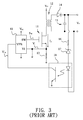
- FIG. 3 shows the short-circuited of a current sense terminal of the control circuit.
- FIG. 4 is a control circuit of the power converter according to present invention.
- FIG. 5 shows an oscillation circuit according to present invention.
- FIG. 6 shows waveforms of the control circuit.
- FIG. 7 is the circuit schematic of the detection circuit according to present invention.
- FIG. 8 is an adder circuit according to present invention.
- FIG. 4 shows a preferred embodiment of a control circuit of the power converter according to present invention.
- the control circuit includes an adder circuit 20 , a detection circuit 21 , an oscillation circuit 22 , two comparators 25 , 26 , two AND gates 27 , 29 , an inverter 23 and a flip-flop 28 .
- the adder circuit 20 is coupled to receive a ramp signal RAMP and an input signal V I for generating a slope signal SLP.
- the input signal V I represents the switching current I P of the power switch 11 (as shown in FIG. 1 ).
- the slope signal SLP is correlated to the sum of the ramp signal RAMP and the input signal V I .
- the oscillation circuit 22 is used to generate the ramp signal RAMP, a time delay signal S N and the clock signal PLS.
- the ramp signal RAMP is in phase with the clock signal PLS.
- the switching signal S W is enabled when the ramp signal RAMP is enabled.
- the comparator 25 is coupled to receive the slope signal SLP.
- Another input terminal of the comparator 25 is coupled to receive the feedback signal V FB to compare with the slope signal SLP for the regulation of the power converter.
- a resistor 24 is connected to bias the feedback signal V FB .
- the switching signal S W is turned off once the level of the slope signal SLP is higher than the level of the feedback signal V FB . Since the slope signal SLP is composed by the ramp signal RAMP and the input signal V I , the feedback operation of the power converter is maintained despite short-circuited of the current sense terminal VI.
- the comparator 26 is coupled to receive the input signal V I as well.
- the comparator 26 is utilized to limit the maximum current of the power switch 11 .
- the comparator 26 compares the input signal V I with a current-limit threshold V TH for limiting the maximum value of the output power.
- the clock signal PLS is transmitted to the clock-input terminal CK of a flip-flop 28 through the inverter 23 .
- a control signal ENB is transmitted to the D-input terminal D of the flip-flop 28 .
- the reset-input terminal R of the flip-flop 28 is connected to the output terminal of an AND gate 27 .
- the input terminal of the AND gate 27 is connected to the output terminal the comparator 25 .
- Another input terminal of the AND gate 27 is connected to the output terminal of the comparator 26 .
- the output terminal Q of the flip-flop 28 is connected to the AND gate 29 to generate the switching signal SW.
- Another input terminal of the AND gate 29 receives the clock signal PLS through the inverter 23 .
- the switching signal S W is thus enabled by the clock signal PLS if the control signal ENB is enabled.
- the switching signal S W controls the power switch 11 .
- the power switch 11 is turned on in response to the falling edge of the pulse signal PLS.
- the switching signal S W is further controlled by the feedback signal V FB and the slope signal SLP.
- the switching signal S W is disabled to protect the power switch 11 , if the switching current I P (the input signal V I ) is higher than the current-limit threshold V TH .
- the detection circuit 21 is coupled to receive the input signal V I , the time delay signal S N , the clock signal PLS and the switching signal S W for generating the control signal ENB.
- FIG. 5 shows the oscillation circuit 250 in the FIG. 4 .
- a current source 221 is coupled to a capacitor 230 through a switch 223 .
- Another current source 222 is coupled to the capacitor 230 through a switch 224 .
- Two comparators 225 and 226 receive trip-point voltages V H and V L respectively.
- the comparator 225 is coupled to the capacitor 230 to generate a first output to the input terminal of an NAND gate 227 .
- the comparator 226 is coupled to the capacitor 230 as well to generate a second output to the input terminal of an NAND gate 228 .
- the NAND gates 227 , 228 connect together to form a RS latch circuit to generate a discharge signal to control the switch 224 .
- the discharge signal also transmits to an inverter 229 and generates a charge signal.
- the charge signal controls the switch 223 , and generates the clock signal PLS through an inverter 231 .
- the ramp signal RAMP is generated at the capacitor 230
- a time delay circuit 23 is used to generate the delay signal S N .
- the time delay circuit 23 receives a reference signal V M and includes a second comparator 232 and an AND gate 233 .
- the trip-point voltage V H is higher than the reference signal V M .
- the reference signal V M is higher than the trip-point voltage V L .
- the second comparator 232 is coupled to receive the ramp signal RAMP for generating a signal S M at the output terminal of the second comparator 232 in response to the ramp signal RAMP and the reference signal V M .
- An Input terminal of an AND gate 233 receives the clock signal PLS through the inverter 231 .
- Another input terminal of the AND gate 233 receives the signal S M for generating the delay signal S N .
- the falling edge of the pulse signal PLS initials the switching signal SW and the delay signal S N .
- the falling edge of the delay signal S N is produced after the time delay TD.
- the pulse width of the delay signal S N represents the time delay TD of the time delay circuit 23 . Waveforms are shown in FIG. 6 .
- FIG. 7 is a preferred circuit schematic of the detection circuit 21 in the FIG. 4 .
- the detection circuit 21 includes a comparator 211 , a verification circuit 213 and a timer circuit 212 .
- the comparator 211 is coupled to receive the input signal V I for generating a sense signal V S .
- the sense signal V S is enabled when the input signal V I is lower than a threshold V R2 .
- the verification circuit 213 includes an AND gate 215 , an inverter 216 and a flip-flip 217 .
- the AND gate 215 is coupled to receive the sense signal V S and the switching signal SW.
- the output terminal of the AND gate 215 is connected to the D-input terminal D of the flip-flop 217 .
- the clock-input terminal CK of the flip-flop 217 receives the delay signal S N through the inverter 216 .
- the verification circuit 213 generates a protection signal V P at the output terminal Q of the flip-flop 217 in response to the sense signal V S and the delay signal S N .
- the protection signal V P is enabled when the power switch 11 or/and the sense signal V S are enabled after the time delay T D of the delay signal S N .
- the timer circuit 212 is coupled to receive the protection signal V P for generating the control signal ENB to latch off the switching signal SW and the power switch 11 .
- the timer circuit 212 includes flip-flips 321 , 322 , . . . , 325 , 326 and an inverter 327 .
- the flip-flop 325 is operated as a counter, which is triggered by the clock signal PLS.
- the reset-input-terminals R of the flip-flops 321 , 322 , . . . , 325 are connected and receive the protection signal V P .
- the output of the counter is used to trigger the flip-flop 326 when the counter is over-flow.
- the flip-flop 326 is operated as a latch to generate the control signal ENB through the inverter 327 .
- the reset-input terminals R of the flip-flop 217 and 326 are connected to a power-on reset signal PWRST.
- the control signal ENB is generated when the protection signal V P is existed over a time-out period of the timer circuit 212 .
- the control signal ENB is used to turn off the power switch 11 for the protection.
- the switching current IP when the power switch 11 is turned on, the switching current IP should be higher than a certain value after the time delay TD. Therefore the current sense terminal VI is predicted as short-circuit if the input signal VI is detected lower than the threshold VR 2 after the time delay TD. Additionally, the timer circuit 212 is used for the debounce of enabling the protection. However, the time-out period of the timer circuit 212 should be limited to ensure the power switch 11 operated under the safe operation area (SOA) during the abnormal condition, such as the output of the power converter and the current sense terminal are short circuited.
- SOA safe operation area
- FIG. 8 is a preferred embodiment of the adder circuit 20 .
- the adder circuit 20 is coupled to receive the ramp signal RAMP to generate the slope signal SLP in accordance with the ramp signal RAMP and the input signal V I .
- An operational amplifier 201 , a transistor 202 and a resistor 203 are operated as a voltage-to-current circuit to generate a current I 1 in response to the ramp signal RAMP.
- Transistors 206 and 207 form a current mirror to generate a current I 2 in accordance with the current I 1 .
- Another operational amplifier 205 is operated as a unit-gain buffer to receive the input signal V I .
- the output terminal of the unit-gain buffer is connected to a resistor 204 .
- the current I 2 is further connected to the resistor 204 , which associates with the unit-gain buffer to generate the slope signal SLP.
- the resistor 204 is correlated with the resistor 203 .
Landscapes
- Engineering & Computer Science (AREA)
- Power Engineering (AREA)
- Inverter Devices (AREA)
- Dc-Dc Converters (AREA)
Abstract
Description
Claims (5)
Priority Applications (3)
| Application Number | Priority Date | Filing Date | Title |
|---|---|---|---|
| US11/687,056 US7760478B2 (en) | 2007-03-16 | 2007-03-16 | Control circuit with short-circuit protection for current sense terminal of power converters |
| TW096121448A TWI335118B (en) | 2007-03-16 | 2007-06-14 | Control circuit with short-circuit protection for current sense terminal of power converters |
| CN2007101279110A CN101267157B (en) | 2007-03-16 | 2007-06-25 | Control circuit for short-circuit protection of current detection end of power converter |
Applications Claiming Priority (1)
| Application Number | Priority Date | Filing Date | Title |
|---|---|---|---|
| US11/687,056 US7760478B2 (en) | 2007-03-16 | 2007-03-16 | Control circuit with short-circuit protection for current sense terminal of power converters |
Publications (2)
| Publication Number | Publication Date |
|---|---|
| US20080232018A1 US20080232018A1 (en) | 2008-09-25 |
| US7760478B2 true US7760478B2 (en) | 2010-07-20 |
Family
ID=39774437
Family Applications (1)
| Application Number | Title | Priority Date | Filing Date |
|---|---|---|---|
| US11/687,056 Active 2029-05-19 US7760478B2 (en) | 2007-03-16 | 2007-03-16 | Control circuit with short-circuit protection for current sense terminal of power converters |
Country Status (3)
| Country | Link |
|---|---|
| US (1) | US7760478B2 (en) |
| CN (1) | CN101267157B (en) |
| TW (1) | TWI335118B (en) |
Cited By (9)
| Publication number | Priority date | Publication date | Assignee | Title |
|---|---|---|---|---|
| US20090242734A1 (en) * | 2005-10-11 | 2009-10-01 | Rohm Co., Ltd. | Current detection circuit, photoreceiver using the same, light emission control device, and electronic device using the same |
| US20100066345A1 (en) * | 2008-09-15 | 2010-03-18 | Texas Instruments Incorporated | Battery Charger Short Circuit Monitor |
| US20110211281A1 (en) * | 2010-03-01 | 2011-09-01 | System General Corp. | power supply with open-loop protection |
| US20130293270A1 (en) * | 2012-05-04 | 2013-11-07 | Fairchild Korea Semiconductor Ltd. | Switch controller, switch control method, and power supply device comprising the switch controller |
| US20130314836A1 (en) * | 2012-05-24 | 2013-11-28 | Allegro Microsystems, Inc. | Transistor Overcurrent Detection |
| US20170005579A1 (en) * | 2015-04-24 | 2017-01-05 | Richtek Technology Corporation | Control circuit and method of a power converter |
| US9634657B1 (en) | 2015-12-01 | 2017-04-25 | General Electric Company | System and method for overcurrent protection for a field controlled switch |
| US10084390B2 (en) | 2014-06-25 | 2018-09-25 | Delta Electronics (Shanghai) Co., Ltd. | Power converter, short circuit protection circuit, and control method |
| US10164518B2 (en) | 2017-05-22 | 2018-12-25 | Weltrend Semiconductor Inc. | Power control device capable of detecting the condition of the sensing resistor |
Families Citing this family (21)
| Publication number | Priority date | Publication date | Assignee | Title |
|---|---|---|---|---|
| US8054603B2 (en) * | 2008-10-08 | 2011-11-08 | Himax Analogic, Inc. | Power converter, short detection circuit thereof, and method for detecting short |
| TWI400991B (en) * | 2009-03-06 | 2013-07-01 | Grenergy Opto Inc | Control circuit with frequency compensation |
| TWI403061B (en) * | 2009-06-22 | 2013-07-21 | Richpower Microelectronics | Apparatus and method for protection of current sense resistor short circuit in isolated type power supply |
| US20120066536A1 (en) * | 2009-06-25 | 2012-03-15 | Ronnie Gozun | Systems And Methods For Delivering Power |
| CN102055175A (en) * | 2009-10-30 | 2011-05-11 | 上海立隆微电子有限公司 | Fast output short-circuit protection device and method used at primary side of semi-resonant converter |
| US8854840B2 (en) * | 2010-05-25 | 2014-10-07 | System General Corporation | Method and apparatus to improve dynamic response of the synchronous rectifying for resonant power converters |
| CN102055310B (en) * | 2010-11-01 | 2013-09-11 | 崇贸科技股份有限公司 | Power supply with open loop protection and short circuit protection |
| US9401657B2 (en) * | 2013-03-13 | 2016-07-26 | Power Integrations, Inc. | Input voltage sensor responsive to load conditions |
| CN104158143A (en) * | 2013-05-14 | 2014-11-19 | 鸿富锦精密电子(天津)有限公司 | Fan protection circuit |
| US20150207399A1 (en) * | 2014-01-20 | 2015-07-23 | Immense Advance Technology Corp. | Pwm controller capable of controlling output current ripple via a resistor, and led driver circuit using same |
| TWI543507B (en) * | 2014-06-04 | 2016-07-21 | 通嘉科技股份有限公司 | Dummy load controllers and control methods |
| TWI506905B (en) * | 2014-06-20 | 2015-11-01 | Chicony Power Tech Co Ltd | Output Short Circuit Protecting Device |
| US9667156B2 (en) * | 2015-03-06 | 2017-05-30 | Fairchild Semiconductor Corporation | Power supply with line compensation circuit |
| CN104852357A (en) * | 2015-05-15 | 2015-08-19 | 上海理工大学 | Over-voltage, under-voltage, and over-current protection circuit of frequency converter |
| CN106803666B (en) * | 2015-11-26 | 2019-04-19 | 比亚迪股份有限公司 | Switching Power Supply control device and Switching Power Supply |
| TWI716988B (en) * | 2019-08-30 | 2021-01-21 | 立積電子股份有限公司 | Logarithmic power detector |
| CN112671244B (en) * | 2020-12-03 | 2024-03-26 | 珠海格力电器股份有限公司 | Overcurrent protection device and method of BMS active equalization system and automobile |
| CN115498860A (en) * | 2021-06-18 | 2022-12-20 | 香港德润微电子股份有限公司 | Current detection short-circuit protection circuit |
| CN114937973A (en) * | 2022-05-23 | 2022-08-23 | 厦门科华数能科技有限公司 | Overcurrent protection device and power supply |
| KR102589375B1 (en) * | 2022-12-29 | 2023-10-16 | 주식회사 파두 | System of high-resolution health check for storage capacitor |
| CN117590191B (en) * | 2024-01-18 | 2024-05-14 | 上海聚跃检测技术有限公司 | Short circuit detection device based on silicon carbide MOSFET |
Citations (4)
| Publication number | Priority date | Publication date | Assignee | Title |
|---|---|---|---|---|
| US7061225B2 (en) * | 2004-06-29 | 2006-06-13 | System General Corp. | Apparatus and method thereof for measuring output current from primary side of power converter |
| US7116565B1 (en) * | 2005-08-24 | 2006-10-03 | System General Corp. | Over-power protection apparatus for self-excited power converter |
| US7313004B1 (en) * | 2006-12-21 | 2007-12-25 | System General Corp. | Switching controller for resonant power converter |
| US7486493B2 (en) * | 2005-04-07 | 2009-02-03 | System General Corporation | Over-power protection circuit for power converter |
Family Cites Families (2)
| Publication number | Priority date | Publication date | Assignee | Title |
|---|---|---|---|---|
| US6541071B1 (en) * | 2000-03-23 | 2003-04-01 | Corning Incorporated | Method for fabricating supported bilayer-lipid membranes |
| CN100433489C (en) * | 2005-04-07 | 2008-11-12 | 崇贸科技股份有限公司 | over-power protection device of self-excited power supply |
-
2007
- 2007-03-16 US US11/687,056 patent/US7760478B2/en active Active
- 2007-06-14 TW TW096121448A patent/TWI335118B/en active
- 2007-06-25 CN CN2007101279110A patent/CN101267157B/en active Active
Patent Citations (4)
| Publication number | Priority date | Publication date | Assignee | Title |
|---|---|---|---|---|
| US7061225B2 (en) * | 2004-06-29 | 2006-06-13 | System General Corp. | Apparatus and method thereof for measuring output current from primary side of power converter |
| US7486493B2 (en) * | 2005-04-07 | 2009-02-03 | System General Corporation | Over-power protection circuit for power converter |
| US7116565B1 (en) * | 2005-08-24 | 2006-10-03 | System General Corp. | Over-power protection apparatus for self-excited power converter |
| US7313004B1 (en) * | 2006-12-21 | 2007-12-25 | System General Corp. | Switching controller for resonant power converter |
Cited By (14)
| Publication number | Priority date | Publication date | Assignee | Title |
|---|---|---|---|---|
| US8134106B2 (en) * | 2005-10-11 | 2012-03-13 | Rohm Co., Ltd. | Current detection circuit |
| US20090242734A1 (en) * | 2005-10-11 | 2009-10-01 | Rohm Co., Ltd. | Current detection circuit, photoreceiver using the same, light emission control device, and electronic device using the same |
| US20100066345A1 (en) * | 2008-09-15 | 2010-03-18 | Texas Instruments Incorporated | Battery Charger Short Circuit Monitor |
| US8816669B2 (en) * | 2008-09-15 | 2014-08-26 | Texas Instruments Inc. | Short circuit monitor for current set resistor |
| US20110211281A1 (en) * | 2010-03-01 | 2011-09-01 | System General Corp. | power supply with open-loop protection |
| US8331070B2 (en) * | 2010-03-01 | 2012-12-11 | System General Corp. | Power supply with open-loop protection |
| US9035681B2 (en) * | 2012-05-04 | 2015-05-19 | Fairchild Korea Semiconductor Ltd | Switch controller, switch control method, and power supply device comprising the switch controller |
| US20130293270A1 (en) * | 2012-05-04 | 2013-11-07 | Fairchild Korea Semiconductor Ltd. | Switch controller, switch control method, and power supply device comprising the switch controller |
| US20130314836A1 (en) * | 2012-05-24 | 2013-11-28 | Allegro Microsystems, Inc. | Transistor Overcurrent Detection |
| US10084390B2 (en) | 2014-06-25 | 2018-09-25 | Delta Electronics (Shanghai) Co., Ltd. | Power converter, short circuit protection circuit, and control method |
| US20170005579A1 (en) * | 2015-04-24 | 2017-01-05 | Richtek Technology Corporation | Control circuit and method of a power converter |
| US9871453B2 (en) * | 2015-04-24 | 2018-01-16 | Richtek Technology Corp. | Control circuit and method of a power converter |
| US9634657B1 (en) | 2015-12-01 | 2017-04-25 | General Electric Company | System and method for overcurrent protection for a field controlled switch |
| US10164518B2 (en) | 2017-05-22 | 2018-12-25 | Weltrend Semiconductor Inc. | Power control device capable of detecting the condition of the sensing resistor |
Also Published As
| Publication number | Publication date |
|---|---|
| CN101267157A (en) | 2008-09-17 |
| CN101267157B (en) | 2010-06-09 |
| TWI335118B (en) | 2010-12-21 |
| US20080232018A1 (en) | 2008-09-25 |
| TW200839259A (en) | 2008-10-01 |
Similar Documents
| Publication | Publication Date | Title |
|---|---|---|
| US7760478B2 (en) | Control circuit with short-circuit protection for current sense terminal of power converters | |
| US11824453B2 (en) | Secondary controller for use in synchronous flyback converter | |
| US9972994B2 (en) | Systems and methods for over-temperature protection and over-voltage protection for power conversion systems | |
| US7710095B2 (en) | Power converter having PWM controller for maximum output power compensation | |
| US7310251B2 (en) | Control circuit having two-level under voltage lockout threshold to improve the protection of power supply | |
| US9001475B2 (en) | Thermal shutdown unit, switch controller including the same, and control method of thermal shutdown protection operation | |
| US20090097284A1 (en) | Switching power supply | |
| US20020130645A1 (en) | Overvoltage protection device for buck converter | |
| US11171480B2 (en) | Switching power supply device and semiconductor device | |
| US9520791B2 (en) | Power controller with multi-function pin and power supply using the same | |
| US11056968B2 (en) | Power converter, power controller, and control method capable of providing multiple protections | |
| KR20080095024A (en) | Converter and driving method | |
| US20100124081A1 (en) | Switching power supply | |
| JP4682647B2 (en) | Switching power supply | |
| US11703550B2 (en) | Resonance voltage attenuation detection circuit, semiconductor device for switching power, and switching power supply | |
| US9093993B2 (en) | Power saving circuit for PWM circuit | |
| JP5566655B2 (en) | Switching power supply | |
| US7847533B2 (en) | Apparatus providing protection for power converter | |
| JP5289923B2 (en) | Switching power supply | |
| JP5639829B2 (en) | DC-DC converter | |
| JP2009296790A (en) | Switching regulator | |
| JP5566656B2 (en) | Switching power supply | |
| Fuhua et al. | Design of an off-line AC/DC controller based on skip cycle modulation |
Legal Events
| Date | Code | Title | Description |
|---|---|---|---|
| AS | Assignment |
Owner name: SYSTEM GENERAL CORP., TAIWAN Free format text: ASSIGNMENT OF ASSIGNORS INTEREST;ASSIGNORS:YANG, TA-YUNG;HUANG, WEI-HSUAN;LU, RUI-HONG;REEL/FRAME:019023/0474 Effective date: 20061030 |
|
| STCF | Information on status: patent grant |
Free format text: PATENTED CASE |
|
| FPAY | Fee payment |
Year of fee payment: 4 |
|
| AS | Assignment |
Owner name: FAIRCHILD (TAIWAN) CORPORATION, TAIWAN Free format text: CHANGE OF NAME;ASSIGNOR:SYSTEM GENERAL CORP.;REEL/FRAME:038594/0168 Effective date: 20140620 |
|
| AS | Assignment |
Owner name: SEMICONDUCTOR COMPONENTS INDUSTRIES, LLC, ARIZONA Free format text: ASSIGNMENT OF ASSIGNORS INTEREST;ASSIGNOR:FAIRCHILD (TAIWAN) CORPORATION (FORMERLY SYSTEM GENERAL CORPORATION);REEL/FRAME:042328/0318 Effective date: 20161221 |
|
| MAFP | Maintenance fee payment |
Free format text: PAYMENT OF MAINTENANCE FEE, 8TH YEAR, LARGE ENTITY (ORIGINAL EVENT CODE: M1552) Year of fee payment: 8 |
|
| AS | Assignment |
Owner name: DEUTSCHE BANK AG NEW YORK BRANCH, AS COLLATERAL AGENT, NEW YORK Free format text: PATENT SECURITY AGREEMENT;ASSIGNOR:SEMICONDUCTOR COMPONENTS INDUSTRIES, LLC;REEL/FRAME:046410/0933 Effective date: 20170210 Owner name: DEUTSCHE BANK AG NEW YORK BRANCH, AS COLLATERAL AG Free format text: PATENT SECURITY AGREEMENT;ASSIGNOR:SEMICONDUCTOR COMPONENTS INDUSTRIES, LLC;REEL/FRAME:046410/0933 Effective date: 20170210 |
|
| MAFP | Maintenance fee payment |
Free format text: PAYMENT OF MAINTENANCE FEE, 12TH YEAR, LARGE ENTITY (ORIGINAL EVENT CODE: M1553); ENTITY STATUS OF PATENT OWNER: LARGE ENTITY Year of fee payment: 12 |
|
| AS | Assignment |
Owner name: FAIRCHILD SEMICONDUCTOR CORPORATION, ARIZONA Free format text: RELEASE OF SECURITY INTEREST IN PATENTS RECORDED AT RECORDED AT REEL 046410, FRAME 0933;ASSIGNOR:DEUTSCHE BANK AG NEW YORK BRANCH, AS COLLATERAL AGENT;REEL/FRAME:064072/0001 Effective date: 20230622 Owner name: SEMICONDUCTOR COMPONENTS INDUSTRIES, LLC, ARIZONA Free format text: RELEASE OF SECURITY INTEREST IN PATENTS RECORDED AT RECORDED AT REEL 046410, FRAME 0933;ASSIGNOR:DEUTSCHE BANK AG NEW YORK BRANCH, AS COLLATERAL AGENT;REEL/FRAME:064072/0001 Effective date: 20230622 |