US7750693B2 - Frequency divider including latch circuits - Google Patents
Frequency divider including latch circuits Download PDFInfo
- Publication number
- US7750693B2 US7750693B2 US12/156,909 US15690908A US7750693B2 US 7750693 B2 US7750693 B2 US 7750693B2 US 15690908 A US15690908 A US 15690908A US 7750693 B2 US7750693 B2 US 7750693B2
- Authority
- US
- United States
- Prior art keywords
- transistor
- coupled
- level
- pair
- source
- Prior art date
- Legal status (The legal status is an assumption and is not a legal conclusion. Google has not performed a legal analysis and makes no representation as to the accuracy of the status listed.)
- Active, expires
Links
- 239000000758 substrate Substances 0.000 claims abstract description 24
- 230000000295 complement effect Effects 0.000 claims description 11
- 238000000034 method Methods 0.000 claims description 6
- 229910044991 metal oxide Inorganic materials 0.000 claims 6
- 150000004706 metal oxides Chemical class 0.000 claims 6
- 239000004065 semiconductor Substances 0.000 claims 5
- 241000711981 Sais Species 0.000 claims 1
- 239000004020 conductor Substances 0.000 claims 1
- 238000010586 diagram Methods 0.000 description 16
- 230000000694 effects Effects 0.000 description 8
- 239000008186 active pharmaceutical agent Substances 0.000 description 6
- 230000003071 parasitic effect Effects 0.000 description 4
- 239000003990 capacitor Substances 0.000 description 2
- 238000005516 engineering process Methods 0.000 description 1
- 230000002093 peripheral effect Effects 0.000 description 1
- 230000001172 regenerating effect Effects 0.000 description 1
- 230000007704 transition Effects 0.000 description 1
Images


Classifications
-
- H—ELECTRICITY
- H03—ELECTRONIC CIRCUITRY
- H03K—PULSE TECHNIQUE
- H03K3/00—Circuits for generating electric pulses; Monostable, bistable or multistable circuits
- H03K3/02—Generators characterised by the type of circuit or by the means used for producing pulses
- H03K3/353—Generators characterised by the type of circuit or by the means used for producing pulses by the use, as active elements, of field-effect transistors with internal or external positive feedback
- H03K3/356—Bistable circuits
- H03K3/356104—Bistable circuits using complementary field-effect transistors
- H03K3/356113—Bistable circuits using complementary field-effect transistors using additional transistors in the input circuit
- H03K3/35613—Bistable circuits using complementary field-effect transistors using additional transistors in the input circuit the input circuit having a differential configuration
- H03K3/356139—Bistable circuits using complementary field-effect transistors using additional transistors in the input circuit the input circuit having a differential configuration with synchronous operation
-
- H—ELECTRICITY
- H03—ELECTRONIC CIRCUITRY
- H03K—PULSE TECHNIQUE
- H03K3/00—Circuits for generating electric pulses; Monostable, bistable or multistable circuits
- H03K3/01—Details
- H03K3/011—Modifications of generator to compensate for variations in physical values, e.g. voltage, temperature
Definitions
- Embodiments in accordance with the present invention relates to a frequency divider, and more particular, to a frequency divider including latch circuits.
- a frequency divider such as a divide-by-two circuit (DTC) has been widely used in the electronic circuits to meet the demands in different fields (e.g., global positioning system (GPS) receiver, code division multiple access (CDMA) transceiver, etc.).
- GPS global positioning system
- CDMA code division multiple access
- FIG. 1 is a block diagram of a conventional DTC 100 .
- the DTC 100 can employ two identical latch circuits (e.g., latch circuits 110 and 120 ). An output of one latch circuit is sent to an input of the other latch circuit, and vice versa.
- Each latch circuit is controlled by a pair of complementary clock signals CLKP and CLKN, and has a pair of input terminals (DP and DN) and a pair of output terminals (QP and QN).
- FIG. 2 is a block diagram of a conventional latch circuit 200 in a DTC (e.g., the latch circuit 110 or 120 in the DTC 100 ).
- the latch circuit 200 can include a number of successive levels of circuits in a direction from ground to a source voltage V DD .
- the first level includes a NMOS transistor 210 functioning as a current source.
- the NMOS transistor 210 has a source terminal coupled to ground and a gate terminal receiving a control voltage V BIASN .
- a current I PRES that can be also called a source current
- the second level includes source-coupled NMOS transistors 220 and 222 with their source terminals coupled to a drain terminal of the NMOS transistor 210 and their respective gate terminals coupled to a pair of complementary clock signals CLKP and CLKN.
- the third level includes a first and second sub-circuits coupled in parallel.
- the first sub-circuit includes a pair of source-coupled NMOS transistors 230 and 232 that can receive the input signals DP and DN.
- a drain terminal of the NMOS transistor 230 is bridged to the source voltage V DD via a serial resistor 240 and a drain terminal of the NMOS transistor 232 is bridged to the source voltage V DD via a serial resistor 242 .
- the second sub-circuit includes a pair of cross-coupled NMOS transistors 231 and 233 .
- the drain terminals of the NMOS transistors 230 and 231 are coupled to a gate terminal of the NMOS transistor 233 .
- The-drain terminals of the NMOS transistors 232 and 233 are coupled to a gate terminal of the NMOS transistor 231 .
- the output signal QP is logic high (e.g., V DD ) and the output signal QN is logic low (e.g., V DD ⁇ I PRES *R 1 ) when the NMOS transistor 230 is turned on and the NMOS transistor 232 is turned off.
- the output signal QP is logic low (e.g., V DD ⁇ I PRES *R 2 ) and the output signal of QN is logic high (e.g., V DD ) when the NMOS transistor 230 is turned off and the NMOS transistor 232 is turned on. Therefore, a voltage swing of the output signal QN is a difference between logic high and logic low, which can be given by equation (1).
- V SWING represents the voltage swing of the output signal QN.
- V HIGH represents a voltage value of QN when the output signal QN is logic high.
- V Low represents a voltage value of QN when the output signal QN is logic low.
- R 1 represents the resistance of the serial resistor 240 .
- a voltage swing of the output signal QP can be equal to I PRES *R 2 .
- R 2 represents the resistance of the serial resistor 242 .
- FIG. 3 is a block diagram of a conventional bias circuit 300 for controlling a latch circuit (e.g., the latch circuit 200 ).
- the bias circuit 300 can provide a voltage V BIASN to the gate terminal of the NMOS transistor 210 .
- the bias circuit 300 includes gate-coupled PMOS transistors 310 and 312 with their source terminals coupled to the source voltage V DD .
- a drain terminal of the PMOS transistor 310 is coupled to ground through a serial resistor 320 and a drain terminal of the PMOS transistor 312 is coupled to ground through a NMOS transistor 322 .
- the bias circuit 300 also includes an operational amplifier 330 with its output terminal coupled to the gate terminal of the PMOS transistor 310 and its positive input terminal coupled to the drain terminal of the PMOS transistor 310 .
- An input reference voltage is received by the operational amplifier 330 and the drain voltage of the PMOS transistor 310 is forced to be equal to the input reference voltage. Since the PMOS transistors 310 and 312 form a current mirror and the size of the PMOS transistor 310 is equal to that of the PMOS transistor 312 , the current flowing through the PMOS transistor 312 can be equal to the current flowing through the serial resistor 320 .
- the current flowing through the NMOS transistor 210 can be equal to the current flowing though the serial resistor 320 when the NMOS transistor 210 has a same size as the NMOS transistor 322 , as shown by equation (2).
- I PRES V REF /R REF (2)
- V REF represents the input reference voltage at the negative terminal of the operational amplifier 330 .
- R REF represents the resistance of the serial resistor 320 .
- FIG. 4 is a structure diagram of a conventional NMOS transistor 400 in a latch circuit (e.g., the latch circuit 200 ).
- the NMOS transistor 400 can be any of the NMOS transistors 210 , 220 , 222 , and 230 - 233 .
- the NMOS transistor 400 is manufactured in a common p-substrate coupled to ground. And there are voltage differences between bulks (e.g., the p-substrate) and the source terminals of the NMOS transistors 220 , 222 , and 230 - 233 .
- a voltage difference between the bulk and the source terminal of the NMOS transistor 220 or 222 can be equal to a voltage difference between the drain terminal and the source terminal the NMOS transistor 210 , e.g., V DS — 210 .
- the voltage difference between the bulk and the source terminal of the NMOS transistor 230 , 231 , 232 , or 233 can be equal to a summation of the voltage difference between the drain terminal and the source terminal of the NMOS transistor 210 and a voltage difference between the drain terminal and the source terminal of the NMOS transistor 220 or 222 , e.g., V DS — 210 +V DS — 220 or V DS — 210 +V DS— 222 .
- threshold voltages of the NMOS transistors 220 , 222 , and 230 - 233 are increased as a result of body-bias effect. Due to the body-bias effect, a relatively high voltage swing for the clock signals CLKP and CLKN is required to fully turn on and turn off the NMOS transistors 220 and 222 . Therefore, it may be difficult to decrease the voltage of a power source (e.g., V DD ). The higher voltage swing can also impose limitations on previous stages (not shown) which are coupled to the DTC 100 in FIG. 1 . For example, in order to maintain the desirable speed performance, the DTC 100 may require a higher current from the previous stages. In this condition, an extra buffer may be needed to be coupled between the previous stages and the DTC 100 in order to provide a required output voltage swing of the DTC 100 .
- a power source e.g., V DD
- FIG. 5 is a structure diagram of a conventional isolated NMOS transistor 500 in a latch circuit (e.g., the latch circuit 200 ).
- the isolated NMOS transistor 500 can be employed to substitute the NMOS transistor 400 used in the latch circuit 200 to eliminate the drawbacks introduced by the body-bias effect resulting from the NMOS transistor 400 .
- the isolated NMOS transistor 500 is built in a p-well, instead of directly in a p-substrate, and is electrically isolated from the p-substrate via a deep n-well.
- the source, gate and drain terminals of the isolated NMOS transistor 500 can be isolated from the substrate and hence the body-bias effect can be eliminated.
- the introduction of the isolated NMOS transistor 500 can eliminate the body-bias effect, it can also introduce parasitic capacitance in the latch circuit 200 .
- the parasitic capacitance introduced by the isolated NMOS transistor 500 can be substantially higher than the parasitic capacitance introduced by the NMOS transistor 400 . Due to the parasitic capacitance introduced by the isolated NMOS transistor 500 , the performance of the latch circuit 200 with the isolated NMOS transistor 500 can be limited.
- the frequency divider includes a first latch circuit and a second latch circuit coupled to the first latch circuit.
- Each of the first latch circuit and the second latch circuit includes a first level for generating a source current, a second level for receiving a pair of input signals and for generating a pair of output signals, and a third level for receiving the source current and a pair of clock signals.
- the second level is coupled between the first level and the third level.
- the first level includes a first transistor having a source terminal and a substrate both coupled to a source voltage.
- the third level includes a plurality of transistors controlled by the pair of clock signals. Each transistor in the third level has a source terminal and a substrate both coupled to ground.
- FIG. 1 is a block diagram of a conventional divide-by-two circuit (DTC).
- DTC divide-by-two circuit
- FIG. 2 is a block diagram of a conventional latch circuit in a DTC.
- FIG. 3 is a block diagram of a conventional bias circuit for controlling a latch circuit.
- FIG. 4 is a structure diagram of a conventional NMOS transistor in a latch circuit.
- FIG. 5 is a structure diagram of a conventional isolated NMOS transistor in a latch circuit.
- FIG. 6 is a block diagram of a latch circuit, in accordance with one embodiment of the present invention.
- FIG. 7 is a block diagram of a latch circuit with a bias circuit, in accordance with one embodiment of the present invention.
- FIG. 8 is a block diagram of an electronic system including a frequency divider, in accordance with one embodiment of the present invention.
- FIG. 9 is a flowchart of a method for dividing a frequency of an input signal, in accordance with one embodiment of the present invention.
- the present invention discloses a frequency divider with improved performance. Since the embodiments shown in the drawings are only for illustrative purposes, some sub-components and/or peripheral components generally incorporated in the invention are omitted herein. In describing the embodiments in accordance with the present invention, specific terminologies are employed for the sake of clarity. However, the disclosure of this patent specification is not intended to be limited to the selected terminology and the specified embodiments. It is understood that each specific element includes all technical equivalents that operate in a similar manner.
- FIG. 6 illustrates a block diagram of a latch circuit 600 , in accordance with one embodiment of the present invention.
- the latch circuit 600 can include a number of successive levels (e.g., three successive levels) of circuits in a direction from a source voltage V DD to ground GND.
- the first level 601 can include, but is not limited to a transistor (e.g., a PMOS transistor) 610 operating as a current source.
- the PMOS transistor 610 has a source terminal and a substrate both coupled to the source voltage V DD , and has a gate terminal coupled to a pin/line for receiving a control voltage V BIASP .
- a current I PRES that can also be called a source current
- the PMOS transistor 610 operates in an active region.
- the second level 602 can include, but is not limited to a first and second sub-circuit coupled in parallel.
- the first sub-circuit can include, but is not limited to a pair of source-coupled transistors (e.g., NMOS transistors) 620 and 622 that can receive input signals DP and DN respectively.
- a drain terminal of the PMOS transistor 610 is coupled to a drain terminal of the NMOS transistor 620 via a serial resistor 640 and also coupled to a drain terminal of the NMOS transistor 622 via a serial resistor 642 .
- the second sub-circuit can include, but is not limited to a pair of cross-coupled transistors (e.g., NMOS transistors) 621 and 623 that can generate output signals QN and QP respectively.
- the drain terminals of the NMOS transistors 620 and 621 are coupled to a gate terminal of the NMOS transistor 623 .
- the drain terminals of the NMOS transistors 622 and 623 are coupled to a gate terminal of the NMOS transistor 621 .
- the voltage swing of the output signals QN and QP is in accordance with the source current I PRES .
- the third level 603 can include, but is not limited to transistors (e.g., NMOS transistors) 630 and 632 .
- Gate terminals of the NMOS transistors 630 and 632 respectively receive a pair of complementary clock signals CLKP and CLKN.
- Drain terminals of the NMOS transistors 630 and 632 are coupled to the source terminals of the NMOS transistors 620 and 621 respectively.
- Source terminals of the NMOS transistors 630 and 632 are coupled to ground.
- Substrates of the NMOS transistors 630 and 632 are, also coupled to ground.
- the NMOS transistor 630 When the clock signal CLKP is logic high and the clock signal CLKN is logic low, the NMOS transistor 630 is turned on and the NMOS transistor 632 is turned off.
- the PMOS transistor 610 and the NMOS transistors 620 and 622 can function as a differential pair.
- the current I PRES can flow from the PMOS transistor 610 to ground through the first sub-circuit and the NMOS transistor 630 .
- a path of the current I PRES is further determined by logic values of the input signals DP and DN.
- the input signal DN is complementary to the input signal DP. More specifically, when the input signal DP is logic high and the input signal DN is logic low, the NMOS transistor 620 is turned on and the NMOS transistor 622 is turned off.
- the current I PRES flows through the PMOS transistor 610 , the resistor 640 , and the NMOS transistor 620 .
- the drain voltage of the PMOS transistor 610 is V CMP
- the drain voltage of the NMOS transistor 620 (e.g., the voltage of the output signal QN) can be calculated by equation (4).
- V LOW V CMP ⁇ I PRES *R LOAD ⁇ L (4)
- R LOAD — L represents the resistance of the resistor 640 .
- V Low represents the voltage value of QN when the output signal QN is logic low.
- V HIGH V CMP (5)
- V HIGH represents the voltage value of QP when the output signal QP is logic high.
- the voltage swing of the output signal QP is equal to I PRES *R LOAD — R .
- R LOAD — R represents the resistance of the resistor 642 .
- the NMOS transistor 630 When the clock signal CLKP is changed from logic high to logic low and the clock signal CLKN is changed from logic low to logic high, the NMOS transistor 630 is turned off and the NMOS transistor 632 is turned on. In this condition, the current I PRES flows from the PMOS transistor 610 to ground through the second sub-circuit and the NMOS transistor 632 . In such circumstance, the NMOS transistors 621 and 623 function as a regenerative latch to hold the levels of the output signals QP and QN obtained before the transition of the logic values of the clock signals CLKP and CLKN.
- the output signal QP is logic high (e.g., V CMP ) and the output signal QN is logic low (e.g., V CMP ⁇ I PRES *R LOAD — L ) when the NMOS transistor 620 is turned on and the NMOS transistor 622 is turned off.
- the output signal QP is logic low (e.g., V CMP ⁇ I PRES *R LOAD — R ) and the output signal QN is logic high (e.g., V CMP ) when the NMOS transistor 620 is turned off and the NMOS transistor 622 is turned on.
- a voltage swing of the output signal QP or QN is equal to I PRES *R LOAD — L or I PRES *R LOAD — R , in one embodiment.
- the source terminal and the bulk (p-substrate) of the NMOS transistor 630 or 632 are coupled to ground (GND). Therefore, the body-bias effect of the NMOS transistors 630 and 632 can be eliminated since there is no voltage difference between the bulk and the source terminal of the NMOS transistors 630 or 632 .
- the latch circuit 600 can eliminate the drawbacks (which can impose limitations on the performance of the latch circuit) introduced by the body-bias effect of transistors 220 and 222 , compared with the conventional latch circuit 200 .
- the voltage difference between the bulk and the source terminal of the NMOS transistor 620 or 622 can be equal to the voltage difference between the drain terminal and the source terminal of the NMOS transistor 630 (V DS — 630 ).
- the voltage difference between the bulk and the source terminal of the NMOS transistor 621 or 623 can be equal to the voltage difference between the drain terminal and the source terminal of the NMOS transistor 632 (V DS — 632 ).
- the body-bias effect of the NMOS transistor 620 , 621 , 622 or 623 can be reduced.
- smaller values of the input signals DP and DN can be used to conduct (e.g., fully turn on) the input level, e.g., the NMOS transistors 620 and 622 .
- the input level e.g., the NMOS transistors 620 and 622 .
- smaller level of voltage swing is required for the input signals DP and DN and for the clock signals CLKP and CLKN, in one embodiment.
- a voltage swing of the output signal QP or QN is equal to I PRES *R LOAD — L or I PRES *R LOAD — R , in one embodiment. Therefore, the voltage swing of output of the latch circuit 600 can be still the same as that of the latch circuit 200 under the condition that the source current of the latch circuit 600 is equal to that of the latch circuit 200 and the resistance of the resistors 640 and 642 is equal to that of the serial resistors 240 and 242 respectively, in one embodiment.
- the output voltage swing is prone to control because of a relatively easy regulation of values of the source current and the resistance of the relative resistors (e.g., the resistor 640 or 642 ), in one embodiment.
- the latch circuit 600 can maintain a well-controlled output voltage swing.
- the latch circuit 600 compared to the prior art (e.g., the latch circuit 200 ), the latch circuit 600 requires smaller level of voltage swing of the input signals while can still achieve the same level of voltage swing of the output signals.
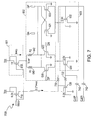
- FIG. 7 is a block diagram of a latch circuit 700 with a bias circuit, in accordance with one embodiment of the present invention.
- the symbols in FIG. 7 that are similar to those in FIG. 6 have similar functions as those in FIG. 6 , and will not be detailed described herein for purposes of clarity.
- the latch circuit 700 can include an exemplary bias circuit formed by a PMOS transistor 710 and a NMOS transistor 720 .
- the bias circuit can provide a bias voltage to control the NMOS transistor 610 .
- the bias circuit in FIG. 7 can further provide complementary clock signals CLKP and CLKN to the third level 603 .
- Resistors 730 and 732 can be used to block AC components from the bias circuit to the NMOS transistors 630 and 632 respectively.
- Capacitors 740 and 742 can be used to block DC components from the pair of complementary clock signals CLKP and CLKN to the NMOS transistors 630 and 632 respectively.
- FIG. 8 is a block diagram of an electronic system 800 , in accordance with one embodiment of the present invention.
- the electronic system 800 can be implemented in, but is not limited to a global positioning system (GPS) receiver, a code division multiple access (CDMA) transceiver, etc.
- the electronic system 800 can include a voltage control oscillator (VCO) 810 and a frequency divider.
- VCO voltage control oscillator
- the frequency divider in FIG. 8 is a divide-by-two circuit (DTC).
- DTC divide-by-two circuit
- the DTC circuit in FIG. 8 can include a first latch circuit 820 and a second latch circuit 830 .
- the first latch circuit 820 is identical to the second latch circuit 830 , in one embodiment.
- the first latch circuit 820 and the second latch circuit 830 can employ the configuration described in FIG. 6 or FIG. 7 and will not be detailed described herein.
- Output signals of the first latch circuit 820 are sent to the second latch circuit 830 as input signals of the second latch circuit 830 .
- output signals of the second latch circuit 830 are sent back to the first latch circuit 820 as input signals of the first latch circuit 820 .
- the frequency of the signals DP 2 and DN 2 is half of the frequency of the clock signals CLKP and CLKN, in one embodiment.
- the VCO 810 can include a PMOS transistor 801 to generate a source current.
- the source current of the VCO 810 can flow through inductors 820 and 822 , capacitors 830 and 832 , and a pair of cross-coupled NMOS transistors 840 and 842 .
- the NMOS transistors 840 and 842 can be equipped with a relatively large size in order to provide enough transconductance of the VCO 810 and provide enough voltage swing of output signals.
- the output signals e.g., the pair of complementary clock signals CLKP and CLKN
- the NMOS transistors 630 and 632 are of a smaller size so that the electronic system 800 can operate in a higher frequency.
- a buffer to provide a higher input voltage swing of the DTC can be saved.
- FIG. 9 is a flowchart 900 of a method for dividing a frequency of an input signal (e.g., the clock signals CLKP and CLKN in FIG. 8 ), in accordance with one embodiment of the present invention.
- FIG. 9 is described in combination with FIG. 6 .
- a source current I PRES is generated by a first transistor (e.g., the PMOS transistor 610 ) having a source terminal and a substrate coupled to a source voltage.
- a second transistor e.g., the NMOS transistor 630
- the second transistor has a source terminal and a substrate coupled to ground.
- a third transistor (e.g., the NMOS transistor 632 ) is controller by a complementary of the clock signal (e.g., by the clock signal CLKN).
- the third transistor has a source terminal and a substrate coupled to ground.
- the second transistor and the third transistor receive the source current alternately under the control of the pair of clock signals CLKP and CLKN.
- a frequency divider that can include the first latch circuit 820 and the second latch circuit 830 coupled to the first latch circuit 820 .
- the second latch circuit 830 can be identical to the first latch circuit 820 .
- the first latch circuit 820 can include the first level 601 , the second level 602 and the third level 603 .
- the first level 601 e.g., the PMOS transistor 610
- the PMOS transistor 610 has the source terminal and the substrate both coupled to the source voltage V DD .
- the second level 602 is coupled between the first level 601 and the third level 603 for receiving a pair of input signals DN and DP and for generating a pair of output signals QN and QP.
- the second level 602 can generate the voltage swing of output signals QN and QP according to the source current I PRES .
- the third level 603 e.g., the NMOS transistors 630 and 632
- the NMOS transistor 630 can receive the source current I PRES via a pair of source-coupled transistors (e.g., the NMOS transistors 620 and 622 ).
- the NMOS transistor 632 can receive the source current I PRES via a pair of cross-coupled transistors (e.g., the NMOS transistors 621 and 623 ).
- the NMOS transistors 630 and 632 are controlled by the pair of clock signals CLKN and CLKP respectively.
- Each of the NMOS transistors 630 and 632 has the source terminal and the substrate both coupled to ground.
Landscapes
- Logic Circuits (AREA)
Abstract
Description
V SWING =V HIGH −V LOW =V DD−(V DD −I PRES *R 1)=I PRES *R 1 (1)
VSWING represents the voltage swing of the output signal QN. VHIGH represents a voltage value of QN when the output signal QN is logic high. VLow represents a voltage value of QN when the output signal QN is logic low. R1 represents the resistance of the
I PRES =V REF /R REF (2)
VREF represents the input reference voltage at the negative terminal of the
V SWING =I PRES *R 1 =V REF*(R 1 /R REF) (3)
V LOW =V CMP −I PRES *R LOAD
RLOAD
VHIGH=VCMP (5)
VHIGH represents the voltage value of QP when the output signal QP is logic high.
V SWING =V HIGH −V LOW =V CMP−(V CMP 31 I PRES*RLOAD
Claims (18)
Priority Applications (2)
| Application Number | Priority Date | Filing Date | Title |
|---|---|---|---|
| US12/156,909 US7750693B2 (en) | 2007-06-05 | 2008-06-05 | Frequency divider including latch circuits |
| TW097120882A TWI350646B (en) | 2007-06-05 | 2008-06-05 | Frequency divider and latch circuit and frequency dividing method thereof |
Applications Claiming Priority (2)
| Application Number | Priority Date | Filing Date | Title |
|---|---|---|---|
| US93339407P | 2007-06-05 | 2007-06-05 | |
| US12/156,909 US7750693B2 (en) | 2007-06-05 | 2008-06-05 | Frequency divider including latch circuits |
Publications (2)
| Publication Number | Publication Date |
|---|---|
| US20080303561A1 US20080303561A1 (en) | 2008-12-11 |
| US7750693B2 true US7750693B2 (en) | 2010-07-06 |
Family
ID=40095300
Family Applications (1)
| Application Number | Title | Priority Date | Filing Date |
|---|---|---|---|
| US12/156,909 Active 2028-08-07 US7750693B2 (en) | 2007-06-05 | 2008-06-05 | Frequency divider including latch circuits |
Country Status (3)
| Country | Link |
|---|---|
| US (1) | US7750693B2 (en) |
| CN (1) | CN101320971B (en) |
| TW (1) | TWI350646B (en) |
Cited By (5)
| Publication number | Priority date | Publication date | Assignee | Title |
|---|---|---|---|---|
| US20100176877A1 (en) * | 2009-01-15 | 2010-07-15 | Fujitsu Limited | Direct-current potential generation circuit, multistage circuit and communication apparatus |
| US20110241789A1 (en) * | 2010-04-01 | 2011-10-06 | National Tsing Hua University (Taiwan) | Integrated circuit capable of repeatedly using current |
| US20120081156A1 (en) * | 2010-09-30 | 2012-04-05 | Leonardus Hesen | High Speed RF Divider |
| US8493105B2 (en) | 2011-10-14 | 2013-07-23 | Industrial Technology Research Institute | Injection-locked frequency divider |
| US9843329B2 (en) * | 2014-05-27 | 2017-12-12 | Nxp B.V. | Multi-modulus frequency divider |
Families Citing this family (9)
| Publication number | Priority date | Publication date | Assignee | Title |
|---|---|---|---|---|
| DE102010029140A1 (en) * | 2010-05-19 | 2011-11-24 | Sensordynamics Ag | Built-in CMOS wide band clock with differential design |
| CN101888245A (en) * | 2010-06-04 | 2010-11-17 | 西安电子科技大学 | GaAs HBT Ultra High Speed Divider by 2 |
| US8456202B2 (en) * | 2011-02-15 | 2013-06-04 | Texas Instruments Incorporated | Latch divider |
| CN103684424B (en) * | 2012-09-20 | 2017-03-01 | 复旦大学 | A kind of wide lock-in range current-mode latch divider based on source-electrode degradation electric capacity |
| TWI508428B (en) * | 2012-11-22 | 2015-11-11 | Ind Tech Res Inst | Current reuse frequency divider and method thereof and voltage control oscillator module and phase lock loop using the same |
| CN103281071B (en) * | 2013-06-21 | 2016-04-13 | 中国科学院上海高等研究院 | Latch and comprise the divider circuit of this latch |
| US9973182B2 (en) * | 2016-09-14 | 2018-05-15 | Qualcomm Incorporated | Re-timing based clock generation and residual sideband (RSB) enhancement circuit |
| US11070200B2 (en) * | 2018-09-27 | 2021-07-20 | Intel Corporation | Duty cycle correction system and low dropout (LDO) regulator based delay-locked loop (DLL) |
| CN110214417B (en) * | 2019-04-18 | 2023-05-02 | 香港应用科技研究院有限公司 | 50% Duty Cycle Quadrature Input Quadrature Output (QIQO) Divide-by-3 Circuit |
Citations (18)
| Publication number | Priority date | Publication date | Assignee | Title |
|---|---|---|---|---|
| US5714394A (en) * | 1996-11-07 | 1998-02-03 | Advanced Micro Devices, Inc. | Method of making an ultra high density NAND gate using a stacked transistor arrangement |
| US5801565A (en) * | 1996-03-07 | 1998-09-01 | National Semiconductor Corporation | High speed differential data latch |
| US5818293A (en) * | 1997-02-26 | 1998-10-06 | Advanced Micro Devices, Inc. | High speed analog flip-flop with embedded logic and phase-locked-loop circuit employing the same |
| US6104214A (en) | 1997-03-25 | 2000-08-15 | Mitsubishi Denki Kabushiki Kaisha | Current mode logic circuit, source follower circuit, and flip flop circuit |
| US6166571A (en) | 1999-08-03 | 2000-12-26 | Lucent Technologies Inc. | High speed frequency divider circuit |
| US6501314B1 (en) * | 2002-03-06 | 2002-12-31 | Teradyne, Inc. | Programmable differential D flip-flop |
| US6762624B2 (en) * | 2002-09-03 | 2004-07-13 | Agilent Technologies, Inc. | Current mode logic family with bias current compensation |
| US6777988B2 (en) | 2002-04-30 | 2004-08-17 | John C. Tung | 2-level series-gated current mode logic with inductive components for high-speed circuits |
| US6831489B2 (en) | 2002-05-21 | 2004-12-14 | The Hong Kong University Of Science And Technology | Low-voltage high-speed frequency-divider circuit |
| US6861888B2 (en) * | 2002-01-16 | 2005-03-01 | Agilent Technologies, Inc. | High-sensitivity differential data latch system |
| US20050110525A1 (en) * | 2003-11-20 | 2005-05-26 | Mitsubishi Denki Kabushiki Kaisha | Current-mode logic circuit |
| US20060145743A1 (en) | 2004-12-03 | 2006-07-06 | Volker Neubauer | Data latch, master/slave flipflop and frequency divider circuit |
| US7154294B2 (en) * | 2005-02-23 | 2006-12-26 | Via Technologies Inc. | Comparators capable of output offset calibration |
| US7233211B2 (en) * | 2004-12-06 | 2007-06-19 | Broadcom Corporation | Method to improve high frequency divider bandwidth coverage |
| US7236029B2 (en) * | 2004-02-26 | 2007-06-26 | Infineon Technologies Ag | Flip-flop circuit arrangement and method for processing a signal |
| US7298183B2 (en) * | 2005-06-01 | 2007-11-20 | Wilinx Corp. | High frequency divider circuits and methods |
| US7429874B2 (en) * | 2005-11-15 | 2008-09-30 | Electronics And Telecommunications Research Institute | Replica bias circuit |
| US7521976B1 (en) * | 2004-12-08 | 2009-04-21 | Nanoamp Solutions, Inc. | Low power high speed latch for a prescaler divider |
-
2008
- 2008-06-05 US US12/156,909 patent/US7750693B2/en active Active
- 2008-06-05 CN CN2008101112066A patent/CN101320971B/en active Active
- 2008-06-05 TW TW097120882A patent/TWI350646B/en not_active IP Right Cessation
Patent Citations (18)
| Publication number | Priority date | Publication date | Assignee | Title |
|---|---|---|---|---|
| US5801565A (en) * | 1996-03-07 | 1998-09-01 | National Semiconductor Corporation | High speed differential data latch |
| US5714394A (en) * | 1996-11-07 | 1998-02-03 | Advanced Micro Devices, Inc. | Method of making an ultra high density NAND gate using a stacked transistor arrangement |
| US5818293A (en) * | 1997-02-26 | 1998-10-06 | Advanced Micro Devices, Inc. | High speed analog flip-flop with embedded logic and phase-locked-loop circuit employing the same |
| US6104214A (en) | 1997-03-25 | 2000-08-15 | Mitsubishi Denki Kabushiki Kaisha | Current mode logic circuit, source follower circuit, and flip flop circuit |
| US6166571A (en) | 1999-08-03 | 2000-12-26 | Lucent Technologies Inc. | High speed frequency divider circuit |
| US6861888B2 (en) * | 2002-01-16 | 2005-03-01 | Agilent Technologies, Inc. | High-sensitivity differential data latch system |
| US6501314B1 (en) * | 2002-03-06 | 2002-12-31 | Teradyne, Inc. | Programmable differential D flip-flop |
| US6777988B2 (en) | 2002-04-30 | 2004-08-17 | John C. Tung | 2-level series-gated current mode logic with inductive components for high-speed circuits |
| US6831489B2 (en) | 2002-05-21 | 2004-12-14 | The Hong Kong University Of Science And Technology | Low-voltage high-speed frequency-divider circuit |
| US6762624B2 (en) * | 2002-09-03 | 2004-07-13 | Agilent Technologies, Inc. | Current mode logic family with bias current compensation |
| US20050110525A1 (en) * | 2003-11-20 | 2005-05-26 | Mitsubishi Denki Kabushiki Kaisha | Current-mode logic circuit |
| US7236029B2 (en) * | 2004-02-26 | 2007-06-26 | Infineon Technologies Ag | Flip-flop circuit arrangement and method for processing a signal |
| US20060145743A1 (en) | 2004-12-03 | 2006-07-06 | Volker Neubauer | Data latch, master/slave flipflop and frequency divider circuit |
| US7233211B2 (en) * | 2004-12-06 | 2007-06-19 | Broadcom Corporation | Method to improve high frequency divider bandwidth coverage |
| US7521976B1 (en) * | 2004-12-08 | 2009-04-21 | Nanoamp Solutions, Inc. | Low power high speed latch for a prescaler divider |
| US7154294B2 (en) * | 2005-02-23 | 2006-12-26 | Via Technologies Inc. | Comparators capable of output offset calibration |
| US7298183B2 (en) * | 2005-06-01 | 2007-11-20 | Wilinx Corp. | High frequency divider circuits and methods |
| US7429874B2 (en) * | 2005-11-15 | 2008-09-30 | Electronics And Telecommunications Research Institute | Replica bias circuit |
Non-Patent Citations (3)
| Title |
|---|
| "Design of Analog CMOS Integrated Circuits", Chapter 2.3, Body Effect, Behzad Razavi (p. 23-p. 28, 6 pages). |
| "RF Microelectronic", Chapter 8.4, Frequency Divider, Behzad Razavi (Pate 290-Pate 296, 6 pates). |
| "The Impact of Device Type and Sizing on Phase Noise Mechanisms", IEEE Journal of Solid State Circuits, vol. 40, No. 2, Feb. 2005 (Pate 360-p. 369, 10 pages). |
Cited By (6)
| Publication number | Priority date | Publication date | Assignee | Title |
|---|---|---|---|---|
| US20100176877A1 (en) * | 2009-01-15 | 2010-07-15 | Fujitsu Limited | Direct-current potential generation circuit, multistage circuit and communication apparatus |
| US20110241789A1 (en) * | 2010-04-01 | 2011-10-06 | National Tsing Hua University (Taiwan) | Integrated circuit capable of repeatedly using current |
| US20120081156A1 (en) * | 2010-09-30 | 2012-04-05 | Leonardus Hesen | High Speed RF Divider |
| US8487669B2 (en) * | 2010-09-30 | 2013-07-16 | St-Ericsson Sa | High speed RF divider |
| US8493105B2 (en) | 2011-10-14 | 2013-07-23 | Industrial Technology Research Institute | Injection-locked frequency divider |
| US9843329B2 (en) * | 2014-05-27 | 2017-12-12 | Nxp B.V. | Multi-modulus frequency divider |
Also Published As
| Publication number | Publication date |
|---|---|
| TW200913461A (en) | 2009-03-16 |
| US20080303561A1 (en) | 2008-12-11 |
| CN101320971B (en) | 2010-07-07 |
| TWI350646B (en) | 2011-10-11 |
| CN101320971A (en) | 2008-12-10 |
Similar Documents
| Publication | Publication Date | Title |
|---|---|---|
| US7750693B2 (en) | Frequency divider including latch circuits | |
| US7589583B2 (en) | Charge pump circuit | |
| US7920012B2 (en) | Semiconductor device | |
| CN113890334B (en) | Voltage multiplier circuit for generating positive and negative voltages | |
| US8456225B1 (en) | Negative charge pump | |
| US7576613B2 (en) | Regulated cascode circuits and CMOS analog circuits including the same | |
| US20070164812A1 (en) | High voltage tolerant bias circuit with low voltage transistors | |
| US7221190B2 (en) | Differential comparator with extended common mode voltage range | |
| JP2008211707A (en) | Input circuit | |
| US7268623B2 (en) | Low voltage differential signal driver circuit and method for controlling the same | |
| US7236002B2 (en) | Digital CMOS-input with N-channel extended drain transistor for high-voltage protection | |
| US7449940B2 (en) | Buffer circuit | |
| US12481302B2 (en) | Constant voltage circuit | |
| EP3614564B1 (en) | Charge pump circuit with capacitor swapping technique and associated method | |
| CN117648016A (en) | Source switching charge pumps and phase locked loops for low temperature applications | |
| KR20120097830A (en) | Temperature compensation circuit and device for comprising the same | |
| EP4002690B1 (en) | Delay circuit | |
| US7652524B2 (en) | Voltage source for gate oxide protection | |
| US20040130348A1 (en) | Semiconductor integrated circuit having a plurality of threshold voltages | |
| US10116261B2 (en) | Oscillator circuit | |
| US7498892B2 (en) | Split-biased interpolated voltage-controlled oscillator and phase locked loop | |
| JP2024042582A (en) | Analog switch circuit, semiconductor device | |
| JP3767697B2 (en) | Semiconductor integrated circuit device | |
| JP4134160B2 (en) | Semiconductor integrated circuit device | |
| US9088254B2 (en) | Differential-to-single-end converter |
Legal Events
| Date | Code | Title | Description |
|---|---|---|---|
| AS | Assignment |
Owner name: O2MICRO INC., CALIFORNIA Free format text: ASSIGNMENT OF ASSIGNORS INTEREST;ASSIGNORS:CHU, MENG;TAN, SEETECK;REEL/FRAME:021115/0228 Effective date: 20080604 |
|
| STCF | Information on status: patent grant |
Free format text: PATENTED CASE |
|
| AS | Assignment |
Owner name: O2MICRO INTERNATIONAL LIMITED., CAYMAN ISLANDS Free format text: ASSIGNMENT OF ASSIGNORS INTEREST;ASSIGNOR:O2MICRO, INC.;REEL/FRAME:024894/0276 Effective date: 20100820 |
|
| AS | Assignment |
Owner name: MAISHI ELECTRONIC (SHANGHAI) LTD, CHINA Free format text: ASSIGNMENT OF ASSIGNORS INTEREST;ASSIGNOR:O2MICRO INTERNATIONAL LIMITED;REEL/FRAME:029273/0818 Effective date: 20121106 |
|
| FPAY | Fee payment |
Year of fee payment: 4 |
|
| FEPP | Fee payment procedure |
Free format text: ENTITY STATUS SET TO SMALL (ORIGINAL EVENT CODE: SMAL) |
|
| MAFP | Maintenance fee payment |
Free format text: PAYMENT OF MAINTENANCE FEE, 8TH YR, SMALL ENTITY (ORIGINAL EVENT CODE: M2552) Year of fee payment: 8 |
|
| MAFP | Maintenance fee payment |
Free format text: PAYMENT OF MAINTENANCE FEE, 12TH YR, SMALL ENTITY (ORIGINAL EVENT CODE: M2553); ENTITY STATUS OF PATENT OWNER: SMALL ENTITY Year of fee payment: 12 |
|
| AS | Assignment |
Owner name: O2MICRO INTERNATIONAL LTD., CAYMAN ISLANDS Free format text: ASSIGNMENT OF ASSIGNORS INTEREST;ASSIGNOR:MAISHI ELECTRONIC (SHANGHAI) CO., LTD.;REEL/FRAME:058612/0041 Effective date: 20211220 |