US7746262B2 - Coding method for digital to analog converter of a SAR analog to digital converter - Google Patents
Coding method for digital to analog converter of a SAR analog to digital converter Download PDFInfo
- Publication number
- US7746262B2 US7746262B2 US11/311,509 US31150905A US7746262B2 US 7746262 B2 US7746262 B2 US 7746262B2 US 31150905 A US31150905 A US 31150905A US 7746262 B2 US7746262 B2 US 7746262B2
- Authority
- US
- United States
- Prior art keywords
- bit
- value
- bits
- ground
- reference voltage
- Prior art date
- Legal status (The legal status is an assumption and is not a legal conclusion. Google has not performed a legal analysis and makes no representation as to the accuracy of the status listed.)
- Active, expires
Links
- 238000000034 method Methods 0.000 title claims abstract description 66
- 239000003990 capacitor Substances 0.000 claims abstract description 172
- 238000006243 chemical reaction Methods 0.000 claims description 17
- 238000005070 sampling Methods 0.000 claims description 17
- 230000001052 transient effect Effects 0.000 claims description 6
- 238000012360 testing method Methods 0.000 description 52
- 238000010586 diagram Methods 0.000 description 7
- 238000003491 array Methods 0.000 description 2
- 230000004075 alteration Effects 0.000 description 1
- 230000003247 decreasing effect Effects 0.000 description 1
- 239000002184 metal Substances 0.000 description 1
- 238000006467 substitution reaction Methods 0.000 description 1
Images


Classifications
-
- H—ELECTRICITY
- H03—ELECTRONIC CIRCUITRY
- H03M—CODING; DECODING; CODE CONVERSION IN GENERAL
- H03M1/00—Analogue/digital conversion; Digital/analogue conversion
- H03M1/12—Analogue/digital converters
- H03M1/34—Analogue value compared with reference values
- H03M1/38—Analogue value compared with reference values sequentially only, e.g. successive approximation type
- H03M1/46—Analogue value compared with reference values sequentially only, e.g. successive approximation type with digital/analogue converter for supplying reference values to converter
- H03M1/462—Details of the control circuitry, e.g. of the successive approximation register
-
- H—ELECTRICITY
- H03—ELECTRONIC CIRCUITRY
- H03M—CODING; DECODING; CODE CONVERSION IN GENERAL
- H03M1/00—Analogue/digital conversion; Digital/analogue conversion
- H03M1/12—Analogue/digital converters
- H03M1/34—Analogue value compared with reference values
- H03M1/38—Analogue value compared with reference values sequentially only, e.g. successive approximation type
- H03M1/46—Analogue value compared with reference values sequentially only, e.g. successive approximation type with digital/analogue converter for supplying reference values to converter
- H03M1/466—Analogue value compared with reference values sequentially only, e.g. successive approximation type with digital/analogue converter for supplying reference values to converter using switched capacitors
- H03M1/468—Analogue value compared with reference values sequentially only, e.g. successive approximation type with digital/analogue converter for supplying reference values to converter using switched capacitors in which the input S/H circuit is merged with the feedback DAC array
-
- H—ELECTRICITY
- H03—ELECTRONIC CIRCUITRY
- H03M—CODING; DECODING; CODE CONVERSION IN GENERAL
- H03M1/00—Analogue/digital conversion; Digital/analogue conversion
- H03M1/66—Digital/analogue converters
- H03M1/68—Digital/analogue converters with conversions of different sensitivity, i.e. one conversion relating to the more significant digital bits and another conversion to the less significant bits
- H03M1/682—Digital/analogue converters with conversions of different sensitivity, i.e. one conversion relating to the more significant digital bits and another conversion to the less significant bits both converters being of the unary decoded type
-
- H—ELECTRICITY
- H03—ELECTRONIC CIRCUITRY
- H03M—CODING; DECODING; CODE CONVERSION IN GENERAL
- H03M1/00—Analogue/digital conversion; Digital/analogue conversion
- H03M1/66—Digital/analogue converters
- H03M1/68—Digital/analogue converters with conversions of different sensitivity, i.e. one conversion relating to the more significant digital bits and another conversion to the less significant bits
- H03M1/687—Segmented, i.e. the more significant bit converter being of the unary decoded type and the less significant bit converter being of the binary weighted type
Definitions
- the present invention relates to digital to analog converters, and more particularly, to successive approximation registers.
- a successive approximation register comprises an analog to digital conversion method in which the input voltage is compared with the output voltage of a sequentially programmed digital to analog converter.
- MSB most significant bit
- the MSB is turned on and compared with an analog input voltage. If the input voltage is greater than the digital to analog output, the MSB is left at logic high. Otherwise, the MSB is turned to logic low. This process is repeated for all other bits in decreasing order until the least significant bit (LSB) is reached.
- a very popular digital to analog converter architecture used in CMOS technology is the charge scaling DAC.
- a 10-bit split array binary weighted (binary coded) DAC includes capacitors on both sides of a bridge capacitor that are binary weighted.
- a capacitance value C is the unit capacitor of any value.
- This DAC architecture is widely used in charge distribution ADCs.
- the capacitor array itself is the critical component of the ADC because of the need for precisely/accurately ratioed capacitors.
- the linearity of the ADC depends on the matching between the ratios of the capacitors associated with the bits of the array. As the number of bits increases, the ratio of the MSB capacitor to the LSB capacitor becomes more difficult to control.
- the ratio mismatches between the capacitors are greatly reduced by building each capacitor out of the unit capacitor C and by using special layout techniques. Yet there is a great need to further improve the matching of the capacitor ratios, especially with an increase in the number of bits.
- capacitor calibration techniques are used to achieve better matching between the capacitors. However, this technique would require additional calibration circuits.
- the comparators used within some types of SAR ADC circuits have large transients applied to their inputs using existing coding techniques. As long as these transients settle down within the time allowed for the comparison by the comparator, this is not a problem. However, for ADCs with higher resolution and speed, the larger transients may place a limitation on the settling times of the input mode of the comparator. Thus, there's a need to improve the operation of SAR analog to digital converters within a digital to analog converter with smaller transients for higher resolution comparators and some method for improving the matching between capacitors without requiring additional calibration circuits.
- FIG. 1 is a functional block diagram of a successive approximation A/D converter
- FIG. 2 illustrates a 10 bit split array binary weighted digital to analog converter used within a SAR A/D converter
- FIG. 3 is a flow diagram illustrating the operation of the digital to analog converter of FIG. 2 using a prior art control method
- FIG. 4 illustrates the unit capacitors and control switches necessary to operate the first two bits of the digital to analog controller of FIG. 2 according to the control method of the present disclosure
- FIG. 5 a is a flow diagram illustrating the operation of an SAR ADC on the MSB side using a thermometer coding technique
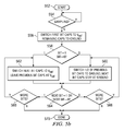
- FIG. 5 b is a simplified flow chart of the process of FIG. 5 a;
- FIG. 6 illustrates a 10 bit split array digital to analog converter wherein a first three most significant bits are thermometer coded and the remaining bits are binary coded;
- FIG. 7 is a flow chart illustrating the SAR bit decision making process of the three MSBs utilizing fully thermometer coding technique of FIG. 6 .
- the present invention disclosed and claimed herein in one aspect thereof, comprises a method for coding a successive approximation register.
- the process includes the steps of switching capacitors associated with a bit from ground to a reference voltage. Next, a determination is made whether a logical value of the bit is a first value or a second value. If the logical value of the bit is the first value, capacitors associated with the next bit are switched from ground to the reference voltage. If the logical value of the bit is the second value, one-half of the capacitors associated with the bit currently connected to the reference voltage are switched to ground.
- Successive approximation A/D conversion is a technique that is commonly used in medium to high speed data acquisition applications.
- the successive approximation A/D conversion is one of the fastest A/D conversion techniques that requires a minimum amount of circuitry.
- the successive approximation A/D converter can approximate the analog to digital signal to form an n bit digital code in n steps.
- the successive approximation register 102 individually compares an analog input voltage to the mid point of one of n ranges to determine the value of one bit. This process is repeated a total n times, using n ranges, to determine the n bits of the code. The comparison is accomplished as follows.
- the SAR 102 determines if the analog input is above or below the midpoint and sets the bit of the digital code accordingly.
- the SAR 102 assigns the bits beginning with the most significant bit. The bit is set to “1” if the analog input is greater than the midpoint voltage, or it is set at “0” if it is less than the midpoint voltage.
- the SAR 102 then moves to the next bit and sets it as a “1” or a “0” based on the results of comparing the analog input with a midpoint of the next allowed range. Because the SAR must perform one approximation for each bit in the digital code, an n bit code requires n approximations.
- the success of approximation A/D converter as illustrated in FIG. 1 consists of four functional blocks.
- Location to the n bit approximation is controlled by the control shift register 110 .
- the output latch 112 latches in the bits of the digital output code as they are determined by the SAR 102 .
- Analog comparator 104 performs the comparisons of an analog input voltage with the midpoint of the selected one of n ranges presently being examined.
- the 10 bit split array binary weighted DAC 202 consists of a group of capacitors 204 connected in parallel wherein a first plate of each capacitor is interconnected at a common node 206 , and a second group of capacitors 208 connected in parallel wherein a first plate of each of these capacitors 208 is connected to a second common node 210 .
- the first node 206 and the second node 210 are interconnected via a bridge capacitor 212 .
- the capacitors 204 and 208 are binary weighted capacitors that progressively double in their capacitance from bit 0 -bit 4 and from bit 5 -bit 9 .
- the capacitance of bit 0 is C
- the capacitance of bit 1 is 2C
- the capacitive of bit 2 is 4C and so on until the capacitance of the bit 4 is equal to 16C.
- the opposite plates of capacitors 204 or 208 which are not connected with common nodes 206 and 210 , respectively, are selectively connected to either of an input voltage V in through switch 214 , a reference voltage V ref through switch 216 or ground through a switch 218 .
- the capacitors connected to common node 206 comprise the most significant bits (MSBs) of the DAC 210
- the capacitors connected to the node 210 comprise the least significant bits (LSBs).
- a dummy capacitor 220 connects between node 210 and ground.
- Node 206 is connected to a negative input of comparator 222 .
- the positive input of capacitor 222 is connected to ground or some dc common-mode voltage.
- a change of logical state of the output of comparator 222 indicates that the bit being tested should be logical “1”. If the output of the comparator remains constrained the bit being listed is logical “0.”
- the comparator's output state flips and the decision is made to keep the MSB to the logic high (logic “1”) state and its capacitor remains connected to the reference voltage.
- the next (MSB-1 bit) bit, bit- 8 is then tested by switching its caps from ground to the reference voltage. However, if the comparator's 222 output state does not flip at the end of the MSB test, the MSB is set to logic “0”, and the MSB-1 bit (bit- 8 ) test proceeds by switching all of the MSB caps from reference to ground, and by switching all MSB-1 caps (8C) from ground to reference voltage.
- step 302 determines whether the SAR is within a sampling mode.
- Inquiry step 304 continues to monitor while the SAR is determined to be within the sampling mode.
- the most significant bit capacitor is switched to the reference voltage V ref at step 306 while the remaining capacitors for the other bits are switched to ground.
- Inquiry step 308 determines if the most significant bit (MSB) should be set equal to logical “1” or logical “0” depending upon the output of the comparator 222 .
- the capacitors for the next bit are switched to the reference voltage V ref , and the capacitors of the previously tested bit are switched to ground at step 310 .
- the capacitors of the remaining bits remain connected to ground.
- the MSB bit is set to logical “1”
- the capacitors of the next bit are switched to the reference voltage V ref while the capacitors of the previous bit remain at the reference voltage at step 312 .
- the capacitors of the remaining bits remain connected to ground.
- inquiry step 314 determines whether the newly tested bit should be set to a logical “1” or a logical “0” based upon the output of the comparator 222 . If the bit is set to logical “0”, control passes to inquiry step 316 , which determines whether there are further bits to be tested. If so, control passes back to step 310 . Otherwise, the process is completed at step 320 . If the tested bit is determined to be set to logical “1” at inquiry step 314 , inquiry step 318 determines if there are further bits to be tested, and if so, control passes back to step 312 . If no other bits are available for testing, the process is completed at step 320 .
- One manner for combating this problem is more fully illustrated with respect to FIG. 4 .
- One way for overcoming this issue is enabled by using multiple unit capacitors C for each capacitor having a value of multiple unit capacitors C.
- multiple capacitors are used as illustrated in FIG. 4 .
- the MSB bit 9
- the MSB would comprise 16 separate capacitors 402 each having a value of C.
- Each of these capacitors 402 would be connected to a separate switch array 404 including three switches alternately connecting the capacitor 402 to the input voltage V in , the reference voltage V ref and ground.
- bit 8 rather than including a single capacitor having a value of 8C would include eight separate capacitors 406 . Each of these eight capacitors have a value C, and each of these capacitors are connected to a switching array 404 connecting the capacitor to either the input voltage V in , the reference voltage V ref or ground.
- bit- 7 of the SAR DAC would include four separate capacitors having a value of C wherein each of the capacitors are connected to a switch array 404 .
- Bit- 6 would include two capacitors each having a value of C and each capacitor connected to a switch array 404
- bit- 5 would include a single capacitor 204 having a value of C and connected to a switch array 404 .
- the 5-bits (bit- 4 thru bit- 0 ) making up the least significant bits would be similarly configured to the MSB bits.
- the coding of the SAR DAC 202 may be altered such that testing does not necessarily move to a next most significant bit capacitor when a previous bit's capacitors has been determined to be at a logic low (logic “0”) value.
- the capacitors associated with a next bit will remain switched to ground, and half of the unit capacitors of the previously tested bit that are connected to the reference voltage are switched to ground. The remaining half of the capacitors associated with the previously tested bit stay connected to the reference voltage V ref .
- the weight of the capacitor of the presently tested bit is one-half of the weight of the capacitor of the previously tested bit.
- the total transient perturbation on the input node of the comparator 222 will be greatly reduced since only a single group of switches are switched, and capacitor matching will be better because half of the capacitors within the previously tested capacitor will be used to decide the state of the next bit.
- FIG. 5 a there is illustrated a diagram showing the bit decision making process for the MSB side of a fully thermometer coded 10-bit SAR ADC.
- This figure illustrates the operation for determining the logical values for bit- 9 through bit- 5 (the MSB bits). The determination of the logical values for bit- 4 through bit- 0 will occur in the exact same manner for the least significant bits.
- a determination is made if the ADC is in a sampling mode or a conversion mode. If the determination is made that the ADC is in the sampling mode, the process continues to monitor until the device enters the conversion mode.
- step 504 determines the conversion mode has been entered.
- step 504 determines the conversion mode has been entered.
- step 504 a test is performed on the MSB bit.
- the capacitors for the MSB bit are switched to the reference voltage V ref .
- the capacitors of the remaining bits are switched to ground.
- the capacitors for the MSB-1 bit are all switched from ground to the reference voltage V ref .
- the capacitors for the MSB bit remain connected to the reference voltage V ref since the MSB bit has been set to logic “1”.
- the output of the comparator is monitored at node 514 to determine whether the MSB-1 bit should be set to logic “1” or logic “0”.
- Step 516 there is described the process for performing a test on the MSB-2 bit, when both the MSB bit and the MSB-1 bit are set to logic “0”. If this occurs, the test on the MSB-2 bit is performed by maintaining one-fourth of the capacitors of the MSB bit at the voltage reference V ref . Since in this case, one-half of the capacitors of the MSB bit were already connected to V ref for the previous test on the MSB-1 bit only one-half of the remaining connected capacitors must be switched from V ref to ground. The output of the comparator is monitored at node 518 to determine whether the MSB-2 bit should be set to logic “0” or logic “1”. If the MSB-1 bit was set equal to logic “1”, control passes to step 520 .
- the MSB-2 test is performed by switching all of the MSB-2 capacitors from ground to the reference voltage V ref .
- the output of the comparator is monitored at inquiry node 522 to determine whether the MSB-2 bit is to be set to logic “1” or logic “0”. If the MSB-1 bit was set to logic “0” after the MSB has been set to logic “1”, control passes to step 524 .
- the MSB-2 test is performed at this step by switching half of the capacitors of the MSB-1 bit from the reference voltage V ref to ground. The remaining half of the MSB-1 capacitors are still connected to the reference voltage V ref .
- the output of the comparator is monitored at node 526 to determine if the MSB-2 node should be set to logic “0” or to logic “1”.
- the decisions made at inquiry nodes 518 , 522 and 526 set the stage for determining the value of the MSB-3 bit. If the MSB-2 bit has been set to logic “0” at node 518 , the MSB-3 test is performed at step 528 . At step 528 , the MSB-3 test is performed by keeping one-eighth of the MSB capacitors connected to the reference voltage V ref . Since the previous test was performed by connecting only one quarter of the MSB capacitors to V ref , the test for the MSB-3 test is performed by maintaining one-eighth of the MSB capacitors at V ref and switching the other one-eighth of the capacitors to ground.
- Inquiry node 530 is monitored to determine whether to set the MSB-3 bit at logic “0” or logic “1” based upon the output of the comparator. If the MSB-2 bit is set to logic “1” at any of inquiry nodes 518 , 522 or 526 , the MSB-3 test is performed at step 532 . In this test, all of the capacitors for the MSB-3 bit are switched from ground to V ref . The output of the comparator is monitored at inquiry step 534 to determine whether the MSB-3 bit is to be set to logic “1” or logic “0”. If the MSB-2 bit is set to logic-0 at inquiry node 522 , the MSB-3 test is performed at step 536 .
- Inquiry node 542 monitors the output of the comparator to determine whether the MSB-3 bit is to be set to logical “0” or logical “1”.
- a test will be performed to determine the logic value of the MSB-4 test. If the MSB-3 bit has been set to logic “1” at any of inquiry steps 530 , 534 , 538 or 542 , the MSB-4 test is performed at step 544 . In this step, the capacitors for the MSB-4 bit are all switched from ground to the reference voltage V ref . If inquiry step 530 determines that the MSB-3 bit is set to logical “0”, the MSB-4 test is performed at step 546 . At step 546 , one-sixteenth of the capacitors of the MSB bit remain connected to the reference voltage V ref .
- the MSB-4 test is performed at step 548 . In this test, one-half of the capacitors of the MSB-3 bit are connected to ground and the remaining half of the MSB-3 bits connected to the reference voltage V ref . If inquiry step 538 determines that the MSB-3 bit is equal to logical “0”, the MSB-4 test is performed at step 550 . In this test, three-quarters of the MSB-2 capacitors are connected to ground and one-quarter of the MSB-2 capacitors are connected to the reference voltage V ref .
- step 342 determines that the MSB-3 bit is equal to logical “0”
- the MSB-4 test is performed at step 552 .
- the output of the comparator is examined to determine whether to set the MSB-4 bit to a logical “1” or logical “0” level.
- thermometer coded SAR determines whether the thermometer coded SAR is presently within a sampling mode. If so, the process continues to monitor at inquiry step 554 until it is determined that the SAR is no longer within the sampling mode and is in a conversion mode. Once the SAR enters the conversion mode, the capacitors of a first bit to be tested are switched to V ref at step 556 . The remaining capacitors being tested are connected to ground. Inquiry step 558 determines from the output of the comparator whether the bit being tested should be set to logical “1” or logical “0”.
- step 560 If the bit is set to logical “1”, the capacitors of the next bit to be tested are switched to the reference voltage V ref and the capacitors of the bit previously tested remain connected to the referenced voltage V ref . If the bit is set to logical “0”, control passes to step 560 wherein half of the capacitors of the previously tested bit that are presently connected to V ref are switched to ground. The remaining capacitors remain connected to the reference voltage V ref . The capacitors of the next bit, whose logical value is actually being determined, remain at ground. Inquiry step 564 determines from the output of the comparator, if the logical value of the next bit should be set to logical “1” or logical “0”.
- all of the capacitors are connected to the input voltage V in .
- the SAR decision process begins with the MSB test first with all MSB caps (all 16 unit caps, 4 groups of caps, each group having 4 unit caps) connected to the reference voltage and all other caps connected to ground.
- the capacitor arrays for the MSBs 602 and the LSBs 604 are each connected to the negative input of a comparator 606 .
- the positive input of the comparator 606 is connected to ground or to a dc common-mode.
- the output of the comparator 606 provides the results of each test associated with one of the bits of the code forming the output of the split array DAC.
- the MSB (bit- 9 ) bit, MSB-1 (bit 8 ) bit and MSB-2 (bit 7 ) bit include capacitor groups 608 connected to a common node 610 . Each of the capacitor groups 608 are connected to three switches.
- a first switch 612 connects the capacitor to the input voltage V in .
- a second switch 614 connects the capacitor group 608 to a reference voltage V ref and a third capacitor 616 connects the capacitor group 608 to ground.
- the remaining bits, bit- 6 through bit- 0 are configured with binary coded capacitors 618 .
- the binary coded capacitors 618 for bit- 6 and bit- 5 have a first plate connected to the common node 610 and their other plates connected to the input voltage, reference voltage and ground through switches 612 , 614 and 616 , respectively.
- a bridge capacitor 620 interconnects common node 610 to common node 622 .
- the least significant bits 604 are each formed of binary weighted capacitors 618 for bit- 4 through bit- 0 .
- Each of the least significant bit capacitors have a first plate connected to common node 622 , and a second plate connected to one of the input voltage, the reference voltage and ground via switches 612 , 614 and 616 , respectively.
- step 702 a determination is made if the ADC is in the sampling mode or the convert mode. If the device is in the sampling mode, inquiry step 702 continues to monitor until the conversion mode is detected. Once the conversion mode is detected, a most significant bit test is performed on bit- 9 at step 704 . The capacitors of bit- 9 are all switched to the reference voltage V ref , while the remaining capacitors in the SAR device are connected to ground. The output of the comparator 606 is monitored to determine if the MSB should be set to logic “0” or logic “1”. As described previously, the MSB is set to logic “0” if the state of the output of the comparator does not change states. If the state of the output of the comparator changes, the MSB is set to logic “1”.
- step 708 If the MSB is set to logic “0”, control passes to step 708 , wherein the MSB-1 test is performed by switching half of the capacitors of the MSB (bit- 9 ) to ground and maintaining the remainder of the MSB capacitors at V ref .
- the output of the comparator 606 is monitored to determine whether the MSB-1 bit should be set to logical “0” or logical “1”. If it is determined that the MSB is set to logical “1”, step 712 performs the MSB-1 test by switching the capacitors of the MSB-1 bit (bit- 8 ) from ground to V ref . Since the MSB was set to logical “1”, the capacitors of the MSB remain at V ref .
- the output of the comparator 606 is monitored to determine if the MSB-1 bit should be set to logical “1” or logical “0”.
- step 716 If it is determined at either of inquiry nodes 710 or 714 , that the MSB-1 bit is set to logical “1”, control passes to step 716 , and the MSB-2 test is performed by switching the capacitors of the MSB-2 bit (bit- 7 ) from ground to the reference voltage V ref . If the MSB-1 bit (bit- 8 ) is set to logic “0” at node 710 , step 718 performs the MSB-2 test by switching one-fourth of the capacitors of the MSB bit (bit- 9 ) to ground. Thus, only one-fourth of the capacitors of the MSB remain at the reference voltage V ref .
- the MSB-2 test is performed at step 720 .
- one-half of the capacitors of the MSB-1 bit (bit- 8 ) are switched to ground and the remaining half of the capacitors stay connected to the reference voltage V ref .
- the output of the comparator 606 is monitored to determine the value of bit- 7 . Once a logical value has been assigned to bit 7 , the remainder of bits 6 through bits 0 are assigned using the binary weighted coding technique as described previously herein.
- An n-bit SAR analog to digital converter requires only n-clock cycles to complete all n conversions. Each bit is tested with a control signal, having a time period equal to 1:00. Each test bit issues to a switch of a capacitor associated with the bit under test.
- a control signal having a time period equal to 1:00.
- Each test bit issues to a switch of a capacitor associated with the bit under test.
- the upper three MSB control bits are translated to generate 7 thermometer coded control bits to use for the seven thermometer weighted capacitors to decide the upper three MSB bits 9 - 7 .
- this implementation first iterates the first SAR control signals, the lowest of them are used straight to test the lower SAR bits and the upper three SAR control signals are translated to generate seven thermometer control weighted signals for the seven thermometer weighted caps for the three most significant bits 9 - 7 .
- the transient issues described hereinabove would be significantly reduced as only a single switch is being operated with respect to each particular decision rather than two sets of switching events generating transients to the input of the comparators. Also better matching between the capacitors will be achieved as many a time part of the previously tested capacitors will be used to test the next bit.
Landscapes
- Engineering & Computer Science (AREA)
- Theoretical Computer Science (AREA)
- Analogue/Digital Conversion (AREA)
Abstract
Description
Claims (19)
Priority Applications (1)
| Application Number | Priority Date | Filing Date | Title |
|---|---|---|---|
| US11/311,509 US7746262B2 (en) | 2005-12-19 | 2005-12-19 | Coding method for digital to analog converter of a SAR analog to digital converter |
Applications Claiming Priority (1)
| Application Number | Priority Date | Filing Date | Title |
|---|---|---|---|
| US11/311,509 US7746262B2 (en) | 2005-12-19 | 2005-12-19 | Coding method for digital to analog converter of a SAR analog to digital converter |
Publications (2)
| Publication Number | Publication Date |
|---|---|
| US20070139243A1 US20070139243A1 (en) | 2007-06-21 |
| US7746262B2 true US7746262B2 (en) | 2010-06-29 |
Family
ID=38172800
Family Applications (1)
| Application Number | Title | Priority Date | Filing Date |
|---|---|---|---|
| US11/311,509 Active 2029-02-16 US7746262B2 (en) | 2005-12-19 | 2005-12-19 | Coding method for digital to analog converter of a SAR analog to digital converter |
Country Status (1)
| Country | Link |
|---|---|
| US (1) | US7746262B2 (en) |
Cited By (7)
| Publication number | Priority date | Publication date | Assignee | Title |
|---|---|---|---|---|
| US20120133346A1 (en) * | 2010-11-29 | 2012-05-31 | Kabushiki Kaisha Toshiba | Successive approximation register a/d converter and dc/dc converter |
| US20120326900A1 (en) * | 2011-06-24 | 2012-12-27 | Mediatek Inc. | Successive approximation register analog to digital converter and conversion method thereof |
| US20140232576A1 (en) * | 2013-02-21 | 2014-08-21 | Postech Academy-Industry Foundation | Method and apparatus for calibrating digital background through capacitor division and swapping for reducing capacitor mismatch effect of analog-to-digital converter |
| US9654131B1 (en) * | 2016-02-26 | 2017-05-16 | Texas Instruments Deutschland Gmbh | Capacitor order determination in an analog-to-digital converter |
| US9742423B1 (en) | 2016-10-31 | 2017-08-22 | Silicon Laboratories Inc | Separating most significant bits and least significant bits in charge storage elements of an analog-to-digital converter |
| US9780804B1 (en) * | 2016-06-30 | 2017-10-03 | Synaptics Incorporated | Successive approximation register analog to digital converter with multiple split digital to analog convertors |
| US9831889B1 (en) * | 2016-10-31 | 2017-11-28 | Silicon Laboratories Inc. | Converting large input analog signals in an analog-to-digital converter without input attenuation |
Families Citing this family (15)
| Publication number | Priority date | Publication date | Assignee | Title |
|---|---|---|---|---|
| DE102007033689B4 (en) * | 2007-07-19 | 2009-03-19 | Texas Instruments Deutschland Gmbh | Analog-to-digital converter with successive approximation register and large input range |
| ATE491264T1 (en) | 2007-10-25 | 2010-12-15 | Stichting Imec Nederland | ANALOG-DIGITAL CONVERTER AND METHOD OF USE THEREOF |
| US7898453B2 (en) * | 2008-12-05 | 2011-03-01 | Qualcomm Incorporated | Apparatus and method for successive approximation analog-to-digital conversion |
| CN101800549B (en) * | 2009-02-09 | 2013-04-10 | 义隆电子股份有限公司 | Analog-to-digital converter capable of switching bit resolution and control method thereof |
| US8477052B2 (en) * | 2011-04-05 | 2013-07-02 | Freescale Semiconductor, Inc. | Method and apparatus for self-test of successive approximation register (SAR) A/D converter |
| US20130002468A1 (en) * | 2011-06-28 | 2013-01-03 | International Business Machines Corporation | Analog-digital converter |
| KR101973189B1 (en) * | 2013-04-01 | 2019-04-26 | 에스케이하이닉스 주식회사 | Analog to digital converter, image sensor and method for converting analog to digital |
| DE102014200624B3 (en) * | 2014-01-15 | 2015-03-12 | Fraunhofer-Gesellschaft zur Förderung der angewandten Forschung e.V. | Digital-to-analog converters, analog-to-digital converters and methods of calibrating a digital-to-analog converter |
| JP6287433B2 (en) * | 2014-03-25 | 2018-03-07 | セイコーエプソン株式会社 | Successive comparison type analog-digital converter, physical quantity detection sensor, electronic device and moving body, and successive comparison type analog-digital conversion method |
| KR102339900B1 (en) * | 2015-04-20 | 2021-12-16 | 삼성전자주식회사 | Semiconductor device comprising Successive Approximation Registor Analog to Digital Converter with variable sampling capacitor |
| US9722624B2 (en) * | 2015-04-20 | 2017-08-01 | Samsung Electronics Co., Ltd | Semiconductor device comprising successive approximation register analog to digital converter with variable sampling capacitor |
| US10025423B2 (en) * | 2016-04-25 | 2018-07-17 | Atmel Corporation | Driven shield control |
| WO2018213992A1 (en) * | 2017-05-22 | 2018-11-29 | 深圳市汇顶科技股份有限公司 | Capacitive successive approximation analogue-to-digital converter |
| US10523228B1 (en) * | 2018-12-18 | 2019-12-31 | Ipgreat Incorporated | Method of capacitive DAC calibration for SAR ADC |
| CN112332849B (en) * | 2020-11-11 | 2022-03-29 | 电子科技大学 | Digital-to-analog converter and analog-to-digital converter for realizing low power consumption and low noise |
Citations (1)
| Publication number | Priority date | Publication date | Assignee | Title |
|---|---|---|---|---|
| US20060232461A1 (en) * | 2005-04-13 | 2006-10-19 | Felder Matthew D | Successive approximation analog-to-digital converter with current steered digital-to-analog converter |
-
2005
- 2005-12-19 US US11/311,509 patent/US7746262B2/en active Active
Patent Citations (1)
| Publication number | Priority date | Publication date | Assignee | Title |
|---|---|---|---|---|
| US20060232461A1 (en) * | 2005-04-13 | 2006-10-19 | Felder Matthew D | Successive approximation analog-to-digital converter with current steered digital-to-analog converter |
Cited By (11)
| Publication number | Priority date | Publication date | Assignee | Title |
|---|---|---|---|---|
| US20120133346A1 (en) * | 2010-11-29 | 2012-05-31 | Kabushiki Kaisha Toshiba | Successive approximation register a/d converter and dc/dc converter |
| US20120326900A1 (en) * | 2011-06-24 | 2012-12-27 | Mediatek Inc. | Successive approximation register analog to digital converter and conversion method thereof |
| US8508400B2 (en) * | 2011-06-24 | 2013-08-13 | Mediatek Inc. | Successive approximation register analog to digital converter and conversion method thereof |
| US20140232576A1 (en) * | 2013-02-21 | 2014-08-21 | Postech Academy-Industry Foundation | Method and apparatus for calibrating digital background through capacitor division and swapping for reducing capacitor mismatch effect of analog-to-digital converter |
| US8947275B2 (en) * | 2013-02-21 | 2015-02-03 | Postech Academy-Industry Foundation | Method and apparatus for calibrating digital background through capacitor division and swapping for reducing capacitor mismatch effect of analog-to-digital converter |
| US9654131B1 (en) * | 2016-02-26 | 2017-05-16 | Texas Instruments Deutschland Gmbh | Capacitor order determination in an analog-to-digital converter |
| US10298250B2 (en) | 2016-02-26 | 2019-05-21 | Texas Instruments Incorporated | Capacitor order determination in an analog-to-digital converter |
| US10560112B2 (en) | 2016-02-26 | 2020-02-11 | Texas Instruments Incorporated | Capacitor order determination in an analog-to-digital converter |
| US9780804B1 (en) * | 2016-06-30 | 2017-10-03 | Synaptics Incorporated | Successive approximation register analog to digital converter with multiple split digital to analog convertors |
| US9742423B1 (en) | 2016-10-31 | 2017-08-22 | Silicon Laboratories Inc | Separating most significant bits and least significant bits in charge storage elements of an analog-to-digital converter |
| US9831889B1 (en) * | 2016-10-31 | 2017-11-28 | Silicon Laboratories Inc. | Converting large input analog signals in an analog-to-digital converter without input attenuation |
Also Published As
| Publication number | Publication date |
|---|---|
| US20070139243A1 (en) | 2007-06-21 |
Similar Documents
| Publication | Publication Date | Title |
|---|---|---|
| US7746262B2 (en) | Coding method for digital to analog converter of a SAR analog to digital converter | |
| US7199746B1 (en) | Method for search and matching of capacitors for a digital to analog converter of an SAR analog to digital converter | |
| CN108574487B (en) | successive approximation register analog-to-digital converter | |
| US7965218B2 (en) | Sar adc | |
| US8599059B1 (en) | Successive approximation register analog-digital converter and method for operating the same | |
| KR102001762B1 (en) | DAC capacitance array, SAR-type analog-to-digital converter and method of reducing power consumption | |
| US9030346B2 (en) | Method and apparatus for self-test of successive approximation register (SAR) A/D converter | |
| US8441386B2 (en) | Method to reduce voltage swing at comparator input of successive-approximations-register analog-to-digital converters | |
| CN113839672B (en) | A Self-calibrating Successive Approximation Analog-to-Digital Converter Using Redundant Capacitor Analog Domain | |
| TWI521887B (en) | Successive approximation register anolog-to-digital converter | |
| US9467161B1 (en) | Low-power, high-speed successive approximation register analog-to-digital converter and conversion method using the same | |
| US9577654B2 (en) | Analog-digital converter and control method | |
| CN104079298A (en) | Successive approximation type analog-to-digital converter of self-calibration bridge-connection capacitor structure | |
| CN113794475A (en) | Calibration method of capacitor array type successive approximation analog-digital converter | |
| US12592716B2 (en) | Adaptive power tuning in a successive approximation analog-to-digital converter | |
| CN112653463A (en) | Analog domain calibration method applied to SAR-ADC | |
| CN104716961A (en) | successive approximation analog-to-digital converter | |
| WO2019138804A1 (en) | Sequential comparison analog digital converter | |
| CN112583409A (en) | Successive approximation type analog-to-digital converter and three-level switching method thereof | |
| CN113364463A (en) | Switched capacitor analog-to-digital converter and method of operating the same | |
| CN112688688A (en) | Pipeline analog-to-digital converter based on partition type and successive approximation register assistance | |
| CN109004934B (en) | A resistance-capacitance hybrid digital-to-analog converter | |
| CN115395956B (en) | Method and system for processing SAR-ADC quantization error correction using perturbation | |
| CN114531153A (en) | Successive approximation type analog-to-digital converter with digital enhancement technology, circuit and equipment | |
| US20250350294A1 (en) | Successive approximation register (sar) analog-to-digital converters utilizing segmented capacitive analog-to-digital converters |
Legal Events
| Date | Code | Title | Description |
|---|---|---|---|
| AS | Assignment |
Owner name: SILICON LABORATORIES INC., TEXAS Free format text: ASSIGNMENT OF ASSIGNORS INTEREST;ASSIGNORS:CHOWDHURY, GOLAM R.;PIASECKI, DOUGLAS S.;SIGNORE, BRUCE DEL;REEL/FRAME:019745/0498 Effective date: 20060215 Owner name: SILICON LABORATORIES INC.,TEXAS Free format text: ASSIGNMENT OF ASSIGNORS INTEREST;ASSIGNORS:CHOWDHURY, GOLAM R.;PIASECKI, DOUGLAS S.;SIGNORE, BRUCE DEL;REEL/FRAME:019745/0498 Effective date: 20060215 |
|
| FEPP | Fee payment procedure |
Free format text: PAYOR NUMBER ASSIGNED (ORIGINAL EVENT CODE: ASPN); ENTITY STATUS OF PATENT OWNER: LARGE ENTITY |
|
| STCF | Information on status: patent grant |
Free format text: PATENTED CASE |
|
| FPAY | Fee payment |
Year of fee payment: 4 |
|
| MAFP | Maintenance fee payment |
Free format text: PAYMENT OF MAINTENANCE FEE, 8TH YEAR, LARGE ENTITY (ORIGINAL EVENT CODE: M1552) Year of fee payment: 8 |
|
| MAFP | Maintenance fee payment |
Free format text: PAYMENT OF MAINTENANCE FEE, 12TH YEAR, LARGE ENTITY (ORIGINAL EVENT CODE: M1553); ENTITY STATUS OF PATENT OWNER: LARGE ENTITY Year of fee payment: 12 |