US7737541B2 - Semiconductor chip package structure - Google Patents
Semiconductor chip package structure Download PDFInfo
- Publication number
- US7737541B2 US7737541B2 US12/264,983 US26498308A US7737541B2 US 7737541 B2 US7737541 B2 US 7737541B2 US 26498308 A US26498308 A US 26498308A US 7737541 B2 US7737541 B2 US 7737541B2
- Authority
- US
- United States
- Prior art keywords
- power
- bonding pads
- chip
- package structure
- semiconductor chip
- Prior art date
- Legal status (The legal status is an assumption and is not a legal conclusion. Google has not performed a legal analysis and makes no representation as to the accuracy of the status listed.)
- Active, expires
Links
Images


Classifications
-
- H—ELECTRICITY
- H10—SEMICONDUCTOR DEVICES; ELECTRIC SOLID-STATE DEVICES NOT OTHERWISE PROVIDED FOR
- H10W—GENERIC PACKAGES, INTERCONNECTIONS, CONNECTORS OR OTHER CONSTRUCTIONAL DETAILS OF DEVICES COVERED BY CLASS H10
- H10W90/00—Package configurations
- H10W90/811—Multiple chips on leadframes
-
- H—ELECTRICITY
- H10—SEMICONDUCTOR DEVICES; ELECTRIC SOLID-STATE DEVICES NOT OTHERWISE PROVIDED FOR
- H10W—GENERIC PACKAGES, INTERCONNECTIONS, CONNECTORS OR OTHER CONSTRUCTIONAL DETAILS OF DEVICES COVERED BY CLASS H10
- H10W20/00—Interconnections in chips, wafers or substrates
- H10W20/40—Interconnections external to wafers or substrates, e.g. back-end-of-line [BEOL] metallisations or vias connecting to gate electrodes
- H10W20/41—Interconnections external to wafers or substrates, e.g. back-end-of-line [BEOL] metallisations or vias connecting to gate electrodes characterised by their conductive parts
- H10W20/427—Power or ground buses
-
- H—ELECTRICITY
- H10—SEMICONDUCTOR DEVICES; ELECTRIC SOLID-STATE DEVICES NOT OTHERWISE PROVIDED FOR
- H10W—GENERIC PACKAGES, INTERCONNECTIONS, CONNECTORS OR OTHER CONSTRUCTIONAL DETAILS OF DEVICES COVERED BY CLASS H10
- H10W72/00—Interconnections or connectors in packages
- H10W72/90—Bond pads, in general
-
- H—ELECTRICITY
- H10—SEMICONDUCTOR DEVICES; ELECTRIC SOLID-STATE DEVICES NOT OTHERWISE PROVIDED FOR
- H10W—GENERIC PACKAGES, INTERCONNECTIONS, CONNECTORS OR OTHER CONSTRUCTIONAL DETAILS OF DEVICES COVERED BY CLASS H10
- H10W72/00—Interconnections or connectors in packages
- H10W72/071—Connecting or disconnecting
- H10W72/074—Connecting or disconnecting of anisotropic conductive adhesives
-
- H—ELECTRICITY
- H10—SEMICONDUCTOR DEVICES; ELECTRIC SOLID-STATE DEVICES NOT OTHERWISE PROVIDED FOR
- H10W—GENERIC PACKAGES, INTERCONNECTIONS, CONNECTORS OR OTHER CONSTRUCTIONAL DETAILS OF DEVICES COVERED BY CLASS H10
- H10W72/00—Interconnections or connectors in packages
- H10W72/071—Connecting or disconnecting
- H10W72/075—Connecting or disconnecting of bond wires
-
- H—ELECTRICITY
- H10—SEMICONDUCTOR DEVICES; ELECTRIC SOLID-STATE DEVICES NOT OTHERWISE PROVIDED FOR
- H10W—GENERIC PACKAGES, INTERCONNECTIONS, CONNECTORS OR OTHER CONSTRUCTIONAL DETAILS OF DEVICES COVERED BY CLASS H10
- H10W72/00—Interconnections or connectors in packages
- H10W72/30—Die-attach connectors
- H10W72/321—Structures or relative sizes of die-attach connectors
- H10W72/325—Die-attach connectors having a filler embedded in a matrix
-
- H—ELECTRICITY
- H10—SEMICONDUCTOR DEVICES; ELECTRIC SOLID-STATE DEVICES NOT OTHERWISE PROVIDED FOR
- H10W—GENERIC PACKAGES, INTERCONNECTIONS, CONNECTORS OR OTHER CONSTRUCTIONAL DETAILS OF DEVICES COVERED BY CLASS H10
- H10W72/00—Interconnections or connectors in packages
- H10W72/30—Die-attach connectors
- H10W72/351—Materials of die-attach connectors
- H10W72/352—Materials of die-attach connectors comprising metals or metalloids, e.g. solders
-
- H—ELECTRICITY
- H10—SEMICONDUCTOR DEVICES; ELECTRIC SOLID-STATE DEVICES NOT OTHERWISE PROVIDED FOR
- H10W—GENERIC PACKAGES, INTERCONNECTIONS, CONNECTORS OR OTHER CONSTRUCTIONAL DETAILS OF DEVICES COVERED BY CLASS H10
- H10W72/00—Interconnections or connectors in packages
- H10W72/30—Die-attach connectors
- H10W72/351—Materials of die-attach connectors
- H10W72/353—Materials of die-attach connectors not comprising solid metals or solid metalloids, e.g. ceramics
- H10W72/354—Materials of die-attach connectors not comprising solid metals or solid metalloids, e.g. ceramics comprising polymers
-
- H—ELECTRICITY
- H10—SEMICONDUCTOR DEVICES; ELECTRIC SOLID-STATE DEVICES NOT OTHERWISE PROVIDED FOR
- H10W—GENERIC PACKAGES, INTERCONNECTIONS, CONNECTORS OR OTHER CONSTRUCTIONAL DETAILS OF DEVICES COVERED BY CLASS H10
- H10W72/00—Interconnections or connectors in packages
- H10W72/50—Bond wires
-
- H—ELECTRICITY
- H10—SEMICONDUCTOR DEVICES; ELECTRIC SOLID-STATE DEVICES NOT OTHERWISE PROVIDED FOR
- H10W—GENERIC PACKAGES, INTERCONNECTIONS, CONNECTORS OR OTHER CONSTRUCTIONAL DETAILS OF DEVICES COVERED BY CLASS H10
- H10W72/00—Interconnections or connectors in packages
- H10W72/50—Bond wires
- H10W72/59—Bond pads specially adapted therefor
-
- H—ELECTRICITY
- H10—SEMICONDUCTOR DEVICES; ELECTRIC SOLID-STATE DEVICES NOT OTHERWISE PROVIDED FOR
- H10W—GENERIC PACKAGES, INTERCONNECTIONS, CONNECTORS OR OTHER CONSTRUCTIONAL DETAILS OF DEVICES COVERED BY CLASS H10
- H10W72/00—Interconnections or connectors in packages
- H10W72/851—Dispositions of multiple connectors or interconnections
- H10W72/874—On different surfaces
- H10W72/884—Die-attach connectors and bond wires
-
- H—ELECTRICITY
- H10—SEMICONDUCTOR DEVICES; ELECTRIC SOLID-STATE DEVICES NOT OTHERWISE PROVIDED FOR
- H10W—GENERIC PACKAGES, INTERCONNECTIONS, CONNECTORS OR OTHER CONSTRUCTIONAL DETAILS OF DEVICES COVERED BY CLASS H10
- H10W72/00—Interconnections or connectors in packages
- H10W72/90—Bond pads, in general
- H10W72/931—Shapes of bond pads
- H10W72/932—Plan-view shape, i.e. in top view
-
- H—ELECTRICITY
- H10—SEMICONDUCTOR DEVICES; ELECTRIC SOLID-STATE DEVICES NOT OTHERWISE PROVIDED FOR
- H10W—GENERIC PACKAGES, INTERCONNECTIONS, CONNECTORS OR OTHER CONSTRUCTIONAL DETAILS OF DEVICES COVERED BY CLASS H10
- H10W72/00—Interconnections or connectors in packages
- H10W72/90—Bond pads, in general
- H10W72/931—Shapes of bond pads
- H10W72/934—Cross-sectional shape, i.e. in side view
-
- H—ELECTRICITY
- H10—SEMICONDUCTOR DEVICES; ELECTRIC SOLID-STATE DEVICES NOT OTHERWISE PROVIDED FOR
- H10W—GENERIC PACKAGES, INTERCONNECTIONS, CONNECTORS OR OTHER CONSTRUCTIONAL DETAILS OF DEVICES COVERED BY CLASS H10
- H10W72/00—Interconnections or connectors in packages
- H10W72/90—Bond pads, in general
- H10W72/951—Materials of bond pads
-
- H—ELECTRICITY
- H10—SEMICONDUCTOR DEVICES; ELECTRIC SOLID-STATE DEVICES NOT OTHERWISE PROVIDED FOR
- H10W—GENERIC PACKAGES, INTERCONNECTIONS, CONNECTORS OR OTHER CONSTRUCTIONAL DETAILS OF DEVICES COVERED BY CLASS H10
- H10W74/00—Encapsulations, e.g. protective coatings
-
- H—ELECTRICITY
- H10—SEMICONDUCTOR DEVICES; ELECTRIC SOLID-STATE DEVICES NOT OTHERWISE PROVIDED FOR
- H10W—GENERIC PACKAGES, INTERCONNECTIONS, CONNECTORS OR OTHER CONSTRUCTIONAL DETAILS OF DEVICES COVERED BY CLASS H10
- H10W90/00—Package configurations
- H10W90/701—Package configurations characterised by the relative positions of pads or connectors relative to package parts
- H10W90/731—Package configurations characterised by the relative positions of pads or connectors relative to package parts of die-attach connectors
- H10W90/732—Package configurations characterised by the relative positions of pads or connectors relative to package parts of die-attach connectors between stacked chips
-
- H—ELECTRICITY
- H10—SEMICONDUCTOR DEVICES; ELECTRIC SOLID-STATE DEVICES NOT OTHERWISE PROVIDED FOR
- H10W—GENERIC PACKAGES, INTERCONNECTIONS, CONNECTORS OR OTHER CONSTRUCTIONAL DETAILS OF DEVICES COVERED BY CLASS H10
- H10W90/00—Package configurations
- H10W90/701—Package configurations characterised by the relative positions of pads or connectors relative to package parts
- H10W90/731—Package configurations characterised by the relative positions of pads or connectors relative to package parts of die-attach connectors
- H10W90/736—Package configurations characterised by the relative positions of pads or connectors relative to package parts of die-attach connectors between a chip and a stacked lead frame, conducting package substrate or heat sink
-
- H—ELECTRICITY
- H10—SEMICONDUCTOR DEVICES; ELECTRIC SOLID-STATE DEVICES NOT OTHERWISE PROVIDED FOR
- H10W—GENERIC PACKAGES, INTERCONNECTIONS, CONNECTORS OR OTHER CONSTRUCTIONAL DETAILS OF DEVICES COVERED BY CLASS H10
- H10W90/00—Package configurations
- H10W90/701—Package configurations characterised by the relative positions of pads or connectors relative to package parts
- H10W90/751—Package configurations characterised by the relative positions of pads or connectors relative to package parts of bond wires
- H10W90/752—Package configurations characterised by the relative positions of pads or connectors relative to package parts of bond wires between stacked chips
-
- H—ELECTRICITY
- H10—SEMICONDUCTOR DEVICES; ELECTRIC SOLID-STATE DEVICES NOT OTHERWISE PROVIDED FOR
- H10W—GENERIC PACKAGES, INTERCONNECTIONS, CONNECTORS OR OTHER CONSTRUCTIONAL DETAILS OF DEVICES COVERED BY CLASS H10
- H10W90/00—Package configurations
- H10W90/701—Package configurations characterised by the relative positions of pads or connectors relative to package parts
- H10W90/751—Package configurations characterised by the relative positions of pads or connectors relative to package parts of bond wires
- H10W90/753—Package configurations characterised by the relative positions of pads or connectors relative to package parts of bond wires between laterally-adjacent chips
-
- H—ELECTRICITY
- H10—SEMICONDUCTOR DEVICES; ELECTRIC SOLID-STATE DEVICES NOT OTHERWISE PROVIDED FOR
- H10W—GENERIC PACKAGES, INTERCONNECTIONS, CONNECTORS OR OTHER CONSTRUCTIONAL DETAILS OF DEVICES COVERED BY CLASS H10
- H10W90/00—Package configurations
- H10W90/701—Package configurations characterised by the relative positions of pads or connectors relative to package parts
- H10W90/751—Package configurations characterised by the relative positions of pads or connectors relative to package parts of bond wires
- H10W90/756—Package configurations characterised by the relative positions of pads or connectors relative to package parts of bond wires between a chip and a stacked lead frame, conducting package substrate or heat sink
Definitions
- the present invention relates to a semiconductor chip package structure, and more particularly, relates to a multi-chip package structure with multiple power connections.
- a conventional multi-chip package structure integrates different types of semiconductor chips with different operating power requirements, for example, logic chips, analog chips, controller chips or memory chips, in a single chip package structure.
- multi-power chips and corresponding input/output electrical connections of the package structures for example, bonding pads or bonding wires, are used to provide different operating powers.
- a power net of the conventional multi-chip package structure has a more complex layout because different operating powers are needed for the conventional multi-chip package structure. Therefore, a segment power net has been used, wherein the segment power net is disposed in the conventional multi-chip package structure, electrically connecting to the corresponding bonding pads.
- the corresponding bonding pads of the conventional multi-chip package structure is electrically connected to defined pins through a ball grid array (BGA) substrate.
- BGA ball grid array
- a semiconductor chip package structure is provided.
- An exemplary embodiment of the semiconductor chip package structure comprises a first chip, which is operated through a first power connection, having a central region and a marginal region.
- the first chip comprises a plurality of first and second power bonding pads disposed in a marginal region on the top of the first chip.
- a first power ring and a second power ring are disposed in the first chip, wherein the first and second power rings are respectively electrically connected to the first and second power bonding pads.
- a second chip, which is operated through a second power connection is mounted on the central region of the first chip, wherein the second chip comprises a plurality of power bonding pads thereon.
- a plurality of second bonding wires are electrically connected to the power bonding pads and the second power bonding pads, respectively.
- FIG. 1 a shows a top view of one exemplary embodiment of a semiconductor chip package structure of the invention.
- FIG. 1 b is a cross section taken along line A-A′ of FIG. 1 a showing one exemplary embodiment of a semiconductor chip package of the invention.
- FIG. 2 a illustrates an enlarged view of a portion of FIG. 1 a showing the electrical connection relationship among the first and second power bonding pads, and first and second power rings of one exemplary embodiment of a semiconductor chip package of the invention.
- FIG. 2 b is a cross section taken along line B-B′ of FIG. 2 a showing the electrical connection relationship between the first power ring and the first power bonding pad of one exemplary embodiment of a semiconductor chip package of the invention.
- FIG. 2 c is a cross section taken along line C-C′ of FIG. 2 a showing the electrical connection relationship between the second power ring and the second power bonding pad of one exemplary embodiment of a semiconductor chip package of the invention.
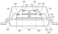
- FIG. 1 a shows a top view of one exemplary embodiment of a semiconductor chip package structure 500 of the invention.
- FIG. 1 b is a cross section taken along line A-A′ of FIG. 1 a showing one exemplary embodiment of a semiconductor chip package 500 of the invention.
- the semiconductor chip package structure 500 may comprise a lead frame based package of multi-chip integration, such as, a quad flat package (QFP). As shown in FIGS.
- the semiconductor chip package structure 500 comprises a lead frame 224 having a chip carrier 226 and a plurality of discrete leads 228 and 229 , wherein the leads 228 may serve as power leads 228 providing input/output electrical power connections.
- a first chip 200 is mounted on the chip carrier 226 by an adhesive material 212 , for example, silver paste or epoxy resin.
- the first chip 200 may comprise a multi-power chip 200 .
- the first chip 200 may be a chip 200 having level shifter circuits. Generally, an operating power provided to a chip is fixed. The first chip 200 having level shifter circuits may transfer operating power thereof to provide power to other chips or devices operating with different operating powers.
- the first chip 200 is operated through a first power connection, having a central region 202 and a marginal region 204 .
- the first chip 200 may comprise a plurality of first power bonding pads 207 , a plurality of second power bonding pads 206 and a plurality of bonding pads 208 , which are disposed in a marginal region 204 on the top of the first chip 200 .
- the first power bonding pads 207 , the second power bonding pads 206 and the bonding pads 208 may be arranged in a circular array adjacent to edges 203 of the first chip 200 .
- the first power bonding pads 207 and the second power bonding pads 206 may serve as input/output electrical power connections of the first chip 200
- the bonding pads 208 may serve as input/output electrical signal or ground connections of the first chip 200
- the first chip 200 may comprise a first power ring 270 and a second power ring 280 disposed in the first chip 200 . As shown in FIG. 1 a, the first power ring 270 and the second power ring 280 are parallel to each other and isolated from each other.
- the first power ring 270 and the second power ring 280 are in a position located directly under all the first power bonding pads 207 , the second power bonding pads 206 and the bonding pads 208 , substantially parallel to an arranged direction of the circular array formed by the bonding pads.
- the first power ring 270 and the second power ring 280 are in a position located in the marginal region 204 , but not directly under all the first power bonding pads 207 , the second power bonding pads 206 and the bonding pads 208 .
- the first power ring 270 are electrically connected to each of the first power bonding pads 207
- the second power rings are respectively electrically connected to each of the second power bonding pads 206 .
- first chip 200 may comprise ground paths or signal paths (not shown).
- a plurality of first bonding wires 222 are electrically connected to the leads 228 and the first power bonding pads 207 , respectively.
- the first bonding wire 222 a is electrically connected to the lead 228 a and the first power bonding pad 207 a.
- the first bonding wire 222 b is electrically connected to the lead 228 b and the first power bonding pad 207 b.
- the semiconductor chip package structure 500 further comprises a second chip 210 , wherein the first chip 300 may have an area larger than that of the second chip 210 .
- the second chip 210 may comprise a core logic chip 210 operating through a second power connection.
- the second chip 210 is mount on the central region 202 of the first chip 200 by an adhesive material 214 , for example, silver paste or epoxy resin.
- the second chip 210 may comprise a plurality of power bonding pads 216 and a plurality of bonding pads 217 , which are disposed on the top of the second chip 210 .
- the power bonding pads 216 and the bonding pads 217 may be arranged in a circular array adjacent to edges 211 of the second chip 210 .
- the power bonding pads 216 may serve as input/output electrical power connections of the second chip 210
- the bonding pads 217 may serve as input/output electrical signal or ground connections of the second chip 210 .
- the power bonding pads 216 of the second chip 210 may be respectively electrically connected to the second power bonding pads 206 through the second bonding wires 220 .
- the first chip 200 may provide power to the second chip 210 through the second power ring 280 .
- the power bonding pad 216 a of the second chip 210 is electrically connected to the second power bonding pad 206 a through a second bonding wire 220 a.
- the power bonding pad 216 b of the second chip 210 is electrically connected to the second power bonding pad 206 b through a second bonding wire 220 b.
- the power bonding pad 216 c of the second chip 210 is electrically connected to the second power bonding pad 206 c through a second bonding wire 220 c.
- the power bonding pad 216 d of the second chip 210 is electrically connected to the second power bonding pad 206 d through a second bonding wire 220 d.
- the drawings illustrate input/output electrical power connections of the first and second chips 200 and 210 for convenience only and is not limiting. The input/output electrical signal or ground connections of the first and second chips 200 and 210 are not illustrate herein.
- the semiconductor chip package structure 500 may further comprise a covering material 230 encapsulating the first chip 200 , the second chip 210 , the chip carrier 226 , inner portion of the leads 228 and 229 , the first bonding wires 222 and the second bonding wires 220 .
- the covering material 230 may comprise polymer materials, for example, epoxy resin.
- FIG. 2 a illustrates an enlarged view of a portion of FIG. 1 a showing the electrical connection relationship among the first power bonding pads 207 a and 207 b, the second power bonding pads 206 b to 206 d, the first power ring 270 and the second power ring 280 of one exemplary embodiment of a semiconductor chip package structure 500 of the invention.
- FIG. 2 b is a cross section taken along line B-B′ of FIG. 2 a showing the electrical connection relationship between the first power ring 270 and the first power bonding pad 207 b of one exemplary embodiment of a semiconductor chip package structure 500 of the invention.
- FIG. 2 c is a cross section taken along line C-C′ of FIG.
- FIG. 2 a showing the electrical connection relationship between the second power ring 280 and the second power bonding pad 260 d of one exemplary embodiment of a semiconductor chip package 500 of the invention.
- the first bonding wires 222 and the second bonding wires 220 as shown in FIG. 1 a are not illustrated herein for convenience only and is not limiting.
- the first and second power ring 270 and 280 are in a position directly under the first bonding pads 207 a and 207 b, the second power bonding pads 206 b to 206 d and the bonding pad 208 .
- the first and second power ring 270 and 280 are substantially parallel to an arranged direction of the first bonding pads 207 a and 207 b, the second power bonding pads 206 b to 206 d and the bonding pad 208 .
- a plurality of first power connections via plugs 242 are disposed in the first chip 200 , wherein the first power bonding pads 207 a and 207 b are respectively electrically connected to the first power ring 270 through the first power connections via plugs 242 .
- a plurality of second power connections via plugs 244 are disposed in the first chip 200 , wherein the second power bonding pads 206 b to 206 d are respectively electrically connected to the second power ring 280 through the second power connections via plugs 244 .
- the first power ring 270 and the second power ring 280 are disposed on a wafer 250 .
- the first power ring 270 or the second power ring 280 may be electrically connected to a semiconductor device 254 disposed on the wafer 250 .
- the first power ring 270 and the second power ring 280 are disposed in an interconnect structure 252 comprising dielectric layers 252 a to 252 d.
- the first power ring 270 and the second power ring 280 may be disposed in the same dielectric layer, for example, the dielectric layer 252 b.
- the first power ring 270 and the second power ring 280 may be disposed in dielectric layers with different levels (not shown), isolated from each other.
- the first power ring 270 is electrically connected to the first power bonding pad 207 b in the dielectric layer 252 d through the first power connections via plug 242 .
- the second power ring 280 is respectively electrically connected to the second power bonding pad 206 d in the dielectric layer 252 d through the second power connections via plug 244 .
- the electrical connection between the first power ring 270 and the corresponding first power bonding pads 207 or the second power ring 280 and the corresponding second power bonding pads 206 may allow the first power bonding pads 207 and the second power bonding pads 206 to have arbitrary arrangements, which allow for more flexible designs. As shown in FIG. 2 a, opposite sides of one of the first power bonding pads 207 along an arranged direction of the circular array, for example, the first power bonding pad 207 a, may be adjacent to the second power bonding pads 206 b and 26 c, respectively.
- opposite sides of one of the second power bonding pads 206 may be adjacent to the first power bonding pads 207 a and 207 b, respectively.
- the one of the first power bonding pads 207 and one of the second power bonding pads 206 may be disposed alternatively in relation to one another.
- any two of the first power bonding pads 207 may be spaced apart by an arbitrary number of the second power bonding pads 206 .
- any two of the second power bonding pads 206 may be spaced apart by an arbitrary number of the first power bonding pads 207 .
- number of the power rings with different operating powers and the respective corresponding power bonding pads is according to design, but not limited to the disclosure herein.
- the multi-power chip 200 a plurality of the parallel power rings with different operating powers may be respectively electrically connected to the power bonding pads with different operating powers through different power connections via plugs to input/output different operating powers, thereby providing power to other chips or devices operating with operating powers different from that of the first chip 200 .
- the first chip 200 may provide the operating power of the second chip 210 operated through a second power connection through the second power ring 280 . Therefore, layout area of the power rings can be reduced. The number of input/output electrical connections of the first chip 200 can also be reduced.
- One exemplary embodiment of the first chip 200 and the second chip 210 may be packaged by a lead frame based semiconductor package structure with lower cost.
- the electrical connection relationship between the second power ring and the second power bonding pad of one exemplary embodiment of a semiconductor chip package of the invention may allow the power bonding pads with different operating powers to have arbitrary arrangements, which allow for more flexible designs, to form the semiconductor chip package structure 500 by the lead frame based semiconductor chip package. Therefore, the semiconductor chip package structure 500 can be a multi-chip semiconductor chip package structure without using a costly ball grid array (BGA) semiconductor chip package structure.
- BGA ball grid array
Landscapes
- Wire Bonding (AREA)
- Semiconductor Integrated Circuits (AREA)
Abstract
Description
Claims (12)
Applications Claiming Priority (3)
| Application Number | Priority Date | Filing Date | Title |
|---|---|---|---|
| TW97208277 | 2008-05-13 | ||
| TW097208277U TWM343241U (en) | 2008-05-13 | 2008-05-13 | Semiconductor chip package structure |
| TW97208277U | 2008-05-13 |
Publications (2)
| Publication Number | Publication Date |
|---|---|
| US20090283918A1 US20090283918A1 (en) | 2009-11-19 |
| US7737541B2 true US7737541B2 (en) | 2010-06-15 |
Family
ID=41315408
Family Applications (1)
| Application Number | Title | Priority Date | Filing Date |
|---|---|---|---|
| US12/264,983 Active 2029-02-18 US7737541B2 (en) | 2008-05-13 | 2008-11-05 | Semiconductor chip package structure |
Country Status (2)
| Country | Link |
|---|---|
| US (1) | US7737541B2 (en) |
| TW (1) | TWM343241U (en) |
Cited By (1)
| Publication number | Priority date | Publication date | Assignee | Title |
|---|---|---|---|---|
| US20100007014A1 (en) * | 2008-07-11 | 2010-01-14 | Kabushiki Kaisha Toshiba | Semiconductor device |
Families Citing this family (5)
| Publication number | Priority date | Publication date | Assignee | Title |
|---|---|---|---|---|
| JP2013214611A (en) * | 2012-04-02 | 2013-10-17 | Elpida Memory Inc | Semiconductor device |
| US9136236B2 (en) | 2012-09-28 | 2015-09-15 | Intel Corporation | Localized high density substrate routing |
| US9190380B2 (en) | 2012-12-06 | 2015-11-17 | Intel Corporation | High density substrate routing in BBUL package |
| US9159690B2 (en) | 2013-09-25 | 2015-10-13 | Intel Corporation | Tall solders for through-mold interconnect |
| TWI550822B (en) * | 2014-03-03 | 2016-09-21 | 英特爾股份有限公司 | Device and package with localized high-density substrate winding and manufacturing method thereof |
Citations (1)
| Publication number | Priority date | Publication date | Assignee | Title |
|---|---|---|---|---|
| US20080237645A1 (en) * | 2007-03-27 | 2008-10-02 | Kabushiki Kaisha Toshiba | Semiconductor device |
-
2008
- 2008-05-13 TW TW097208277U patent/TWM343241U/en not_active IP Right Cessation
- 2008-11-05 US US12/264,983 patent/US7737541B2/en active Active
Patent Citations (1)
| Publication number | Priority date | Publication date | Assignee | Title |
|---|---|---|---|---|
| US20080237645A1 (en) * | 2007-03-27 | 2008-10-02 | Kabushiki Kaisha Toshiba | Semiconductor device |
Cited By (1)
| Publication number | Priority date | Publication date | Assignee | Title |
|---|---|---|---|---|
| US20100007014A1 (en) * | 2008-07-11 | 2010-01-14 | Kabushiki Kaisha Toshiba | Semiconductor device |
Also Published As
| Publication number | Publication date |
|---|---|
| US20090283918A1 (en) | 2009-11-19 |
| TWM343241U (en) | 2008-10-21 |
Similar Documents
| Publication | Publication Date | Title |
|---|---|---|
| US7834436B2 (en) | Semiconductor chip package | |
| US8860201B1 (en) | Stacked integrated circuit package using a window substrate | |
| KR100843214B1 (en) | Planar multi-semiconductor chip package in which memory chip and processor chip are connected through through electrode | |
| US8030748B2 (en) | Microelectronic device packages, stacked microelectronic device packages, and methods for manufacturing microelectronic devices | |
| US8288848B2 (en) | Semiconductor chip package including a lead frame | |
| US20180211943A1 (en) | Package substrate comprising side pads on edge, chip stack, semiconductor package, and memory module comprising same | |
| US12237302B2 (en) | Semiconductor package | |
| US20200279842A1 (en) | Double side mounted large mcm package with memory channel length reduction | |
| US7737541B2 (en) | Semiconductor chip package structure | |
| US20090302483A1 (en) | Stacked die package | |
| JP5350550B2 (en) | Powered and grounded package via via | |
| US20070257348A1 (en) | Multiple chip package module and method of fabricating the same | |
| KR102719915B1 (en) | Semiconductor package including stacked semiconductor chips | |
| US20080237645A1 (en) | Semiconductor device | |
| US6897555B1 (en) | Integrated circuit package and method for a PBGA package having a multiplicity of staggered power ring segments for power connection to integrated circuit die | |
| US20090294977A1 (en) | Semiconductor die and bond pad arrangement method thereof | |
| US8283765B2 (en) | Semiconductor chip and stacked semiconductor package having the same | |
| KR20200143885A (en) | Stack package including supporting substrate | |
| US20070007663A1 (en) | Semiconductor package having dual interconnection form and manufacturing method thereof | |
| CN101199052A (en) | Packaging logic and memory integrated circuits | |
| US20240387460A1 (en) | Semiconductor package and method of manufacturing the semiconductor package | |
| CN101599480B (en) | Semiconductor chip encapsulating structure | |
| US6509635B1 (en) | Integrated circuit package having offset die | |
| US7193314B2 (en) | Semiconductor devices and substrates used in thereof | |
| KR20080061604A (en) | Multichip Package |
Legal Events
| Date | Code | Title | Description |
|---|---|---|---|
| AS | Assignment |
Owner name: SILICON MOTION, INC., TAIWAN Free format text: ASSIGNMENT OF ASSIGNORS INTEREST;ASSIGNOR:CHYAN, YU-WEI;REEL/FRAME:021787/0693 Effective date: 20081022 Owner name: SILICON MOTION, INC.,TAIWAN Free format text: ASSIGNMENT OF ASSIGNORS INTEREST;ASSIGNOR:CHYAN, YU-WEI;REEL/FRAME:021787/0693 Effective date: 20081022 |
|
| STCF | Information on status: patent grant |
Free format text: PATENTED CASE |
|
| FPAY | Fee payment |
Year of fee payment: 4 |
|
| FPAY | Fee payment |
Year of fee payment: 8 |
|
| FEPP | Fee payment procedure |
Free format text: ENTITY STATUS SET TO UNDISCOUNTED (ORIGINAL EVENT CODE: BIG.); ENTITY STATUS OF PATENT OWNER: LARGE ENTITY |
|
| MAFP | Maintenance fee payment |
Free format text: PAYMENT OF MAINTENANCE FEE UNDER 1.28(C) (ORIGINAL EVENT CODE: M1559); ENTITY STATUS OF PATENT OWNER: LARGE ENTITY |
|
| MAFP | Maintenance fee payment |
Free format text: PAYMENT OF MAINTENANCE FEE, 12TH YEAR, LARGE ENTITY (ORIGINAL EVENT CODE: M1553); ENTITY STATUS OF PATENT OWNER: LARGE ENTITY Year of fee payment: 12 |
|
| FEPP | Fee payment procedure |
Free format text: PETITION RELATED TO MAINTENANCE FEES GRANTED (ORIGINAL EVENT CODE: PTGR); ENTITY STATUS OF PATENT OWNER: LARGE ENTITY |