US7732978B2 - Piezoelectric element driving circuit and pump device - Google Patents
Piezoelectric element driving circuit and pump device Download PDFInfo
- Publication number
- US7732978B2 US7732978B2 US12/220,007 US22000708A US7732978B2 US 7732978 B2 US7732978 B2 US 7732978B2 US 22000708 A US22000708 A US 22000708A US 7732978 B2 US7732978 B2 US 7732978B2
- Authority
- US
- United States
- Prior art keywords
- driving
- circuit
- piezoelectric element
- voltage
- transformer
- Prior art date
- Legal status (The legal status is an assumption and is not a legal conclusion. Google has not performed a legal analysis and makes no representation as to the accuracy of the status listed.)
- Expired - Fee Related, expires
Links
Images


Classifications
-
- H—ELECTRICITY
- H10—SEMICONDUCTOR DEVICES; ELECTRIC SOLID-STATE DEVICES NOT OTHERWISE PROVIDED FOR
- H10N—ELECTRIC SOLID-STATE DEVICES NOT OTHERWISE PROVIDED FOR
- H10N30/00—Piezoelectric or electrostrictive devices
- H10N30/80—Constructional details
- H10N30/802—Circuitry or processes for operating piezoelectric or electrostrictive devices not otherwise provided for, e.g. drive circuits
Definitions
- the present invention contains subject matter related to Japanese Patent Application JP 2007-211912 filed in the Japan Patent Office on Aug. 15, 2007, the entire contents of which being incorporated herein by reference.
- the present invention relates to a highly efficient piezoelectric element driving circuit that can vary driving voltage and consumes low power and a pump device that transfers a fluid by the vibration of a piezoelectric element.
- a piezoelectric element makes a mechanical movement according to an applied voltage because a piezoelectric material is bent when an electric field is applied to the piezoelectric material. Utilizing this characteristic of converting electric energy into kinetic energy, piezoelectric elements are widely applied to actuators, motors, and the like.
- a driving circuit in which a resonant element such as a capacitor or the like forming a resonant circuit is connected to a primary side coil of a transformer, and primary side driving frequency is made variable is known as a driving circuit for a piezoelectric element of an oscillatory wave motor (see Japanese Patent Publication No. Hei 5-16277 (hereinafter referred to as Patent Document 1), for example).
- a new actuator using a mode of coupled-vibration with a peripheral structure rather than a discrete piezoelectric element has recently been proposed.
- a piezoelectric element and the peripheral structure vibrate in a mechanically coupled manner.
- behavior in the coupled-vibration mode at this time is complex.
- the Q-value of mechanical resonance frequency often becomes high.
- a method of combining a variable output voltage power supply with a driving circuit is conceivable for a purpose of controlling the mechanical output of the actuator at a fixed driving frequency. This method is also described in Patent Document 1.
- a variable output voltage power supply circuit on a relatively large circuit scale is necessary separately from a driving circuit.
- a driving circuit in which a reactance element such as an inductor or the like forming a parallel resonant circuit together with a load (a piezoelectric element or a piezoelectric motor) on a secondary side of a transformer is provided, and driving frequency is stabilized by optimizing a constant of the reactance element so as to make the resonance frequency of the parallel resonant circuit coincide with the driving frequency (see Japanese Patent No. 2976489 (hereinafter referred to as Patent Document 2), for example).
- Patent Document 2 Japanese Patent No. 2976489
- Patent Document 2 discloses a switch circuit that applies a power supply voltage to a midpoint of a primary winding of the transformer and that alternately grounds both ends of the primary winding in order to realize a zero cross waveform of the secondary side voltage.
- the driving circuit having such a configuration and operation can remove a ripple and reduce a loss, and also makes it possible to set the driving duty ratio of a switching element connected to the primary side of the transformer at a simple 50%.
- driving voltage for the piezoelectric element may not be varied, and input power for the piezoelectric element may not be varied, unless a variable voltage power supply is provided outside the circuit.
- a fluid pump device using a piezoelectric element may need to control an amount of fluid being transferred. At this time, it is necessary to change input power for the piezoelectric element.
- the application of the actuator using the piezoelectric element is expected to be widened to not only uses in conventional stationary devices but also uses in portable devices. At this time, power saving and miniaturization of the driving circuit also become important factors.
- a piezoelectric element driving circuit includes a transformer, a switch circuit, a reactance element, a pulse generating circuit, and a duty ratio controlling circuit.
- the transformer has a turns ratio at which a rate of a number of turns of a secondary winding on a load side is high with respect to a number of turns of a primary winding on a power supply side, exceeding a ratio of a power supply side voltage value to a specification voltage value on the load side.
- the switch circuit performs switching operation on power supply voltage at a driving frequency on a primary side of the transformer to apply a driving voltage to a piezoelectric element connected to a secondary side of the transformer.
- the transformer has a primary side winding circuit and a secondary side winding circuit.
- the transformer transforms a voltage input to the primary side winding circuit as a result of the switching operation of the switch circuit, and outputs the transformed voltage to the secondary side winding circuit.
- an inductance component when the transformer is viewed from the side of the secondary side winding circuit forms a resonant circuit at a time of resonant operation.
- the reactance element is connected in parallel with the piezoelectric element on the secondary side of the transformer.
- the reactance element forms the resonant circuit that performs parallel resonance at the driving frequency with a capacitance component in an equivalent circuit of the piezoelectric element and the inductance component of the transformer.
- the pulse generating circuit generates and outputs a driving pulse at a frequency equal to resonance frequency, for example.
- the duty ratio controlling circuit is supplied with the driving pulse from the pulse generating circuit.
- the duty ratio controlling circuit limits the duty ratio of the driving pulse according to, for example, a voltage controlling signal input to the duty ratio controlling circuit such that the value of the driving voltage falls within a range equal to or lower than the specification voltage value on the load side.
- the duty ratio controlling circuit outputs the driving pulse whose duty ratio is limited to the switch circuit.
- the switch circuit drives the power supply voltage at the driving frequency on the primary side of the transformer. Therefore, the driving voltage having a magnitude corresponding to the turns ratio of the transformer is applied to the piezoelectric element connected to the secondary side of the transformer.
- the resonant circuit formed by the reactance element connected in parallel with the piezoelectric element on the secondary side of the transformer, the capacitance component of the piezoelectric element, and the inductance component of the transformer performs parallel resonance at the driving frequency.
- the switch circuit performs switching operation to change potential on the secondary side of the transformer to a predetermined potential.
- the driving voltage for the piezoelectric element is originally increased according to the turns ratio of the transformer.
- the turns ratio is set such that the rate of the number of turns of the secondary winding is higher, exceeding the ratio between the power supply side voltage value and the specification voltage value on the load side.
- the power consumed by the switch circuit is a time average of power consumed during times that the driving pulse is on. Therefore, when the duty ratio of the driving pulse becomes relatively low, the power consumed by the switch circuit is correspondingly reduced.
- a pump device includes: a pump having a pump chamber one side of which is sealed by one of a piezoelectric material of a piezoelectric element and a vibrating member vibrating together with the piezoelectric material, the pump discharging, from a discharge opening, a fluid sucked in from a fluid suction opening of the pump chamber; and a driving circuit for vibrating and driving the piezoelectric element of the pump.
- the driving circuit includes a transformer, a switch circuit, a reactance element, a pulse generating circuit, and a duty ratio controlling circuit.
- the pump device of such a constitution can be used for air cooling or water cooling, for example.
- the driving circuit applies an alternating voltage to the piezoelectric material of the piezoelectric element sealing one side of the pump chamber, the piezoelectric material vibrates, increasing and decreasing pressure within the pump chamber.
- the piezoelectric material operates so as to expand the space of the pump chamber, the pressure within the pump chamber is decreased, and a fluid is taken in from the fluid suction opening.
- the piezoelectric material operates so as to contract the space of the pump chamber, a pressure is applied to the fluid within the pump chamber, so that the fluid within the pump is pushed out and swiftly discharged from the discharge opening to the outside.
- the driving circuit drives the piezoelectric element such that the piezoelectric material performs the operation of expanding the space of the pump chamber and the operation of contracting the space of the pump chamber at a predetermined frequency.
- piezoelectric element driving voltage may not necessarily be so high as to require the switch circuit to be operated in each cycle of the resonance frequency.
- a stop controlling circuit is desirably newly provided in such a manner as to be included in the driving circuit. That is, the present invention preferably has the stop controlling circuit for periodically stopping the switching operation of the switch circuit for an arbitrary period.
- the stop controlling circuit can intermittently stop the switching operation of the switch circuit in cycles of m (an arbitrary natural number) times the driving frequency, for example. Thus, energy replenishment is not performed when the switching operation of the switch circuit is stopped periodically.
- the stop controlling circuit is preferably configured to control the input power for the piezoelectric element by changing the frequency (cycle) of the stopped operation during which energy replenishment is not performed.
- the present invention it is possible to perform efficient driving with a simple constitution and at a desired frequency, and to provide a piezoelectric element driving circuit that can change input power input to a piezoelectric element and reduce power consumption and a pump device using the driving circuit.
- FIG. 1A and FIG. 1B are circuit block diagrams showing configurations of driving circuits according to a first embodiment, FIG. 1A being a diagram illustrating a case where a reactance element is connected and disposed on the secondary side of an electromagnetic coupling transformer 2 , and FIG. 1B being a diagram illustrating a case where a reactance element is connected and disposed on the primary side of an electromagnetic coupling transformer 2 ;
- FIG. 2 is a concrete circuit diagram of a unipolar type driving circuit according to the first embodiment
- FIGS. 3A to 3G are diagrams of operating waveforms of the circuit shown in FIG. 2 ;
- FIGS. 4A to 4C are diagrams of operating waveforms when a driving duty ratio is relatively low
- FIGS. 5A to 5C are diagrams of operating waveforms when the driving duty ratio is relatively high
- FIG. 6 is a concrete circuit diagram of a bipolar type driving circuit according to the first embodiment
- FIGS. 7A to 7F are diagrams of operating waveforms of the circuit shown in FIG. 6 ;
- FIG. 8A is a graph showing changes in driving voltage value when the driving duty ratio is varied by changing a voltage controlling signal
- FIG. 8B is a graph showing changes in average driving current when the driving duty ratio is varied similarly;
- FIG. 9A and FIG. 9B are circuit block diagrams showing configurations of driving circuits according to a second embodiment, FIG. 9A being a diagram illustrating a case where a reactance element is connected and disposed on the secondary side of an electromagnetic coupling transformer 2 , and FIG. 9B being a diagram illustrating a case where a reactance element is connected and disposed on the primary side of an electromagnetic coupling transformer 2 ;
- FIG. 10 is a concrete circuit diagram of a unipolar type driving circuit according to the second embodiment.
- FIG. 11 is a diagram showing an oscillation waveform at a time of stop control in the circuit of FIG. 9A ;
- FIG. 12 is an assembly diagram of an air pump device used as an air cooling device according to a third embodiment.
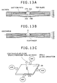
- FIGS. 13A to 13C are diagrams showing air paths of an air pump device, FIG. 13A being a schematic sectional view of the air pump device, showing an air path at a time of a suction, FIG. 13B being a schematic sectional view of the air pump device, showing an air path at a time of a discharge, and FIG. 13C being a diagram showing an air flow when the air pump device is viewed at an angle.
- the present embodiment relates to an embodiment of a “piezoelectric element driving circuit” according to the present invention.
- FIG. 1A and FIG. 1B are circuit block diagrams of piezoelectric element driving circuits.
- the driving circuits 1 A and 1 B illustrated in FIG. 1A and FIG. 1B each include an electromagnetic coupling transformer 2 , a switch circuit 3 , a reactance element 4 , a pulse generating circuit 5 , and a duty ratio controlling circuit 6 .
- the driving circuits 1 A and 1 B shown in FIG. 1A and FIG. 1B each have the electromagnetic coupling transformer 2 .
- the electromagnetic coupling transformer 2 includes a primary side winding circuit, a secondary side winding circuit, and a magnetic material having a relative permeability of one or more between the two winding circuits.
- the two winding circuits are electromagnetically coupled to each other by the magnetic material.
- the electromagnetic coupling transformer 2 has a turns ratio exceeding a ratio of a power supply side voltage value to a specification voltage value on a load side. More specifically, the electromagnetic coupling transformer 2 according to the present embodiment has a turns ratio such that the rate of the number of turns of a secondary winding W 2 on the load side is high with respect to the rate of the number of turns of a primary winding W 1 on a power supply side as compared with a normal ratio of the number of turns of the primary winding W 1 to the number of turns of the secondary winding W 2 , the normal ratio being defined by the above-described ratio of the power supply side voltage value to the specification voltage value on the load side.
- FIG. 1A is a diagram showing the reactance element 4 being connected in parallel with the secondary side winding circuit of the electromagnetic coupling transformer 2 .
- FIG. 1B is a diagram showing the reactance element 4 being connected in parallel with the primary side winding circuit of the electromagnetic coupling transformer 2 .
- Whether the winding circuit side to which the reactance element 4 is connected is the primary side or the secondary side of the electromagnetic coupling transformer 2 may be determined according to the withstand voltage specification or the reactance value of the reactance element 4 .
- the switch circuit 3 is connected to the primary winding W 1 of the electromagnetic coupling transformer 2 , and a piezoelectric element PZ is connected to the secondary winding W 2 of the electromagnetic coupling transformer 2 .
- the pulse generating circuit 5 is connected to the duty ratio controlling circuit 6 , and the duty ratio controlling circuit 6 is connected to the switch circuit 3 so that a pulse signal generated by the pulse generating circuit 5 can be input to the switch circuit 3 after the duty ratio of the pulse signal is controlled by the duty ratio controlling circuit 6 .
- a power supply voltage Vdd for driving the driving circuits 1 A and 1 B and a reference voltage (for example a ground voltage GND) are supplied from an external power supply circuit (POWER) 10 .
- a voltage controlling signal Vcont for the duty ratio controlling circuit 6 is also supplied externally.
- the switch circuit 3 controlled by the pulse signal operates so as to repeatedly set the primary winding W 1 to an on state in which a current is passed through the primary winding W 1 and an off state in which the current is not passed through the primary winding W 1 at a predetermined frequency specified by the input pulse signal.
- the on state corresponds to the high level of the pulse
- the off state corresponds to the low level of the pulse.
- the frequency (period T) of primary side current driving of the electromagnetic coupling transformer 2 is defined as current driving frequency.
- the current driving frequency is desirably set to coincide with the resonance frequency of a resonant circuit formed by the secondary side winding circuit. While operation is possible even when the current driving frequency does not perfectly coincide with the resonance frequency, it is desirable that the current driving frequency coincide with the resonance frequency in order to make the waveform of voltage applied to the piezoelectric element a sinusoidal wave and perform efficient driving, as will be described later.
- One of features of the driving circuits 1 A and 1 B is the intermittent primary side driving of the electromagnetic coupling transformer 2 which driving is performed by repeating the on state and the off state described above.
- the current driving is performed by sending current intermittently with a current stop state in between. Due to such current driving, power consumed by the switch circuit 3 on the primary side is relatively low because the power consumed by the switch circuit 3 is a time average of power consumed by pulse current of short duration.
- Another feature is that the on time of the driving pulse can be shortened by setting the turns ratio of the electromagnetic coupling transformer 2 higher than the normal ratio. Details of this point will be described later.
- an alternating voltage is applied to the piezoelectric element PZ due to a resonance phenomenon of the resonant circuit on the secondary side.
- the alternating voltage gradually attenuates. This attenuation is caused by a loss of energy due to a copper loss of the resonant circuit (winding circuit) or the like.
- energy replenishment by a next pulse current from the primary side is performed for a short time before the positive peak value and the negative peak value of the alternating voltage supplied to the piezoelectric element PZ on the secondary side of the electromagnetic coupling transformer 2 each attenuate, and this is repeated cyclically.
- energy replenishment may be performed cyclically for a short time after the alternating voltage supplied to the piezoelectric element PZ attenuates to a certain degree.
- the resonant circuit there is no electric discharge path from the resonant circuit to the outside (for example, the GND line), and electric discharge to the outside is not substantially performed.
- a loss of energy due to a copper loss of the resonant circuit (winding circuit) or the like is compensated for by intermittent current driving from the primary side. All of the energy loss is compensated for from the primary side to an absolute minimum degree.
- the magnitude of an equivalent capacitance value of the piezoelectric element PZ is determined according to a use of the piezoelectric element PZ. It can be difficult to make the current driving frequency coincide with or substantially equal the resonance frequency of the resonant circuit by merely changing the frequency (current driving frequency) of the pulse signal generated by the pulse generating circuit 5 .
- the reactance element 4 is added to the resonant circuit to make the current driving frequency coincide with or substantially equal the resonance frequency of each resonant circuit.
- the reactance element 4 forms the resonant circuit that performs parallel resonance at the (current) driving frequency with a capacitance component in an equivalent circuit of the piezoelectric element PZ and an inductance component of the electromagnetic coupling transformer 2 .
- the reactance element 4 can be added to the resonant circuit by connecting a capacitor in parallel with the piezoelectric element PZ or connecting an inductor in parallel with or in series with the piezoelectric element PZ.
- FIG. 2 is a more detailed diagram than FIG. 1A , showing a concrete example of the circuit according to the present embodiment.
- FIGS. 3A to 3G are diagrams of operating waveforms of the circuit shown in FIG. 2 .
- the pulse generating circuit 5 shown in FIG. 2 includes two current sources 11 and 12 , an amplifier AMP, a comparator CMP 1 , a switch SW 1 , a capacitor C 1 , and a resistance R 1 .
- the current source I 1 and the capacitor C 1 are connected in series with each other between a terminal for supplying the power supply voltage Vdd of the power supply circuit 10 and a terminal for supplying the ground voltage GND of the power supply circuit 10 .
- the current source I 2 and the resistance R 1 are connected in series with each other between the terminal for supplying the power supply voltage Vdd and the terminal for supplying the ground voltage GND.
- the non-inverting input “+” of the comparator CMP 1 is connected to a point of connection between the current source I 1 and the capacitor C 1 , so that a voltage V 1 at the point of connection can be input to the non-inverting input of the comparator CMP 1 .
- the inverting input “ ⁇ ” of the comparator CMP 1 is connected to a point of connection between the current source I 2 and the resistance R 1 , so that a voltage V 2 at the point of connection can be input to the inverting input of the comparator CMP 1 .
- the switch SW 1 is connected between the non-inverting input “+” of the comparator CMP 1 and the terminal for supplying the ground voltage GND so as to be able to discharge a voltage retained by the capacitor C 1 .
- the switch SW 1 is controlled according to the output of the comparator CMP 1 .
- the voltage V 1 can be output from the pulse generating circuit 5 after being amplified by the amplifier AMP.
- the amplifier AMP has a high input impedance and a low output impedance.
- the amplifier AMP serves a function of impedance conversion as an amplifier referred to generally as a buffer amplifier.
- the duty ratio controlling circuit 6 is formed by one comparator CMP 2 .
- the comparator CMP 2 has an inverting input “ ⁇ ” connected to the output of the amplifier AMP, and has a non-inverting input “+” connected to the terminal for supplying the voltage controlling signal Vcont.
- the voltage controlling signal Vcont is generated by an external variable voltage source 11 , and then supplied to the duty ratio controlling circuit 6 .
- the switch circuit 3 includes one diode D 1 and an NMOS transistor Q 1 .
- the primary winding W 1 of the electromagnetic coupling transformer 2 is connected between the terminal for supplying the power supply voltage Vdd and the anode of the diode D 1 .
- the NMOS transistor Q 1 is connected between the cathode of the diode D 1 and the terminal for supplying the ground voltage GND.
- the gate of the NMOS transistor Q 1 is connected to the output of the comparator CMP 2 .
- the diode D 1 is a reverse current preventing diode for preventing a flow of driving current caused by the body diode of the NMOS transistor Q 1 when the gate voltage (signal Vg) of the NMOS transistor Q 1 is at a low level.
- the diode D 1 can be omitted when the effect of the body diode is negligible.
- FIG. 3A shows the waveforms of the voltages V 1 and V 2 , which are voltages input to the comparator CMP 1 in FIG. 2 .
- FIG. 3B shows the waveform of gate voltage of the switch SW 1 .
- a current flowing through the resistance R 1 in FIG. 2 is generated by the current source I 2 , a fixed stable potential difference (the voltage V 2 ) occurs in the resistance R 1 , as shown in FIG. 3A .
- a potential difference (the voltage V 1 ) occurs across the capacitor C 1 which potential difference increases in proportion to an elapsed time during which a current is applied across the capacitor C 1 .
- the voltage V 1 increases monotonically while the capacitor C 1 is charged.
- the comparator CMP 1 compares the voltage V 2 across the resistance R 1 with the voltage (voltage V 1 ) retained by the capacitor C 1 .
- the comparator CMP 1 turns on the switch SW 1 , which is normally in an opened state ( FIG. 3B ). Then, a charge stored in the capacitor C 1 is discharged via the switch SW 1 .
- the voltage (voltage V 1 ) retained by the capacitor C 1 therefore becomes zero ( FIG. 3A ).
- the comparator CMP 1 turns off the switch SW 1 , so that the voltage (voltage V 1 ) retained by the capacitor C 1 monotonically increases again.
- FIG. 3C shows the waveforms of voltages input to the comparator CMP 2 .
- FIG. 3D shows the waveform of the output voltage of the comparator CMP 2 , that is, the signal Vg applied to the gate of the NMOS transistor Q 1 .
- a sawtooth-shaped pulse wave Vramp is output from the pulse generating circuit 5 in FIG. 2 , as shown in FIG. 3C .
- the oscillation frequency of the pulse wave Vramp is made to coincide substantially with the resonance frequency on the secondary side of the electromagnetic coupling transformer 2 by setting each of the value of the capacitor C 1 , the respective current values of the current sources 11 and 12 , and the value of the resistance R 1 to an appropriate value.
- the voltage controlling signal Vcont supplied from the outside of the driving circuit 1 A is an arbitrary DC signal, and is a signal intended to control a driving signal Vout ( FIG. 2 and FIG. 3G ) supplied to the piezoelectric element PZ.
- the comparator CMP 2 as the duty ratio controlling circuit 6 compares the voltage values of the pulse wave Vramp and the voltage controlling signal Vcont with each other ( FIG. 3C ).
- the comparator CMP 2 outputs the signal Vg for controlling the on state and the off state of the switch circuit 3 according to a result of the comparison, as shown in FIG. 3D .
- the switch circuit 3 assumes the on state in which the switch circuit 3 passes an output current.
- the switch circuit 3 assumes the off state in which the switch circuit 3 does not pass an output current.
- the primary side current Id of the electromagnetic coupling transformer 2 is also the output current of the switch circuit 3 .
- the switch circuit 3 When the switch circuit 3 is in the on state for a short time, the primary side current Id rises linearly as shown in FIG. 3F after the switch (NMOS transistor Q 1 ) is set in the on state, due to a leakage inductance on the primary side of the electromagnetic coupling transformer 2 .
- a pseudo-sinusoidal wave whose peak value is limited according to the primary side current Id appears on the primary side of the electromagnetic coupling transformer 2 .
- a sinusoidal wave of a magnitude corresponding to the turns ratio of the electromagnetic coupling transformer 2 appears as driving signal Vout in the secondary winding W 2 of the electromagnetic coupling transformer 2 .
- T be a period of the signal Vg
- ton be a pulse duration
- a time during which the switch circuit 3 is in the on state is changed depending on the duty ratio (ton/T)
- the peak value of the primary side current Id is also changed depending on the duty ratio.
- the duty ratio of the signal Vg can be controlled by the magnitude of the voltage controlling signal Vcont.
- FIGS. 4A to 4C and FIGS. 5A to 5C show states in which the primary side current Id and the secondary side voltage, that is, the driving signal Vout for the piezoelectric element PZ are changed depending on the duty ratio of the signal Vg.
- FIG. 4A and FIG. 5A each show the waveform of the signal Vg.
- FIG. 4B and FIG. 5B each show the waveform of the primary side current Id.
- FIG. 4C and FIG. 5C each show the waveform of the driving signal Vout.
- the signal Vg of FIG. 4A has a lower duty ratio than the signal Vg of FIG. 5A . This is because the voltage controlling signal Vcont is controlled to be relatively small in FIG. 3C .
- the low duty ratio of the signal Vg makes the peak value of the primary side current Id in FIG. 4B also relatively low. As a result, the amplitude of the driving signal Vout is also low depending on the peak value of the primary side current Id.
- the present embodiment enables the driving amplitude for the piezoelectric element PZ to be controlled to an appropriate value by changing the duty ratio of the pulse signal driving the switch circuit 3 .
- the resonance frequency fdrv when the piezoelectric element PZ is driven is set in the resonant circuit in a state in which the transistor (NMOS transistor Q 1 ) within the switch circuit 3 is off. This is to reduce power consumption of the driving circuit.
- the resonance frequency fdrv is expressed by the following Equation (1-1) or Equation (1-2) with the reactance component Xext connected in parallel with the capacitance component Cpz of the piezoelectric element, the secondary side leakage inductance component L 2 of the electromagnetic coupling transformer 2 , and the mutual inductance M of the electromagnetic coupling transformer 2 .
- Equation (1-1) expresses the resonance frequency fdrv when the reactance component Xext is a capacitive component.
- Equation (1-2) expresses the resonance frequency fdrv when the reactance component Xext is an inductive component.
- the NMOS transistor Q 1 in the on state is in a state of low impedance. Therefore, the primary side of the electromagnetic coupling transformer 2 is in a short-circuited state, as it were.
- the primary side leakage inductance L 1 of the primary side winding circuit and the mutual inductance M of the electromagnetic coupling transformer 2 are connected in parallel with each other.
- the primary side leakage inductance L 1 is a value of a few percent of the mutual inductance M, and thus the on-time mutual inductance M(on) is also a value of a few percent of the (off-time) mutual inductance M.
- the resonance frequency when the NMOS transistor Q 1 is in the on state is increased by about an order of magnitude as compared with the resonance frequency fdrv at the time of driving the piezoelectric element.
- the switch circuit 3 shows response faster than at the resonance frequency fdrv set with the NMOS transistor Q 1 in the off state, and driving current rises quickly.
- the on period of the NMOS transistor Q 1 may be from a time when the NMOS transistor Q 1 is set in the on state and the driving current (primary side current Id) starts to flow to a time when the driving current reaches a peak value after the slope of increase in primary side current Id gradually decreases. This is because when the driving current reaches the peak value, the amplitude of the voltage in the secondary side resonant circuit of the electromagnetic coupling transformer 2 also reaches a peak value.
- Retaining the output transistor in the on state even when the driving current has passed the peak value is meaningless in terms of controlling the resonance voltage on the secondary side of the electromagnetic coupling transformer 2 , and causes unnecessary consumption of driving power.
- the duty ratio controlling circuit 6 is supplied with a driving pulse from the pulse generating circuit 5 .
- the duty ratio controlling circuit 6 limits the duty ratio of the driving pulse according to the input voltage controlling signal Vcont such that the value of the driving voltage generated in the secondary winding W 2 of the electromagnetic coupling transformer 2 falls within a range equal to or lower than a specification voltage value on the load side.
- the “specification voltage value on the load side” refers to for example a maximum rated voltage of the piezoelectric element PZ or a recommended application voltage.
- the duty ratio controlling circuit 6 outputs the driving pulse whose duty ratio is limited to the switch circuit 3 .
- the driving voltage for the piezoelectric element PZ is intrinsically increased according to the turns ratio of the electromagnetic coupling transformer 2 .
- the turns ratio is set such that the rate of the number of turns of the secondary winding W 2 is higher, exceeding the ratio between the power supply side voltage value and the specification voltage value on the load side.
- the power consumed by the switch circuit 3 is a time average of power consumed during times that the driving pulse is on. Therefore, when the duty ratio of the driving pulse becomes relatively low, the power consumed by the switch circuit 3 is correspondingly reduced.
- the time of the on state of the NMOS transistor Q 1 is thus limited by controlling the duty ratio of the driving pulse by the duty ratio controlling circuit 6 , whereby input power for the piezoelectric element PZ can be controlled such that lower power consumption is achieved.
- FIG. 6 is another concrete circuit diagram relating to the first embodiment.
- FIGS. 7A to 7F are diagrams of operating waveforms of a circuit of FIG. 6 .
- a switch circuit 3 of the circuit illustrated in FIG. 6 is different from that of the circuit illustrated in FIG. 2 described above.
- a pulse generating circuit 5 is connected to the switch circuit 3 via a duty ratio controlling circuit 6 , and the duty ratio controlling circuit 6 controls the duty ratio of a driving pulse for the switch circuit 3 .
- an input A and an input B are used in FIG. 6 in place of the signal Vg in FIG. 2 .
- the input A and the input B are, for example, signals shifted in phase from each other by a half cycle and differentially operating transistors connected to the respective inputs.
- the duty ratio controlling circuit 6 not shown in the figure controls the duty ratio of each of the input A and the input B according to a voltage controlling signal Vcont input to the duty ratio controlling circuit 6 .
- the primary side of the electromagnetic coupling transformer 2 in the circuit of FIG. 2 already described has two states, that is, the on state in which the primary side current Id flows through the primary winding W 1 in one direction and the off state in which the primary side current Id does not flow through the primary winding W 1 .
- Such driving is generally referred to as unipolar driving.
- the primary side of a electromagnetic coupling transformer 2 in the circuit of FIG. 6 has three states, that is, an on state in which a primary side current Id flows through a primary winding W 1 in one direction (positive direction), an on state in which the primary side current Id flows through the primary winding W 1 in an opposite direction (negative direction), and an off state in which the primary side current Id does not flow through the primary winding W 1 .
- Such driving is generally referred to as bipolar driving.
- FIG. 6 illustrates a driving circuit that drives two piezoelectric elements PZ 1 and PZ 2 .
- the secondary winding W 2 of the electromagnetic coupling transformer 2 includes two second winding coils W 21 and W 22 .
- the piezoelectric element PZ 1 forms a resonant circuit together with an auxiliary capacitor Caxu. 1 and the second winding coil W 21 .
- the piezoelectric element PZ 2 forms another resonant circuit together with an auxiliary capacitor Caxu. 2 and the second winding coil W 22 .
- the values of the auxiliary capacitors Caxu. 1 and Caxu. 2 of the two resonant circuits are each determined such that the two resonant circuits have a same resonance frequency.
- the resonance frequency of the resonant circuit is determined by a combined capacitance of an equivalent capacitance component of the piezoelectric element PZ 1 and the auxiliary capacitor Caxu.
- the resonance frequency of the other resonant circuit is determined by a combined capacitance of an equivalent capacitance component of the piezoelectric element PZ 2 and the auxiliary capacitor Caxu. 2 and an inductance of the second winding coil W 22 .
- one electrode of the piezoelectric element PZ 1 and one electrode of the piezoelectric element PZ 2 are connected to each other on the side of a midpoint node N.
- the auxiliary capacitor Caxu. 1 is connected between the midpoint node N and another electrode of the piezoelectric element PZ 1 .
- the auxiliary capacitor Caxu. 2 is connected between the midpoint node N and another electrode of the piezoelectric element PZ 2 .
- This midpoint node N is connected to a ground voltage GND. This is to eliminate an effect of static electricity. Incidentally, the connection of the midpoint node N to the ground voltage GND does not affect operation because a path through the midpoint node N to the ground voltage GND does not form a discharge path at a time of high-frequency driving.
- the switch circuit 3 connected to the primary winding W 1 of the electromagnetic coupling transformer 2 is an H-bridge circuit of a four-transistor configuration as shown in FIG. 6 .
- the switch circuit 3 has two PMOS transistors P 1 and P 2 and two NMOS transistors N 1 and N 2 .
- the primary winding W 1 is connected between nodes ND 1 and ND 2 within the switch circuit 3 .
- the source of the transistor P 1 is connected to a terminal for supplying a power supply voltage Vdd.
- the drain of the transistor P 1 is connected to the node ND 1 .
- the gate of the transistor P 1 is connected to the node ND 2 .
- the source of the transistor P 2 is connected to the terminal for supplying the power supply voltage Vdd.
- the drain of the transistor P 2 is connected to the node ND 2 .
- the gate of the transistor P 2 is connected to the node ND 1 .
- the drain of the transistor N 1 is connected to the node ND 2 .
- the source of the transistor N 1 is connected to a terminal for supplying the ground voltage GND.
- the gate of the transistor N 1 is connected to a terminal for supplying the input A.
- the drain of the transistor N 2 is connected to the node ND 1 .
- the source of the transistor N 2 is connected to the terminal for supplying the ground voltage GND.
- the gate of the transistor N 2 is connected to a terminal for supplying the input B.
- the transistors N 1 and P 1 are turned on, so that a positive current I(+) flows through the transistor P 1 in the on state, the node ND 1 , the primary winding W 1 , the node ND 2 , and the transistor N 1 in the on state to the ground voltage GND (see FIG. 6 ).
- the transistors N 2 and P 2 are turned on, so that a negative current I( ⁇ ) flows through the transistor P 2 in the on state, the node ND 2 , the primary winding W 1 , the node ND 1 , and the transistor N 2 in the on state to the ground voltage GND (see FIG. 6 ).
- the period of “H” of the input A is defined by a pulse of a duration (indicated by ON(+)) shorter than a fixed half cycle T/2. This pulse is repeated in fixed cycles T.
- the period of “H” of the input B is defined by a short duration (indicated by ON( ⁇ )) different in phase from the pulse of the input A by 180 degrees and having the same cycle T.
- the durations (so-called pulse widths) of the two pulses may be different from each other. In this case, however, suppose that the durations of the two pulses are the same.
- the duration of the pulse of the input A will be referred to as a “positive current driving time” or an “ON(+) time”.
- the duration of the pulse of the input B will be referred to as a “negative current driving time” or an “ON( ⁇ ) time”.
- a fixed off state period during which no current flows through the primary winding W 1 exists between an ON(+) time and a next ON( ⁇ ) time and between the ON( ⁇ ) time and a next ON(+) time.
- the four transistors N 1 , N 2 , P 1 , and P 2 forming the switch circuit 3 shown in FIG. 6 are all off, and thus the switch circuit 3 is in a state of high impedance as viewed from both ends of the primary winding W 1 .
- a current at a level of an off leak of the transistors flows, and therefore power consumption is practically equal to zero.
- the magnitude (absolute value) of the positive current I(+) and the negative current I( ⁇ ) is represented by “
- the pulse being turned on the current starts to flow and then becomes saturated.
- the ON(+) time and the ON( ⁇ ) time are determined such that the pulse is turned off at the time of the saturation.
- the duty ratio is set such that the pulse is turned off at the time of the saturation of the current.
- the positive current I(+) and the negative current I( ⁇ ) are generally made to flow until the positive current I(+) and the negative current I( ⁇ ) become saturated, at least, excluding a case where an unsaturated region is used intentionally. After the saturation, however, further lengthening pulse width is not very meaningful in terms of operation, and increases power consumption.
- the duty ratio controlling circuit 6 can make the duty ratios of the input A and the input B lower than the duty ratio determined by the time of the saturated current.
- a voltage across the primary winding W 1 will be defined as the voltage (primary side voltage V 1 ) of the node ND 1 with respect to the node ND 2 in FIG. 6 .
- the waveform of the voltage is shown in FIG. 7D .
- the primary side voltage V 1 (+) during the ON(+) time and the primary side voltage V 1 ( ⁇ ) during the ON( ⁇ ) time both have substantially the magnitude of the power supply voltage Vdd (about 5 V, for example).
- the voltages during the intermittent short times are set in the primary winding W 1 forcefully by operation on the primary side.
- primary side voltage force on the primary winding W 1 is removed, and a voltage dependent on the resonance frequency of the resonant circuit also appears on the primary side due to an effect of the secondary side.
- the primary side voltage V 1 has a substantially sinusoidal waveform as shown in FIG. 7D .
- the driving of the piezoelectric elements is therefore smooth, efficient, and desirable.
- the polarity of the second winding coils W 21 and W 22 is determined such that the piezoelectric elements PZ 1 and PZ 2 shown in FIG. 6 are driven in opposite phase to each other.
- the polarity of the second winding coils W 21 and W 22 is determined by a difference in winding direction and a difference in connection regarding which of a winding start and a winding end is connected to the midpoint node N.
- the turns ratio between the primary side and the secondary side of the electromagnetic coupling transformer 2 determines a voltage boosting ratio.
- the piezoelectric element PZ 1 operates on the driving voltage Vo 1 .
- the piezoelectric element PZ 2 operates on the driving voltage Vo 2 in opposite phase to the piezoelectric element PZ 1 in terms of mechanical displacement.
- FIG. 8A and FIG. 8B show driving voltage values and average driving current when the duty ratio (driving duty ratio) of the driving pulse output from the duty ratio controlling circuit 6 is varied by changing the voltage controlling signal Vcont.
- the turns ratio of the number of turns of the primary side to the number of turns of the secondary side of the electromagnetic coupling transformer 2 is 1:6.
- the power supply voltage Vdd is 5.0 V.
- FIG. 8A shows driving voltage values when the duty ratio is changed from 1% to 100%.
- FIG. 8A shows that the driving voltage can be controlled in a range where the driving duty ratio is 40% or lower.
- FIG. 8B shows average driving current when the duty ratio is changed from 1% to 100%.
- FIG. 8B shows that the average driving current increases sharply approximately where the driving duty ratio exceeds 20%.
- FIG. 8A and FIG. 8B show that efficient power-saving operation can be performed when the piezoelectric element PZ is driven in a range where the driving duty ratio is 20% or lower.
- a piezoelectric pump used in an experiment exhibits a sufficient fluid transfer capability at a driving voltage of 30 Vp-p.
- the driving duty ratio is 2.5%.
- FIG. 8B shows that an average driving current at this time is 7 mA.
- 30 Vp-p corresponds to an example of the “specification voltage value on the load side”.
- an ordinary idea is to make a ratio of the value of the primary side voltage supplied as power to the value of the secondary side voltage as driving voltage supplied to a load equal to a ratio of the number of turns on the primary side to the number of turns on the secondary side.
- the power supply voltage Vdd is 5.0 V
- the driving voltage for the piezoelectric elements as a load side is 30 Vp-p, that is, 15 V0-p (volts zero to peak).
- the turns ratio of the electromagnetic coupling transformer 2 is 1:3 according to the ordinary idea, whereas the turns ratio of the electromagnetic coupling transformer 2 is intentionally set at 1:6 in the present invention. Therefore operation can be performed with the driving duty ratio set extremely low. It is clear from FIG. 8B that lowering the driving duty ratio results in a correspondingly low power consumption.
- the turns ratio of the electromagnetic coupling transformer 2 is set higher than normal (increased twofold in the present example), whereby power consumption is correspondingly reduced.
- the switch circuit 3 (H-bridge output part) of the circuit shown in FIG. 6 is an example of the circuit formed by combining the PMOS transistors P 1 and P 2 and the NMOS transistors N 1 and N 2 .
- Such a circuit does not necessarily need to be formed by mounting discrete electronic parts on a circuit board, and can be formed within some IC.
- the windings of the electromagnetic coupling transformer 2 do not necessarily have a large wire diameter.
- the cross-sectional area of the core can be reduced.
- a piezoelectric element driving circuit that is suitable for a portable device, has a large size, and consumes low power can be realized.
- a stop controlling circuit is added to the driving circuits according to the first embodiment.
- FIG. 9A and FIG. 9B are block diagrams showing a stop controlling circuit (STC) 7 added to each of FIG. 1A and FIG. 1B .
- FIG. 10 is a more detailed circuit diagram as with FIG. 2 for FIG. 1A .
- driving circuits 1 A and 1 B have a stop controlling circuit 7 for periodically stopping a driving pulse input to a switch circuit 3 .
- the stop controlling circuit 7 may be configured to periodically stop the generation of the driving pulse in a pulse generating circuit 5 .
- the stop controlling circuit 7 is provided between a duty ratio controlling circuit 6 and the switch circuit 3 , and is configured to enable or disable the driving pulse from the duty ratio controlling circuit 6 for a predetermined period.
- the length and cycle of the predetermined period are arbitrary, and are determined by a stop controlling signal Vstc externally supplied to the driving circuits 1 A and 1 B.
- a circuit for generating the stop controlling signal Vstc may be provided, or the stop controlling signal Vstc may be generated by a CPU or the like.
- the stop controlling circuit 7 When the stop controlling circuit 7 is provided between the duty ratio controlling circuit 6 and the switch circuit 3 , the stop controlling circuit 7 can be formed by one AND circuit AND, as shown in FIG. 10 , for example.
- the stop controlling signal Vstc is applied to another input of the AND circuit AND.
- the stop controlling signal Vstc is generated by a stop controlling signal generating circuit 12 .
- the stop controlling signal generating circuit 12 is configured such that a resistance R 2 and a switch SW 2 are connected in series with each other between a power supply voltage Vdd and a ground voltage GND and the second switch SW 2 is controlled by for example a CPU not shown in the figure or the like.
- a command of the CPU or the like determines the off time (driving pulse enabling period) and the on time (driving pulse disabling period) of the second switch SW 2 and the cycle (control timing) of the switching.
- the stop controlling circuit 7 can adjust the operation (vibration energy or average vibration amplitude) of the piezoelectric element PZ by stopping the inputting of the driving pulse to the switch circuit 3 for an arbitrary period.
- the CPU or the like may changeably determine the pulse cycle of the stop controlling signal Vstc according to some detected physical quantity such as the temperature of a subject to be cooled.
- the driving pulse is stopped periodically and in such a manner as to be adapted to the state of the subject to be cooled.
- the frequency of power application in periodic short-duration application of power to the piezoelectric element PZ is decreased.
- the input power as a time average can be lowered to a necessary amount.
- FIG. 11 is a graph showing, in a time-compressed manner, the waveform of FIG. 7E or FIG. 7F when stop control is performed by the stop controlling circuit 7 shown in FIG. 9A .
- a stop period is set to m times (three times in this case) the cycle of resonance frequency, and the frequency of generation of the driving pulse at each of the input A and the input B is reduced to once every m times (three times in this case).
- boosting as indicated by arrows is not performed, so that the amplitude of the oscillation waveform gradually decreases due to a copper loss or the like. Then the application of a next driving pulse restores the attenuated waveform amplitude.
- the present embodiment illustrates a pump device as an example of application of a driving circuit.
- the pump device according to the present embodiment is widely applicable as a pump device for fluids such as air and other gases, liquids and the like.
- an air pump device applicable to an air cooling device for air-cooling a heat generating subject to be air-cooled an electronic device such as an IC, for example
- a device for producing a constant air flow in a thin tube, or the like will be described as an example.
- FIG. 12 is an assembly diagram of an air pump device used as an air cooling device.
- the illustrated air cooling device (air pump device) 30 includes a piezoelectric material unit 31 as a piezoelectric element, a protective ring 32 , a diaphragm 33 , a first spacer 34 , an intermediate plate 35 , a second spacer 36 , and a top plate 37 .
- the protective ring 32 is made of a material resistant to corrosion and having high stiffness such as stainless steel, for example.
- the protective ring 32 is formed in the shape of a ring for securing an internal space.
- the piezoelectric material unit 31 is housed inside the protective ring 32 .
- a non-vibrating part of the piezoelectric material unit 31 is fixed to the protective ring 32 .
- the first spacer 34 is superimposed on the protective ring 32 with the diaphragm 33 interposed between the first spacer 34 and the protective ring 32 .
- the first spacer 34 is made of a material resistant to corrosion and having high stiffness such as stainless steel, for example.
- the first spacer 34 is formed in the shape of a ring such that the internal space of the first spacer 34 is a pump chamber 34 A.
- the diaphragm 33 is a kind of vibrating member that vibrates in accordance with the vibration of the piezoelectric material of the piezoelectric material unit 31 .
- a material that is thin and freely changeable in shape but has high strength is used for the diaphragm 33 .
- the diaphragm 33 has a function of enhancing airtightness at a contact surface in contact with the first spacer 34 .
- the intermediate plate 35 having a small communicating opening 35 A made in a center thereof is superimposed on the upper surface of the first spacer 34 .
- the intermediate plate 35 and the first spacer 34 are fixed to each other so as to enhance airtightness at the contact surfaces of the intermediate plate 35 and the first spacer 34 .
- the pump chamber 34 A thus communicates with the outside through the communicating opening 35 A.
- the second spacer 36 and the top plate 37 made of a material resistant to corrosion and having high stiffness such as stainless steel, for example, are fixed to the intermediate plate 35 so as to enhance airtightness at the close contact surfaces of the intermediate plate 35 , the second spacer 36 , and the top plate 37 .
- the second spacer 36 has an internal space (four passages) for securing air suction paths from four sides, for example. Ends of the four passages are substantially closed, while small suction openings are made at the ends of the four passages.
- an air discharge opening 37 A is made in the center of the top plate 37 . Therefore, a Venturi nozzle part 36 A communicating with the discharge opening 37 A and the communicating opening 35 A is formed in the central part of the second spacer 36 .
- FIG. 13A and FIG. 13B are schematic sectional views showing air paths.
- FIG. 13A shows an air path at a time of a suction.
- FIG. 13B shows an air path at a time of a discharge.
- a suction increases the volume of the pump chamber 34 A, and causes an air to come in from the outside through the path shown in FIG. 13A .
- a discharge decreases the volume of the pump chamber 34 A, and causes the inside air to be swiftly discharged from the discharge opening 37 A through the communicating opening 35 A and the Venturi nozzle part 36 A as shown in FIG. 13B .
- FIG. 13C is a diagram showing an outline of an air pump device 30 suitable as a cooling device and an air path at a time of operation.
- the air pump device 30 can be used as a small air cooling device having an upper surface width of about 20 mm and a thickness of about 1 mm.
- the driving circuit of FIG. 6 already described in the first embodiment is used. In a case of driving at 20 Vp-p and 20 kHz, the static pressure of the continuous air flow spouted from the discharge opening 37 A is 1 kPa or higher.
- the duty ratio controlling circuit 6 shown in FIG. 1A , FIG. 1B , FIG. 2 , FIG. 9A , FIG. 9B , and FIG. 10 can also be realized by a CPU or the like that controls an electronic device including the air pump device 30 .
- detection mechanism such as a temperature sensor, for example, be disposed on the surface or on the periphery of a subject to be cooled, and that the CPU adaptively change a driving duty ratio automatically according to a detected temperature obtained from the detection mechanism.
- a control may be performed such that the air flow rate is increased by gradually raising the driving duty ratio.
- the stop control of the second embodiment is applied to the third embodiment, as m is increased, average waveform amplitude is decreased, the vibration energy of the piezoelectric element PZ is correspondingly decreased, and a continuous air flow rate (static pressure) per unit time is also decreased.
- the output of the air pump device can be controlled by changing a stop period.
- a low power consumption driving circuit according to an embodiment of the present invention is applied to an air pump device suitable for air cooling.
- the scope of application of the present invention is not limited to air cooling, and the present invention can be applied to pump devices that give a certain flow rate to a cooling liquid medium (such as water or the like) within piping for the cooling medium.
- the present invention can be applied to dust removing devices that remove dust by giving vibration to an image pickup element or the like and actuators that generate other vibrations.
- piezoelectric element driving circuits can be applied to devices that provide a click feeling to a touch sensor of a screen of a liquid crystal display device or the like and piezoelectric motors utilizing opposite-phase driving because opposite-phase driving output can be obtained simultaneously with in-phase driving output by increasing the secondary side winding circuit of the electromagnetic coupling transformer 2 to two circuits without increasing the switch circuit 3 .
Landscapes
- General Electrical Machinery Utilizing Piezoelectricity, Electrostriction Or Magnetostriction (AREA)
- Dc-Dc Converters (AREA)
Abstract
Description
fdrv=1/(2π((L2+M)×(Cpz+Xext))1/2) (1-1)
fdrv=1/(2π((L2+M)Xext/(L2+M+Xext)×Cpz)1/2) (1-2)
Claims (4)
Applications Claiming Priority (2)
| Application Number | Priority Date | Filing Date | Title |
|---|---|---|---|
| JPP2007-211912 | 2007-08-15 | ||
| JP2007211912A JP5151310B2 (en) | 2007-08-15 | 2007-08-15 | Piezoelectric element drive circuit and pump device |
Publications (2)
| Publication Number | Publication Date |
|---|---|
| US20090045696A1 US20090045696A1 (en) | 2009-02-19 |
| US7732978B2 true US7732978B2 (en) | 2010-06-08 |
Family
ID=40362400
Family Applications (1)
| Application Number | Title | Priority Date | Filing Date |
|---|---|---|---|
| US12/220,007 Expired - Fee Related US7732978B2 (en) | 2007-08-15 | 2008-07-21 | Piezoelectric element driving circuit and pump device |
Country Status (2)
| Country | Link |
|---|---|
| US (1) | US7732978B2 (en) |
| JP (1) | JP5151310B2 (en) |
Cited By (3)
| Publication number | Priority date | Publication date | Assignee | Title |
|---|---|---|---|---|
| US20120066848A1 (en) * | 2010-08-19 | 2012-03-22 | Torsten Klemm | Resonant motor unit and electric device with resonant motor unit |
| US20190055936A1 (en) * | 2017-08-21 | 2019-02-21 | Microjet Technology Co., Ltd. | Energy-saving control method of resonant piezoelectric air pump |
| US11728750B2 (en) * | 2019-03-26 | 2023-08-15 | Canon Kabushiki Kaisha | Vibration actuator having plural vibrators and inductors |
Families Citing this family (12)
| Publication number | Priority date | Publication date | Assignee | Title |
|---|---|---|---|---|
| EP2230027B1 (en) * | 2009-03-16 | 2012-08-08 | Tip Top Tips Sàrl | Generator for a piezoelectric transducer |
| JP5693262B2 (en) * | 2011-01-28 | 2015-04-01 | キヤノン株式会社 | Vibration body drive circuit |
| JP5803641B2 (en) * | 2011-12-09 | 2015-11-04 | オムロンヘルスケア株式会社 | Electronic blood pressure monitor |
| JP5944727B2 (en) | 2012-04-19 | 2016-07-05 | オムロンヘルスケア株式会社 | Sphygmomanometer and pump drive system |
| US9344014B2 (en) * | 2012-09-05 | 2016-05-17 | Texas Instruments Incorporated | Piezoelectric device |
| KR20150077895A (en) * | 2013-12-30 | 2015-07-08 | 삼성전기주식회사 | Apparatus and method for driving piezoelectric actuator, and piezoelectric using the same |
| JP6165661B2 (en) * | 2014-03-26 | 2017-07-19 | 住友重機械工業株式会社 | Piezo element drive circuit |
| JP6566718B2 (en) * | 2015-05-21 | 2019-08-28 | 株式会社Soken | Ignition device for internal combustion engine |
| WO2018168379A1 (en) * | 2017-03-16 | 2018-09-20 | 株式会社村田製作所 | Fluid control device and sphygmomanometer |
| CN109424535B (en) * | 2017-08-21 | 2021-03-09 | 研能科技股份有限公司 | Energy-saving control method of resonant piezoelectric gas pump |
| JP2020182329A (en) * | 2019-04-25 | 2020-11-05 | キヤノン株式会社 | Vibration actuator and drive device of the same |
| CN114339571B (en) * | 2021-11-24 | 2024-09-03 | 南京拓途电子有限公司 | Fault positioning constant-voltage power amplifier system using resonant frequency coding |
Citations (7)
| Publication number | Priority date | Publication date | Assignee | Title |
|---|---|---|---|---|
| JPH01107681A (en) | 1987-10-20 | 1989-04-25 | Canon Inc | Driver circuit for oscillatory wave motor |
| JPH02149358A (en) | 1988-11-30 | 1990-06-07 | Onoda Cement Co Ltd | Manufacture of flame spray coated film and its device |
| US20030164658A1 (en) * | 2002-03-04 | 2003-09-04 | Cepheid | Method and apparatus for controlling ultrasonic transducer |
| US6791239B2 (en) * | 2002-11-19 | 2004-09-14 | Shin Jiuh Corp. | Piezoelectric transformation driving apparatus |
| US6943785B2 (en) * | 2002-11-18 | 2005-09-13 | Zippy Technology Corp. | Piezoelectric transformation driving apparatus |
| US20050225203A1 (en) * | 2002-05-20 | 2005-10-13 | Chin-Wen Chou | Multi-load driver circuit equipped with piezoelectric transformation circuits |
| US7525234B2 (en) * | 2003-09-23 | 2009-04-28 | Delphi Technologies, Inc. | Drive circuit for an injector arrangement |
Family Cites Families (8)
| Publication number | Priority date | Publication date | Assignee | Title |
|---|---|---|---|---|
| JPS63178777A (en) * | 1987-01-19 | 1988-07-22 | Wako Denki Kk | Power supply for vibrator |
| JP2754610B2 (en) * | 1988-11-09 | 1998-05-20 | 株式会社デンソー | Piezo actuator drive |
| JP2976489B2 (en) * | 1990-06-07 | 1999-11-10 | ソニー株式会社 | Ultrasonic motor drive circuit |
| JPH04355985A (en) * | 1990-07-31 | 1992-12-09 | Juki Corp | Digital displacement element drive device |
| JPH0549276A (en) * | 1991-08-07 | 1993-02-26 | Nissan Motor Co Ltd | Driving circuit for ultrasonic motor |
| JPH07115784A (en) * | 1993-10-13 | 1995-05-02 | Asmo Co Ltd | Driving circuit for ultrasonic motor |
| JP3216572B2 (en) * | 1997-05-27 | 2001-10-09 | 日本電気株式会社 | Drive circuit for piezoelectric transformer |
| JP3997485B2 (en) * | 2003-09-26 | 2007-10-24 | ブラザー工業株式会社 | Liquid transfer device |
-
2007
- 2007-08-15 JP JP2007211912A patent/JP5151310B2/en not_active Expired - Fee Related
-
2008
- 2008-07-21 US US12/220,007 patent/US7732978B2/en not_active Expired - Fee Related
Patent Citations (7)
| Publication number | Priority date | Publication date | Assignee | Title |
|---|---|---|---|---|
| JPH01107681A (en) | 1987-10-20 | 1989-04-25 | Canon Inc | Driver circuit for oscillatory wave motor |
| JPH02149358A (en) | 1988-11-30 | 1990-06-07 | Onoda Cement Co Ltd | Manufacture of flame spray coated film and its device |
| US20030164658A1 (en) * | 2002-03-04 | 2003-09-04 | Cepheid | Method and apparatus for controlling ultrasonic transducer |
| US20050225203A1 (en) * | 2002-05-20 | 2005-10-13 | Chin-Wen Chou | Multi-load driver circuit equipped with piezoelectric transformation circuits |
| US6943785B2 (en) * | 2002-11-18 | 2005-09-13 | Zippy Technology Corp. | Piezoelectric transformation driving apparatus |
| US6791239B2 (en) * | 2002-11-19 | 2004-09-14 | Shin Jiuh Corp. | Piezoelectric transformation driving apparatus |
| US7525234B2 (en) * | 2003-09-23 | 2009-04-28 | Delphi Technologies, Inc. | Drive circuit for an injector arrangement |
Cited By (4)
| Publication number | Priority date | Publication date | Assignee | Title |
|---|---|---|---|---|
| US20120066848A1 (en) * | 2010-08-19 | 2012-03-22 | Torsten Klemm | Resonant motor unit and electric device with resonant motor unit |
| US8558430B2 (en) * | 2010-08-19 | 2013-10-15 | Braun Gmbh | Resonant motor unit and electric device with resonant motor unit |
| US20190055936A1 (en) * | 2017-08-21 | 2019-02-21 | Microjet Technology Co., Ltd. | Energy-saving control method of resonant piezoelectric air pump |
| US11728750B2 (en) * | 2019-03-26 | 2023-08-15 | Canon Kabushiki Kaisha | Vibration actuator having plural vibrators and inductors |
Also Published As
| Publication number | Publication date |
|---|---|
| JP5151310B2 (en) | 2013-02-27 |
| US20090045696A1 (en) | 2009-02-19 |
| JP2009050051A (en) | 2009-03-05 |
Similar Documents
| Publication | Publication Date | Title |
|---|---|---|
| US7732978B2 (en) | Piezoelectric element driving circuit and pump device | |
| US11508897B2 (en) | Driver for a circuit with a capacitive load | |
| US8076822B2 (en) | Piezoelectric element drive device, electronic apparatus, and method for controlling piezoelectric element drive frequency | |
| Touhami et al. | A new topology of DC–DC converter based on piezoelectric resonator | |
| US8063533B2 (en) | Electronic device having piezoelectric pump which may prevent or reduce deterioration of s/n ratio which may be caused by air noise of the pump during a recording operation | |
| TWI556554B (en) | A system and method for adjusting a power converter | |
| CN104756391A (en) | Self-oscillating resonant power converter | |
| CN109378963B (en) | Resonance driving circuit | |
| US8736142B2 (en) | Polarity switching circuit | |
| CN108463943A (en) | The resonant power converter with Power MOSFET of circuit of synchronous rectification | |
| JP2021145433A (en) | Power factor enhancement circuit | |
| Ekhtiari et al. | State-of-the-art piezoelectric transformer-based switch mode power supplies | |
| JP2009264135A (en) | Drive unit of piezoelectric element, and pump device | |
| JP2002017090A (en) | Driving method and driving device for piezoelectric transformer | |
| CN1771655A (en) | Adaptive resonant switching power system | |
| US9331259B2 (en) | Intrinsic adaptive and autonomic piezotransformer circuits | |
| Moon et al. | High power dc–dc conversion applications of disk-type radial mode Pb (Zr, Ti) O3 ceramic transducer | |
| JPH06334446A (en) | High output type class e amplifier employing auxiliary switch | |
| Rødgaard | Piezoelectric transformer based power converters; design and control | |
| CN210157280U (en) | Low-power-consumption EMCCD high-voltage sine driving signal generating circuit | |
| Luo et al. | A 40V monolithic ultrasonic motor driver | |
| JP4462262B2 (en) | Switching power supply circuit | |
| JP2001309651A (en) | Piezo element drive circuit | |
| JP2019096658A (en) | Piezoelectric drive device | |
| JP2013153599A (en) | Switching power-supply device |
Legal Events
| Date | Code | Title | Description |
|---|---|---|---|
| AS | Assignment |
Owner name: SONY CORPORATION, JAPAN Free format text: ASSIGNMENT OF ASSIGNORS INTEREST;ASSIGNOR:SUZUKI, MASAHIRO;REEL/FRAME:021313/0606 Effective date: 20080709 Owner name: SONY CORPORATION,JAPAN Free format text: ASSIGNMENT OF ASSIGNORS INTEREST;ASSIGNOR:SUZUKI, MASAHIRO;REEL/FRAME:021313/0606 Effective date: 20080709 |
|
| FEPP | Fee payment procedure |
Free format text: PAYOR NUMBER ASSIGNED (ORIGINAL EVENT CODE: ASPN); ENTITY STATUS OF PATENT OWNER: LARGE ENTITY |
|
| FPAY | Fee payment |
Year of fee payment: 4 |
|
| FEPP | Fee payment procedure |
Free format text: MAINTENANCE FEE REMINDER MAILED (ORIGINAL EVENT CODE: REM.) |
|
| LAPS | Lapse for failure to pay maintenance fees |
Free format text: PATENT EXPIRED FOR FAILURE TO PAY MAINTENANCE FEES (ORIGINAL EVENT CODE: EXP.) |
|
| STCH | Information on status: patent discontinuation |
Free format text: PATENT EXPIRED DUE TO NONPAYMENT OF MAINTENANCE FEES UNDER 37 CFR 1.362 |
|
| FP | Lapsed due to failure to pay maintenance fee |
Effective date: 20180608 |