US7732931B2 - Semiconductor package and method for manufacturing the same for decreasing number of processes - Google Patents

Semiconductor package and method for manufacturing the same for decreasing number of processes Download PDF

Info

Publication number
US7732931B2
US7732931B2 US12/044,178 US4417808A US7732931B2 US 7732931 B2 US7732931 B2 US 7732931B2 US 4417808 A US4417808 A US 4417808A US 7732931 B2 US7732931 B2 US 7732931B2
Authority
US
United States
Prior art keywords
layer pattern
insulation layer
pattern
redistribution line
semiconductor package
Prior art date
Legal status (The legal status is an assumption and is not a legal conclusion. Google has not performed a legal analysis and makes no representation as to the accuracy of the status listed.)
Active, expires
Application number
US12/044,178
Other versions
US20090026613A1 (en
Inventor
Min Suk Suh
Current Assignee (The listed assignees may be inaccurate. Google has not performed a legal analysis and makes no representation or warranty as to the accuracy of the list.)
SK Hynix Inc
Original Assignee
Hynix Semiconductor Inc
Priority date (The priority date is an assumption and is not a legal conclusion. Google has not performed a legal analysis and makes no representation as to the accuracy of the date listed.)
Filing date
Publication date
Application filed by Hynix Semiconductor Inc filed Critical Hynix Semiconductor Inc
Assigned to HYNIX SEMICONDUCTOR INC. reassignment HYNIX SEMICONDUCTOR INC. ASSIGNMENT OF ASSIGNORS INTEREST (SEE DOCUMENT FOR DETAILS). Assignors: SUH, MIN SUK
Publication of US20090026613A1 publication Critical patent/US20090026613A1/en
Priority to US12/765,221 priority Critical patent/US7923294B2/en
Application granted granted Critical
Publication of US7732931B2 publication Critical patent/US7732931B2/en
Active legal-status Critical Current
Adjusted expiration legal-status Critical

Links

Images

Classifications

    • H10W74/129
    • H10W72/00
    • H10W70/60
    • H10W20/49
    • H10W70/05
    • H10W72/01225
    • H10W72/07251
    • H10W72/20
    • H10W72/251
    • H10W72/29

Definitions

  • the present invention relates to a semiconductor package and a method for manufacturing the same.
  • Semiconductor packages are manufactured first through a semiconductor chip manufacturing process that integrates elements such as transistors, resistors and capacitors in a wafer for forming semiconductor chips. Second, semiconductor packages are manufactured through a packaging process for parting the semiconductor chips from the wafer, for electrically connecting the semiconductor chips with outside circuit boards, etc. and for protecting the semiconductor chips having inferior strength from externally applied shocks and/or vibrations.
  • a wafer level package which has a size no greater than 100% to 105% of the size of a semiconductor chip
  • a stacked semiconductor package in which a plurality of semiconductor chips or a plurality of semiconductor packages are stacked, have been disclosed in the art.
  • the wafer level package provides advantages in that it has reduced volume and weight and can process data at a high speed.
  • the wafer level package has redistribution line patterns which are connected with the bonding pads of a semiconductor chip, and includes an insulation layer which has openings for exposing portions of the redistribution line patterns. Solder balls or the likes are attached to the redistribution line patterns which are exposed through the openings of the insulation layer.
  • Embodiments of the present invention are directed to a semiconductor package which can be manufactured through a significantly decreased number of processes.
  • embodiments of the present invention are directed to a method for manufacturing the semiconductor package.
  • One embodiment of the semiconductor package of the present invention comprises a semiconductor chip having bonding pads; a first insulation layer pattern having first openings exposing the bonding pads; redistribution line patterns located on the first insulation layer pattern and electrically connected with the bonding pads; a second insulation layer pattern covering the redistribution line patterns and having second openings which have first open areas exposing portions of the redistribution line patterns and second open areas extending from the first open areas along the semiconductor chip; and conductive balls electrically connected with the portions of the redistribution line patterns which are exposed through the first open areas of the second insulation layer pattern.
  • Each of the redistribution line patterns includes a pattern body connected with each bonding pad and a pad part formed on an end of the pattern body, and each of the first opening areas exposes the pad part.
  • the pad part has the shape of a disc, and the first open area is defined to have a circular shape and exposes a center portion of the pad part.
  • the second open area is defined in a direction which is substantially perpendicular to the pattern body.
  • the second open area has the shape of a slit when viewed from the top.
  • Each of the first openings has first opening regions which expose the bonding pads and second opening regions which extend from the first opening regions toward an edge of the semiconductor chip.
  • the second opening regions have the shape of a slit when viewed from the top.
  • the method comprises the steps of forming a semiconductor chip having a passivation layer pattern which expose bonding pads; forming a first insulation layer pattern on the passivation layer pattern, the first insulation layer pattern having first openings which expose the bonding pads; forming redistribution line patterns on the first insulation layer pattern in which the redistribution line patterns are electrically connected with the bonding pads; forming a second insulation layer pattern covering the redistribution line patterns and having second openings which have first open areas which expose portions of the redistribution line patterns and second open areas which extend from the first open areas along the semiconductor chip; and connecting conductive balls to the portions of the redistribution line patterns which are exposed through the first open areas of the second insulation layer pattern.
  • the step of forming the first insulation layer pattern comprises the steps of: arranging a pattern mask on the passivation layer pattern, the pattern mask having a mask body which has an opening exposing the entire passivation layer pattern, cover parts which cover the respective bonding pads, and connection parts which connect the cover parts; applying an insulation material onto the passivation layer pattern using the pattern mask; and removing the pattern mask from the passivation layer pattern and forming the first insulation layer pattern which has first open regions corresponding to the cover parts and second open regions corresponding to the connection parts.
  • the insulation material is applied onto the passivation layer pattern using a scraper. In the step of applying the insulation material, the insulation material is applied onto the passivation layer pattern through spraying.
  • the step of forming the second insulation layer pattern comprises the steps of arranging a pattern mask on the first insulation layer pattern, the pattern mask having a mask body which has an opening exposing the entire first insulation layer pattern, cover parts which cover the portions of the redistribution line patterns, and connection parts which connect the cover parts; applying an insulation material onto the first insulation layer pattern using the pattern mask; and removing the pattern mask from the first insulation layer pattern and forming the second insulation layer pattern which has the first open areas corresponding to the cover parts and the second open areas corresponding to the connection parts.
  • the insulation material is applied onto the first insulation layer pattern using a scraper.
  • the insulation material is applied onto the first insulation layer pattern through spraying.
  • FIG. 1 is a plan view illustrating a semiconductor package in accordance with an embodiment of the present invention.
  • FIG. 2 is a cross-sectional view taken along the line I-I′ of FIG. 1 .
  • FIG. 3 is a plan view illustrating the semiconductor chip shown in FIG. 1 .
  • FIG. 4 is a plan view illustrating the first insulation layer pattern shown in FIG. 2 .
  • FIG. 5 is a plan view illustrating the redistribution line patterns shown in FIG. 2 .
  • FIGS. 6 through 12 are plan views and cross-sectional views illustrating a method for manufacturing a semiconductor package in accordance with another embodiment of the present invention.
  • FIG. 1 is a plan view illustrating a semiconductor package in accordance with an embodiment of the present invention.
  • FIG. 2 is a cross-sectional view taken along the line I-I′ of FIG. 1 .
  • a semiconductor package 100 includes a semiconductor chip 10 , a first insulation layer pattern 20 , redistribution line patterns 30 , a second insulation layer pattern 40 , and conductive balls 50 .
  • FIG. 3 is a plan view illustrating the semiconductor chip shown in FIG. 1 .
  • the semiconductor chip 10 has data storage sections 11 for storing data, data processing sections (not shown) for processing data, and bonding pads 12 .
  • the data storage sections 11 are located inside the semiconductor chip 10 , for example, in the shape of a 2 by 2 matrix, and the bonding pads 12 are located between the data storage sections 11 .
  • the bonding pads 12 are located, for example, in two rows along the Y-axis in FIG. 3 .
  • the bonding pads 12 are electrically connected with the data storage sections 11 and/or the data processing sections.
  • the semiconductor chip 10 can have fuse boxes 14 and a passivation layer pattern 16 .
  • the fuse boxes 14 include fuses for repairing the data storage sections 11 and are interposed between the bonding pads 12 and the data storage sections 11 .
  • the passivation layer pattern 16 includes a nitride layer and/or an oxide layer and has openings which expose the bonding pads 12 and the fuse boxes 14 .
  • FIG. 4 is a plan view illustrating the first insulation layer pattern shown in FIG. 2 .
  • the first insulation layer pattern 20 is located on the passivation layer pattern 16 .
  • the first insulation layer pattern 20 can, for example, be an organic layer.
  • the first insulation layer pattern 20 has first openings 22 .
  • Each of the first openings 22 has first open regions 23 and second open regions 24 .
  • the first open regions 23 expose the respective bonding pads 12 of the semiconductor chip 10
  • the second open regions 24 connect the first open regions 23 along the Y-axis.
  • the second open regions 24 extend from the first open regions 23 to the edges of the semiconductor chip 10 .
  • FIG. 5 is a plan view illustrating the redistribution line patterns shown in FIG. 2 .
  • the redistribution line patterns 30 are located on the first insulation layer pattern 20 .
  • One end of each of the redistribution line patterns 30 is electrically connected with each of the bonding pads 12 which are exposed through the first open regions 23 defined in the first insulation layer pattern 20 .
  • the other end of each of the redistribution line patterns 30 which faces away from the one end, for example, extends from the one end toward the edge of the semiconductor chip 10 on the first insulation layer pattern 20 .
  • Each redistribution line pattern 30 has a pattern body 32 and a pad part 35 .
  • One end of the pattern body 32 is electrically connected with the bonding pad 12 , and the pad part 35 is located on the other end of the pattern body 32 which faces away from the one end of the pattern body 32 .
  • the pattern body 32 can have the shape of a line when viewed from the top.
  • the pad part 35 can have a shape of a disc when viewed from the top.
  • the pattern body 32 having the shape of a line and the pad part 35 having the shape of a disc are integrally formed with each other.
  • the second insulation layer pattern 40 is located over the first insulation layer pattern 20 and covers the redistribution line patterns 30 .
  • the second insulation layer pattern 40 can be an organic layer.
  • the second insulation layer pattern 40 has second openings 46 .
  • Each of the second openings 46 has a first open area 43 and a second open area 45 .
  • the first open area 43 selectively exposes the pad part 35 of the redistribution line pattern 30
  • the second open area 45 for example, extends from the first open area 43 to the edge of the semiconductor chip 10 along the X-axis.
  • the second open area 45 and the pattern body 32 are located in opposite positions.
  • the first open area 43 can have a circular shape when viewed from the top, and the second open area 45 can have the shape of a slit when viewed from the top.
  • the first open area 43 has, for example, a size that exposes at least a portion of the pad part 35 .
  • the conductive balls 50 are electrically connected with the respective pad parts 35 of the redistribution line patterns 30 , which are exposed through the first open areas 43 of the second insulation layer pattern 40 .
  • the conductive balls 50 can, for example, be solder balls containing solder.
  • FIGS. 6 through 12 are plan views and cross-sectional views illustrating a method for manufacturing a semiconductor package in accordance with another embodiment of the present invention.
  • a semiconductor chip 10 having bonding pads 12 and a passivation layer pattern 16 is manufactured.
  • the semiconductor chip 10 can include fuse boxes 14 which have fuses for repairing data storage sections 11 .
  • a first insulation layer pattern 20 is formed on the passivation layer pattern 16 without implementing a photo process such that the fuse boxes 14 are covered and the bonding pads 12 are exposed.
  • a first pattern mask 200 is arranged on the semiconductor chip 10 .
  • the first pattern mask 200 for forming the first insulation layer pattern 20 has a first mask body 205 , first cover parts 210 , and first connection parts 220 .
  • the first mask body 205 has the shape of a quadrangular frame which has an opening for exposing the entire surface of the passivation layer pattern 16 of the semiconductor chip 10 .
  • the first cover parts 210 cover the respective bonding pads 12 , and the first connection parts 220 connect the first cover parts 210 .
  • the first connection parts 220 have the shape of a line when viewed from the top.
  • the first pattern mask 200 is arranged on the semiconductor chip 10 , by applying an insulation material on the passivation layer pattern 16 using the first pattern mask 200 and then removing the first pattern mask 200 from the passivation layer pattern 16 , the first insulation layer pattern 20 , which exposes the bonding pads 12 , is formed on the passivation layer pattern 16 as shown in FIG. 9 without implementing a photo process.
  • the insulation material can be applied onto the passivation layer pattern 16 by a screen printing method using a scraper 230 . Unlike this, the insulation material can be applied onto the passivation layer pattern 16 by a spraying method using an injection unit 240 .
  • redistribution line patterns 30 are formed on the first insulation layer pattern 20 .
  • a metal layer (not shown) is formed on the entire area of the first insulation layer pattern 20 .
  • the metal layer can be formed through a chemical vapor deposition process or a sputtering process.
  • Each of the redistribution line patterns 30 formed on the first insulation layer pattern 20 has a pattern body 32 and a pad part 35 .
  • One end of the pattern body 32 is electrically connected with the bonding pad 12
  • the pad part 35 is integrally formed with the other end of the pattern body 32 , which faces away from the one end of the pattern body 32 .
  • the pattern body 32 is formed to have the shape of, for example, a line
  • the pad part 35 is formed to have the shape of, for example, a disc.
  • a second pattern mask 300 is arranged on the first insulation layer pattern 20 .
  • the second mask body 305 has the shape of a quadrangular frame which has an opening for exposing at least a portion, preferably, the entire area of the first insulation layer pattern 20 of the semiconductor chip 10 .
  • the second cover parts 310 cover the respective pad parts 35 of the redistribution line patterns 30 , and the second connection parts 320 connect the second cover parts 310 .
  • the second connection parts 320 have the shape of a line when viewed from the top.
  • the second pattern mask 300 is arranged on the semiconductor chip 10 , by applying an insulation material on the first insulation layer pattern 20 using the second pattern mask 300 and then removing the second pattern mask 300 from the first insulation layer pattern 20 , the second insulation layer pattern 40 , which exposes the pad parts 35 of the redistribution line patterns 30 , is formed on the first insulation layer pattern 20 as shown in FIG. 12 without implementing a photo process.
  • the insulation material can be applied onto the first insulation layer pattern 20 by a screen printing method using a scraper 330 . Unlike this, the insulation material can be applied onto the first insulation layer pattern 20 by a spraying method using an injection unit 340 .
  • the second insulation layer pattern 40 has first open areas 43 which are defined by the second cover parts 310 of the second pattern mask 300 and expose the pad parts 35 of the redistribution line patterns 30 , and second open areas 45 which are defined by the second connection parts 320 of the second pattern mask 300 and extend from the first open areas 43 to the edges of the semiconductor chip 10 .
  • conductive balls 50 such as solder balls are attached to the pad parts 35 of the redistribution line patterns 30 , which are exposed through the first open areas 43 , whereby the manufacture of the semiconductor package 100 is completed.

Landscapes

  • Internal Circuitry In Semiconductor Integrated Circuit Devices (AREA)

Abstract

A semiconductor package and a method for manufacturing the same. The semiconductor package includes a semiconductor chip having bonding pads; a first insulation layer pattern; redistribution line patterns; a second insulation layer pattern; and conductive balls. The first insulation layer pattern having first openings exposing the bonding pads. The redistribution line patterns are located on the first insulation layer pattern and are electrically connected with the bonding pads. The second insulation layer pattern covering the redistribution line patterns and having second openings having first open areas which expose portions of the redistribution line patterns and having second open areas which extend from the first open areas along the semiconductor chip. The conductive balls are electrically connected with the portions of the redistribution line patterns which are exposed through the first open areas of the second insulation layer pattern.

Description

CROSS-REFERENCE TO RELATED APPLICATIONS
The present application claims priority to Korean patent application number 10-2007-0076020 filed on Jul. 27, 2007, which is incorporated herein by reference in its entirety.
BACKGROUND OF THE INVENTION
The present invention relates to a semiconductor package and a method for manufacturing the same.
These days, semiconductor packages capable of storing a large amount of data and processing stored data in a short amount of time is well known in the art.
Semiconductor packages are manufactured first through a semiconductor chip manufacturing process that integrates elements such as transistors, resistors and capacitors in a wafer for forming semiconductor chips. Second, semiconductor packages are manufactured through a packaging process for parting the semiconductor chips from the wafer, for electrically connecting the semiconductor chips with outside circuit boards, etc. and for protecting the semiconductor chips having inferior strength from externally applied shocks and/or vibrations.
Recently, as the packaging technologies are developed, a wafer level package, which has a size no greater than 100% to 105% of the size of a semiconductor chip, and a stacked semiconductor package, in which a plurality of semiconductor chips or a plurality of semiconductor packages are stacked, have been disclosed in the art.
The wafer level package provides advantages in that it has reduced volume and weight and can process data at a high speed.
In general, the wafer level package has redistribution line patterns which are connected with the bonding pads of a semiconductor chip, and includes an insulation layer which has openings for exposing portions of the redistribution line patterns. Solder balls or the likes are attached to the redistribution line patterns which are exposed through the openings of the insulation layer.
However, when manufacturing the wafer level package, in order to form the insulation layer having the openings for exposing the redistribution line patterns, it is necessary to implement a coating process for forming an insulation layer containing a photoresist material on a wafer, a lithographic process for exposing the insulation layer, and a development process for patterning the exposed insulation layer. As a result, a problem is caused in that the number of processes for manufacturing the wafer level package markedly increases.
SUMMARY OF THE INVENTION
Embodiments of the present invention are directed to a semiconductor package which can be manufactured through a significantly decreased number of processes.
Also, embodiments of the present invention are directed to a method for manufacturing the semiconductor package.
One embodiment of the semiconductor package of the present invention comprises a semiconductor chip having bonding pads; a first insulation layer pattern having first openings exposing the bonding pads; redistribution line patterns located on the first insulation layer pattern and electrically connected with the bonding pads; a second insulation layer pattern covering the redistribution line patterns and having second openings which have first open areas exposing portions of the redistribution line patterns and second open areas extending from the first open areas along the semiconductor chip; and conductive balls electrically connected with the portions of the redistribution line patterns which are exposed through the first open areas of the second insulation layer pattern.
Each of the redistribution line patterns includes a pattern body connected with each bonding pad and a pad part formed on an end of the pattern body, and each of the first opening areas exposes the pad part.
The pad part has the shape of a disc, and the first open area is defined to have a circular shape and exposes a center portion of the pad part.
The second open area is defined in a direction which is substantially perpendicular to the pattern body.
The second open area has the shape of a slit when viewed from the top.
Each of the first openings has first opening regions which expose the bonding pads and second opening regions which extend from the first opening regions toward an edge of the semiconductor chip. The second opening regions have the shape of a slit when viewed from the top.
In an embodiment of a method of the present invention for manufacturing a semiconductor package, the method comprises the steps of forming a semiconductor chip having a passivation layer pattern which expose bonding pads; forming a first insulation layer pattern on the passivation layer pattern, the first insulation layer pattern having first openings which expose the bonding pads; forming redistribution line patterns on the first insulation layer pattern in which the redistribution line patterns are electrically connected with the bonding pads; forming a second insulation layer pattern covering the redistribution line patterns and having second openings which have first open areas which expose portions of the redistribution line patterns and second open areas which extend from the first open areas along the semiconductor chip; and connecting conductive balls to the portions of the redistribution line patterns which are exposed through the first open areas of the second insulation layer pattern.
The step of forming the first insulation layer pattern comprises the steps of: arranging a pattern mask on the passivation layer pattern, the pattern mask having a mask body which has an opening exposing the entire passivation layer pattern, cover parts which cover the respective bonding pads, and connection parts which connect the cover parts; applying an insulation material onto the passivation layer pattern using the pattern mask; and removing the pattern mask from the passivation layer pattern and forming the first insulation layer pattern which has first open regions corresponding to the cover parts and second open regions corresponding to the connection parts.
In the step of applying the insulation material, the insulation material is applied onto the passivation layer pattern using a scraper. In the step of applying the insulation material, the insulation material is applied onto the passivation layer pattern through spraying.
The step of forming the second insulation layer pattern comprises the steps of arranging a pattern mask on the first insulation layer pattern, the pattern mask having a mask body which has an opening exposing the entire first insulation layer pattern, cover parts which cover the portions of the redistribution line patterns, and connection parts which connect the cover parts; applying an insulation material onto the first insulation layer pattern using the pattern mask; and removing the pattern mask from the first insulation layer pattern and forming the second insulation layer pattern which has the first open areas corresponding to the cover parts and the second open areas corresponding to the connection parts.
In the step of applying the insulation material, the insulation material is applied onto the first insulation layer pattern using a scraper.
In the step of applying the insulation material, the insulation material is applied onto the first insulation layer pattern through spraying.
BRIEF DESCRIPTION OF THE DRAWINGS
FIG. 1 is a plan view illustrating a semiconductor package in accordance with an embodiment of the present invention.
FIG. 2 is a cross-sectional view taken along the line I-I′ of FIG. 1.
FIG. 3 is a plan view illustrating the semiconductor chip shown in FIG. 1.
FIG. 4 is a plan view illustrating the first insulation layer pattern shown in FIG. 2.
FIG. 5 is a plan view illustrating the redistribution line patterns shown in FIG. 2.
FIGS. 6 through 12 are plan views and cross-sectional views illustrating a method for manufacturing a semiconductor package in accordance with another embodiment of the present invention.
DESCRIPTION OF SPECIFIC EMBODIMENTS
FIG. 1 is a plan view illustrating a semiconductor package in accordance with an embodiment of the present invention. FIG. 2 is a cross-sectional view taken along the line I-I′ of FIG. 1.
Referring to FIGS. 1 and 2, a semiconductor package 100 includes a semiconductor chip 10, a first insulation layer pattern 20, redistribution line patterns 30, a second insulation layer pattern 40, and conductive balls 50.
FIG. 3 is a plan view illustrating the semiconductor chip shown in FIG. 1.
Referring to FIGS. 2 and 3, the semiconductor chip 10 has data storage sections 11 for storing data, data processing sections (not shown) for processing data, and bonding pads 12.
The data storage sections 11 are located inside the semiconductor chip 10, for example, in the shape of a 2 by 2 matrix, and the bonding pads 12 are located between the data storage sections 11. The bonding pads 12 are located, for example, in two rows along the Y-axis in FIG. 3. The bonding pads 12 are electrically connected with the data storage sections 11 and/or the data processing sections.
In addition, the semiconductor chip 10 can have fuse boxes 14 and a passivation layer pattern 16. The fuse boxes 14 include fuses for repairing the data storage sections 11 and are interposed between the bonding pads 12 and the data storage sections 11. The passivation layer pattern 16 includes a nitride layer and/or an oxide layer and has openings which expose the bonding pads 12 and the fuse boxes 14.
FIG. 4 is a plan view illustrating the first insulation layer pattern shown in FIG. 2.
Referring to FIGS. 2 and 4, the first insulation layer pattern 20 is located on the passivation layer pattern 16. The first insulation layer pattern 20 can, for example, be an organic layer. The first insulation layer pattern 20 has first openings 22.
Each of the first openings 22 has first open regions 23 and second open regions 24. The first open regions 23 expose the respective bonding pads 12 of the semiconductor chip 10, and the second open regions 24 connect the first open regions 23 along the Y-axis. The second open regions 24 extend from the first open regions 23 to the edges of the semiconductor chip 10.
FIG. 5 is a plan view illustrating the redistribution line patterns shown in FIG. 2.
Referring to FIGS. 2 and 5, the redistribution line patterns 30 are located on the first insulation layer pattern 20. One end of each of the redistribution line patterns 30 is electrically connected with each of the bonding pads 12 which are exposed through the first open regions 23 defined in the first insulation layer pattern 20. The other end of each of the redistribution line patterns 30, which faces away from the one end, for example, extends from the one end toward the edge of the semiconductor chip 10 on the first insulation layer pattern 20.
Each redistribution line pattern 30 has a pattern body 32 and a pad part 35. One end of the pattern body 32 is electrically connected with the bonding pad 12, and the pad part 35 is located on the other end of the pattern body 32 which faces away from the one end of the pattern body 32. The pattern body 32 can have the shape of a line when viewed from the top. The pad part 35 can have a shape of a disc when viewed from the top. In the present embodiment, in each redistribution line pattern 30, the pattern body 32 having the shape of a line and the pad part 35 having the shape of a disc are integrally formed with each other.
Referring again to FIG. 1, the second insulation layer pattern 40 is located over the first insulation layer pattern 20 and covers the redistribution line patterns 30. The second insulation layer pattern 40 can be an organic layer.
The second insulation layer pattern 40 has second openings 46.
Each of the second openings 46 has a first open area 43 and a second open area 45. The first open area 43 selectively exposes the pad part 35 of the redistribution line pattern 30, and the second open area 45, for example, extends from the first open area 43 to the edge of the semiconductor chip 10 along the X-axis. In order to prevent the pattern body 32 of the redistribution line pattern 30 from being exposed through the second open area 45, the second open area 45 and the pattern body 32 are located in opposite positions.
In the present embodiment, the first open area 43 can have a circular shape when viewed from the top, and the second open area 45 can have the shape of a slit when viewed from the top. The first open area 43 has, for example, a size that exposes at least a portion of the pad part 35.
Referring again to FIG. 2, the conductive balls 50 are electrically connected with the respective pad parts 35 of the redistribution line patterns 30, which are exposed through the first open areas 43 of the second insulation layer pattern 40. In the present embodiment, the conductive balls 50 can, for example, be solder balls containing solder.
FIGS. 6 through 12 are plan views and cross-sectional views illustrating a method for manufacturing a semiconductor package in accordance with another embodiment of the present invention.
Referring to FIG. 6, in order to manufacture a semiconductor package, a semiconductor chip 10 having bonding pads 12 and a passivation layer pattern 16 is manufactured. The semiconductor chip 10 can include fuse boxes 14 which have fuses for repairing data storage sections 11.
Referring to FIG. 7, after the semiconductor chip 10 having the bonding pads 12, the passivation layer pattern 16 and the fuse boxes 14 is manufactured, a first insulation layer pattern 20 is formed on the passivation layer pattern 16 without implementing a photo process such that the fuse boxes 14 are covered and the bonding pads 12 are exposed.
In order to form the first insulation layer pattern 20, a first pattern mask 200 is arranged on the semiconductor chip 10.
The first pattern mask 200 for forming the first insulation layer pattern 20 has a first mask body 205, first cover parts 210, and first connection parts 220.
The first mask body 205 has the shape of a quadrangular frame which has an opening for exposing the entire surface of the passivation layer pattern 16 of the semiconductor chip 10. The first cover parts 210 cover the respective bonding pads 12, and the first connection parts 220 connect the first cover parts 210. In the present embodiment, the first connection parts 220 have the shape of a line when viewed from the top.
After the first pattern mask 200 is arranged on the semiconductor chip 10, by applying an insulation material on the passivation layer pattern 16 using the first pattern mask 200 and then removing the first pattern mask 200 from the passivation layer pattern 16, the first insulation layer pattern 20, which exposes the bonding pads 12, is formed on the passivation layer pattern 16 as shown in FIG. 9 without implementing a photo process.
In the present embodiment, the insulation material can be applied onto the passivation layer pattern 16 by a screen printing method using a scraper 230. Unlike this, the insulation material can be applied onto the passivation layer pattern 16 by a spraying method using an injection unit 240.
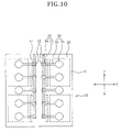
Referring to FIG. 10, after the first insulation layer pattern 20 is formed, redistribution line patterns 30 are formed on the first insulation layer pattern 20.
In order to form the redistribution line patterns 30, a metal layer (not shown) is formed on the entire area of the first insulation layer pattern 20. The metal layer can be formed through a chemical vapor deposition process or a sputtering process.
After the metal layer is formed, a photoresist film (not shown) is formed on the metal layer. The photoresist film can be formed, for example, through a spin coating process.
The photoresist film is patterned through a photo process including a lithographic process and a development process, by which a photoresist pattern is formed on the metal layer.
The metal layer is patterned using the photoresist pattern, and thereby, the redistribution line patterns 30 are formed on the first insulation layer pattern 20.
Each of the redistribution line patterns 30 formed on the first insulation layer pattern 20 has a pattern body 32 and a pad part 35. One end of the pattern body 32 is electrically connected with the bonding pad 12, and the pad part 35 is integrally formed with the other end of the pattern body 32, which faces away from the one end of the pattern body 32. In the present embodiment, the pattern body 32 is formed to have the shape of, for example, a line, and the pad part 35 is formed to have the shape of, for example, a disc.
Referring to FIG. 11, after the redistribution line patterns 30 are formed, a second pattern mask 300 is arranged on the first insulation layer pattern 20.
The second pattern mask 300 has a second mask body 305, second cover parts 310 and second connection parts 320.
The second mask body 305 has the shape of a quadrangular frame which has an opening for exposing at least a portion, preferably, the entire area of the first insulation layer pattern 20 of the semiconductor chip 10. The second cover parts 310 cover the respective pad parts 35 of the redistribution line patterns 30, and the second connection parts 320 connect the second cover parts 310. In the present embodiment, the second connection parts 320 have the shape of a line when viewed from the top.
After the second pattern mask 300 is arranged on the semiconductor chip 10, by applying an insulation material on the first insulation layer pattern 20 using the second pattern mask 300 and then removing the second pattern mask 300 from the first insulation layer pattern 20, the second insulation layer pattern 40, which exposes the pad parts 35 of the redistribution line patterns 30, is formed on the first insulation layer pattern 20 as shown in FIG. 12 without implementing a photo process.
In the present embodiment, the insulation material can be applied onto the first insulation layer pattern 20 by a screen printing method using a scraper 330. Unlike this, the insulation material can be applied onto the first insulation layer pattern 20 by a spraying method using an injection unit 340.
Referring again to FIG. 2, the second insulation layer pattern 40 has first open areas 43 which are defined by the second cover parts 310 of the second pattern mask 300 and expose the pad parts 35 of the redistribution line patterns 30, and second open areas 45 which are defined by the second connection parts 320 of the second pattern mask 300 and extend from the first open areas 43 to the edges of the semiconductor chip 10.
After the second insulation layer pattern 40 having the first and second open areas 43 and 45 is formed, conductive balls 50 such as solder balls are attached to the pad parts 35 of the redistribution line patterns 30, which are exposed through the first open areas 43, whereby the manufacture of the semiconductor package 100 is completed.
As is apparent from the above description, in the present invention, since processes for forming an insulation layer pattern to be used for forming redistribution line patterns connected with the bonding pads of a semiconductor chip and an insulation layer pattern to be used for insulating the redistribution line patterns can be simplified, the number of processes for manufacturing a semiconductor package can be significantly decreased.
Although specific embodiments of the present invention have been described for illustrative purposes, those skilled in the art will appreciate that various modifications, additions and substitutions are possible, without departing from the scope and the spirit of the invention as disclosed in the accompanying claims.

Claims (9)

1. A semiconductor package comprising:
a semiconductor chip having bonding pads;
a first insulation layer pattern having first openings exposing the bonding pads;
redistribution line patterns located on the first insulation layer pattern and electrically connected with the bonding pads;
a second insulation layer pattern covering the redistribution line patterns and having second openings which have first open areas exposing portions of the redistribution line patterns and second open areas extending away from the first open areas to edges of the semiconductor chip, wherein the second open areas expose portions of the first insulation layer pattern; and
conductive balls electrically connected with the portions of the redistribution line patterns which are exposed through the first open areas of the second insulation layer pattern.
2. The semiconductor package according to claim 1, wherein each redistribution line pattern includes a pattern body connected with one of the bonding pads and a pad part formed on an end of the pattern body, and one of the first opening areas exposing the pad part.
3. The semiconductor package according to claim 2, wherein the pad part having a disc shape, and each first open area having a circular shape and exposing a center portion of the pad part.
4. The semiconductor package according to claim 2, wherein each second open area having a direction which is substantially perpendicular to the pattern body.
5. The semiconductor package according to claim 2, wherein the second open areas extend from the first open areas along a portion of the semiconductor chip opposite to a portion of the semiconductor chip on which the pattern bodies extend such that at least a portion of the second open areas does not overlap the redistribution line patterns.
6. The semiconductor package according to claim 1, wherein each second open area having a slit shape when viewed from the top.
7. The semiconductor package according to claim 1, wherein each first opening having a first open region exposing one of the bonding pads and a second open region extending from the first open region toward an edge of the semiconductor chip.
8. The semiconductor package according to claim 7, wherein each second open region having a slit shape when viewed from the top.
9. The semiconductor package according to claim 1, wherein the second open areas extend from the first open areas and along a portion of the semiconductor chip not overlapping the redistribution line to edges of the semiconductor chip.
US12/044,178 2007-07-27 2008-03-07 Semiconductor package and method for manufacturing the same for decreasing number of processes Active 2028-03-16 US7732931B2 (en)

Priority Applications (1)

Application Number Priority Date Filing Date Title
US12/765,221 US7923294B2 (en) 2007-07-27 2010-04-22 Semiconductor package and method for manufacturing the same for decreasing number of processes

Applications Claiming Priority (2)

Application Number Priority Date Filing Date Title
KR10-2007-0076020 2007-07-27
KR1020070076020A KR100886710B1 (en) 2007-07-27 2007-07-27 Semiconductor package and manufacturing method thereof

Related Child Applications (1)

Application Number Title Priority Date Filing Date
US12/765,221 Division US7923294B2 (en) 2007-07-27 2010-04-22 Semiconductor package and method for manufacturing the same for decreasing number of processes

Publications (2)

Publication Number Publication Date
US20090026613A1 US20090026613A1 (en) 2009-01-29
US7732931B2 true US7732931B2 (en) 2010-06-08

Family

ID=40294541

Family Applications (2)

Application Number Title Priority Date Filing Date
US12/044,178 Active 2028-03-16 US7732931B2 (en) 2007-07-27 2008-03-07 Semiconductor package and method for manufacturing the same for decreasing number of processes
US12/765,221 Active US7923294B2 (en) 2007-07-27 2010-04-22 Semiconductor package and method for manufacturing the same for decreasing number of processes

Family Applications After (1)

Application Number Title Priority Date Filing Date
US12/765,221 Active US7923294B2 (en) 2007-07-27 2010-04-22 Semiconductor package and method for manufacturing the same for decreasing number of processes

Country Status (2)

Country Link
US (2) US7732931B2 (en)
KR (1) KR100886710B1 (en)

Families Citing this family (1)

* Cited by examiner, † Cited by third party
Publication number Priority date Publication date Assignee Title
DE102008064428B4 (en) * 2008-12-22 2016-02-25 Austriamicrosystems Ag Chip structure and method for producing a chip structure

Citations (5)

* Cited by examiner, † Cited by third party
Publication number Priority date Publication date Assignee Title
US20020185721A1 (en) 1999-09-30 2002-12-12 Chan Seung Hwang Chip size package having concave pattern in the bump pad area of redistribution patterns and method for manufacturing the same
US20040041166A1 (en) * 2002-08-28 2004-03-04 Morrison Michael W. Ball grid array structures and tape-based method of manufacturing same
KR20060036881A (en) 2004-10-26 2006-05-02 어드벤스드 칩 엔지니어링 테크놀로지, 인크. Chip-Size Package Structures and Manufacturing Method Thereof
KR20070104919A (en) 2005-02-24 2007-10-29 에이저 시스템즈 인크 Structure and method for manufacturing flip chip device
US7321164B2 (en) * 2005-08-15 2008-01-22 Phoenix Precision Technology Corporation Stack structure with semiconductor chip embedded in carrier

Patent Citations (5)

* Cited by examiner, † Cited by third party
Publication number Priority date Publication date Assignee Title
US20020185721A1 (en) 1999-09-30 2002-12-12 Chan Seung Hwang Chip size package having concave pattern in the bump pad area of redistribution patterns and method for manufacturing the same
US20040041166A1 (en) * 2002-08-28 2004-03-04 Morrison Michael W. Ball grid array structures and tape-based method of manufacturing same
KR20060036881A (en) 2004-10-26 2006-05-02 어드벤스드 칩 엔지니어링 테크놀로지, 인크. Chip-Size Package Structures and Manufacturing Method Thereof
KR20070104919A (en) 2005-02-24 2007-10-29 에이저 시스템즈 인크 Structure and method for manufacturing flip chip device
US7321164B2 (en) * 2005-08-15 2008-01-22 Phoenix Precision Technology Corporation Stack structure with semiconductor chip embedded in carrier

Also Published As

Publication number Publication date
US20090026613A1 (en) 2009-01-29
US20100203720A1 (en) 2010-08-12
US7923294B2 (en) 2011-04-12
KR100886710B1 (en) 2009-03-04
KR20090011953A (en) 2009-02-02

Similar Documents

Publication Publication Date Title
US8203217B2 (en) Semiconductor package having a stacked wafer level package and method for fabricating the same
US7825504B2 (en) Semiconductor package and multi-chip semiconductor package using the same
US7939947B2 (en) Semiconductor package structure
US8222083B2 (en) Semiconductor package adapted for high-speed data processing and damage prevention of chips packaged therein and method for fabricating the same
JP2006032556A (en) Semiconductor device and manufacturing method thereof
US7196000B2 (en) Method for manufacturing a wafer level chip scale package
JP5086115B2 (en) Wafer level semiconductor package and manufacturing method thereof
KR100959604B1 (en) Wafer level semiconductor package and method for manufacturing same
US20070228581A1 (en) Universal chip package structure
US7923294B2 (en) Semiconductor package and method for manufacturing the same for decreasing number of processes
US7638365B2 (en) Stacked chip package and method for forming the same
US8847377B2 (en) Stacked wafer level package having a reduced size
JP2008235573A (en) Semiconductor device and manufacturing method thereof
KR20180071476A (en) Method for manufacturing a fan-out wafer level semiconductor package
US20260026370A1 (en) Semiconductor package with stacked structure
KR100891530B1 (en) Semiconductor package and manufacturing method thereof
KR101013549B1 (en) Laminated Semiconductor Package and Method of Manufacturing the Same
KR100324602B1 (en) A manufacturing method of a semiconductor device capable of one-time package processing
KR20090096186A (en) Wafer level package and manufacturing method thereof
KR20080112628A (en) Semiconductor package and manufacturing method thereof
KR20080074652A (en) Semiconductor Chip Mounting Board

Legal Events

Date Code Title Description
AS Assignment

Owner name: HYNIX SEMICONDUCTOR INC., KOREA, REPUBLIC OF

Free format text: ASSIGNMENT OF ASSIGNORS INTEREST;ASSIGNOR:SUH, MIN SUK;REEL/FRAME:020615/0307

Effective date: 20080225

Owner name: HYNIX SEMICONDUCTOR INC.,KOREA, REPUBLIC OF

Free format text: ASSIGNMENT OF ASSIGNORS INTEREST;ASSIGNOR:SUH, MIN SUK;REEL/FRAME:020615/0307

Effective date: 20080225

FEPP Fee payment procedure

Free format text: PAYOR NUMBER ASSIGNED (ORIGINAL EVENT CODE: ASPN); ENTITY STATUS OF PATENT OWNER: LARGE ENTITY

STCF Information on status: patent grant

Free format text: PATENTED CASE

FPAY Fee payment

Year of fee payment: 4

FPAY Fee payment

Year of fee payment: 8

MAFP Maintenance fee payment

Free format text: PAYMENT OF MAINTENANCE FEE, 12TH YEAR, LARGE ENTITY (ORIGINAL EVENT CODE: M1553); ENTITY STATUS OF PATENT OWNER: LARGE ENTITY

Year of fee payment: 12