US7732302B2 - Integrated sensor and circuitry and process therefor - Google Patents
Integrated sensor and circuitry and process therefor Download PDFInfo
- Publication number
- US7732302B2 US7732302B2 US12/033,395 US3339508A US7732302B2 US 7732302 B2 US7732302 B2 US 7732302B2 US 3339508 A US3339508 A US 3339508A US 7732302 B2 US7732302 B2 US 7732302B2
- Authority
- US
- United States
- Prior art keywords
- wafer
- layer
- portions
- sensing structure
- bonding
- Prior art date
- Legal status (The legal status is an assumption and is not a legal conclusion. Google has not performed a legal analysis and makes no representation as to the accuracy of the status listed.)
- Expired - Fee Related, expires
Links
Images


Classifications
-
- G—PHYSICS
- G01—MEASURING; TESTING
- G01P—MEASURING LINEAR OR ANGULAR SPEED, ACCELERATION, DECELERATION, OR SHOCK; INDICATING PRESENCE, ABSENCE, OR DIRECTION, OF MOVEMENT
- G01P15/00—Measuring acceleration; Measuring deceleration; Measuring shock, i.e. sudden change of acceleration
- G01P15/18—Measuring acceleration; Measuring deceleration; Measuring shock, i.e. sudden change of acceleration in two or more dimensions
-
- B—PERFORMING OPERATIONS; TRANSPORTING
- B81—MICROSTRUCTURAL TECHNOLOGY
- B81C—PROCESSES OR APPARATUS SPECIALLY ADAPTED FOR THE MANUFACTURE OR TREATMENT OF MICROSTRUCTURAL DEVICES OR SYSTEMS
- B81C1/00—Manufacture or treatment of devices or systems in or on a substrate
- B81C1/00015—Manufacture or treatment of devices or systems in or on a substrate for manufacturing microsystems
- B81C1/00222—Integrating an electronic processing unit with a micromechanical structure
- B81C1/00253—Processes for integrating an electronic processing unit with a micromechanical structure not provided for in B81C1/0023 - B81C1/00246
-
- G—PHYSICS
- G01—MEASURING; TESTING
- G01C—MEASURING DISTANCES, LEVELS OR BEARINGS; SURVEYING; NAVIGATION; GYROSCOPIC INSTRUMENTS; PHOTOGRAMMETRY OR VIDEOGRAMMETRY
- G01C19/00—Gyroscopes; Turn-sensitive devices using vibrating masses; Turn-sensitive devices without moving masses; Measuring angular rate using gyroscopic effects
- G01C19/56—Turn-sensitive devices using vibrating masses, e.g. vibratory angular rate sensors based on Coriolis forces
- G01C19/5719—Turn-sensitive devices using vibrating masses, e.g. vibratory angular rate sensors based on Coriolis forces using planar vibrating masses driven in a translation vibration along an axis
-
- G—PHYSICS
- G01—MEASURING; TESTING
- G01P—MEASURING LINEAR OR ANGULAR SPEED, ACCELERATION, DECELERATION, OR SHOCK; INDICATING PRESENCE, ABSENCE, OR DIRECTION, OF MOVEMENT
- G01P1/00—Details of instruments
- G01P1/02—Housings
- G01P1/023—Housings for acceleration measuring devices
-
- G—PHYSICS
- G01—MEASURING; TESTING
- G01P—MEASURING LINEAR OR ANGULAR SPEED, ACCELERATION, DECELERATION, OR SHOCK; INDICATING PRESENCE, ABSENCE, OR DIRECTION, OF MOVEMENT
- G01P15/00—Measuring acceleration; Measuring deceleration; Measuring shock, i.e. sudden change of acceleration
- G01P15/02—Measuring acceleration; Measuring deceleration; Measuring shock, i.e. sudden change of acceleration by making use of inertia forces using solid seismic masses
- G01P15/08—Measuring acceleration; Measuring deceleration; Measuring shock, i.e. sudden change of acceleration by making use of inertia forces using solid seismic masses with conversion into electric or magnetic values
- G01P15/0802—Details
-
- G—PHYSICS
- G01—MEASURING; TESTING
- G01P—MEASURING LINEAR OR ANGULAR SPEED, ACCELERATION, DECELERATION, OR SHOCK; INDICATING PRESENCE, ABSENCE, OR DIRECTION, OF MOVEMENT
- G01P15/00—Measuring acceleration; Measuring deceleration; Measuring shock, i.e. sudden change of acceleration
- G01P15/02—Measuring acceleration; Measuring deceleration; Measuring shock, i.e. sudden change of acceleration by making use of inertia forces using solid seismic masses
- G01P15/08—Measuring acceleration; Measuring deceleration; Measuring shock, i.e. sudden change of acceleration by making use of inertia forces using solid seismic masses with conversion into electric or magnetic values
- G01P15/125—Measuring acceleration; Measuring deceleration; Measuring shock, i.e. sudden change of acceleration by making use of inertia forces using solid seismic masses with conversion into electric or magnetic values by capacitive pick-up
-
- B—PERFORMING OPERATIONS; TRANSPORTING
- B81—MICROSTRUCTURAL TECHNOLOGY
- B81B—MICROSTRUCTURAL DEVICES OR SYSTEMS, e.g. MICROMECHANICAL DEVICES
- B81B2201/00—Specific applications of microelectromechanical systems
- B81B2201/02—Sensors
- B81B2201/0228—Inertial sensors
- B81B2201/0235—Accelerometers
-
- B—PERFORMING OPERATIONS; TRANSPORTING
- B81—MICROSTRUCTURAL TECHNOLOGY
- B81C—PROCESSES OR APPARATUS SPECIALLY ADAPTED FOR THE MANUFACTURE OR TREATMENT OF MICROSTRUCTURAL DEVICES OR SYSTEMS
- B81C2201/00—Manufacture or treatment of microstructural devices or systems
- B81C2201/01—Manufacture or treatment of microstructural devices or systems in or on a substrate
- B81C2201/0174—Manufacture or treatment of microstructural devices or systems in or on a substrate for making multi-layered devices, film deposition or growing
- B81C2201/019—Bonding or gluing multiple substrate layers
-
- H—ELECTRICITY
- H01—ELECTRIC ELEMENTS
- H01L—SEMICONDUCTOR DEVICES NOT COVERED BY CLASS H10
- H01L2224/00—Indexing scheme for arrangements for connecting or disconnecting semiconductor or solid-state bodies and methods related thereto as covered by H01L24/00
- H01L2224/01—Means for bonding being attached to, or being formed on, the surface to be connected, e.g. chip-to-package, die-attach, "first-level" interconnects; Manufacturing methods related thereto
- H01L2224/42—Wire connectors; Manufacturing methods related thereto
- H01L2224/47—Structure, shape, material or disposition of the wire connectors after the connecting process
- H01L2224/48—Structure, shape, material or disposition of the wire connectors after the connecting process of an individual wire connector
- H01L2224/4805—Shape
- H01L2224/4809—Loop shape
- H01L2224/48091—Arched
-
- H—ELECTRICITY
- H01—ELECTRIC ELEMENTS
- H01L—SEMICONDUCTOR DEVICES NOT COVERED BY CLASS H10
- H01L2224/00—Indexing scheme for arrangements for connecting or disconnecting semiconductor or solid-state bodies and methods related thereto as covered by H01L24/00
- H01L2224/73—Means for bonding being of different types provided for in two or more of groups H01L2224/10, H01L2224/18, H01L2224/26, H01L2224/34, H01L2224/42, H01L2224/50, H01L2224/63, H01L2224/71
- H01L2224/732—Location after the connecting process
- H01L2224/73251—Location after the connecting process on different surfaces
- H01L2224/73265—Layer and wire connectors
-
- H—ELECTRICITY
- H01—ELECTRIC ELEMENTS
- H01L—SEMICONDUCTOR DEVICES NOT COVERED BY CLASS H10
- H01L2924/00—Indexing scheme for arrangements or methods for connecting or disconnecting semiconductor or solid-state bodies as covered by H01L24/00
- H01L2924/15—Details of package parts other than the semiconductor or other solid state devices to be connected
- H01L2924/161—Cap
- H01L2924/1615—Shape
- H01L2924/16195—Flat cap [not enclosing an internal cavity]
-
- H—ELECTRICITY
- H01—ELECTRIC ELEMENTS
- H01L—SEMICONDUCTOR DEVICES NOT COVERED BY CLASS H10
- H01L2924/00—Indexing scheme for arrangements or methods for connecting or disconnecting semiconductor or solid-state bodies as covered by H01L24/00
- H01L2924/15—Details of package parts other than the semiconductor or other solid state devices to be connected
- H01L2924/161—Cap
- H01L2924/162—Disposition
- H01L2924/16235—Connecting to a semiconductor or solid-state bodies, i.e. cap-to-chip
Definitions
- the present invention generally relates to micromachined semiconductor sensors and their fabrication. More particularly, this invention relates to a sensor comprising a capacitive sensing device capable of exhibiting large mechanical sensitivity and integration with circuitry to reduce input parasitics and improve the overall signal-to-noise ratio. The invention also relates to a manufacturing process by which such a sensing device and circuitry associated therewith can be fabricated on separate substrates prior to their integration.
- Motion sensors in the form of microelectromechanical system are widely used in aerospace and automotive safety control systems and navigational systems, consumer goods such as VCR cameras, as well as other mass-volume applications in which both performance and miniaturization is highly desirable and sometimes necessary.
- Capacitive micro-accelerometers have the combined advantages of high sensitivity, good direct current (dc) response and noise performance, low drift, low temperature sensitivity, low power dissipation, and large readout bandwidth as compared to high sensitivity tunneling and resonant devices.
- High sensitivity in capacitive accelerometers is attained in part by using a wafer-thick large proof mass. The first generation of these devices used multiple wafer bonding to form the proof mass and electrodes.
- capacitive accelerometers have been fabricated using a combined surface-bulk micromachining process to form the device on a single silicon wafer, such that the micromachined accelerometer is advantageously monolithically fabricated with the interface circuit. All of these devices are hybrid packaged with the interface circuitry, and as such are characterized by relatively large parasitics. A large capacitive sensitivity is generally used to compensation for the relatively high electrical noise floor caused by the parasitics. However, the proof mass of a surface micromachined accelerometer is typically small, which results in lower sensitivity and a mechanical noise floor of typically tens to hundreds of micro-g's.
- a capacitive micro-accelerometer could be fabricated that provides both large mechanical sensitivity and integration with CMOS circuitry to reduce input parasitics and improve the overall signal-to-noise ratio.
- CMOS circuitry to reduce input parasitics and improve the overall signal-to-noise ratio.
- the present invention provides a micromachined sensor and process for its fabrication, in which the sensor is capable of large mechanical sensitivity and integration with circuitry to reduce input parasitics and improve the overall signal-to-noise ratio of the sensor.
- a process is provided by which a micromachined sensor is formed to comprise a sensing structure and circuitry electrically coupled to the sensing structure.
- the process includes processing a first wafer to incompletely define the sensing structure in a first surface thereof, processing a second wafer to define the circuitry on a surface thereof, bonding the first and second wafers together, and then etching the first wafer to complete the sensing structure by removing portions of the first wafer at a second surface thereof opposite the first surface to define a member and by removing portions of the first wafer at the first surface thereof to release the member relative to the second wafer.
- a micromachined sensor having a capacitive sensing structure that includes a member comprising first and second conductive layers and a buried insulator layer separating the first and second conductive layers.
- a first set of elements is defined with the first conductive layer and comprises at least first and second elements that are electrically isolated from each other on the member by the buried insulator layer.
- a second set of elements is capacitively coupled with the first set of elements with gaps therebetween, and the capacitive couples generate capacitive outputs that vary with changes in the gaps.
- the first and second sets of elements define a symmetric capacitive full-bridge structure, with elements of the first set of elements being electrically insulated from each other by the insulator layer.
- the micromachined sensor comprises interface circuitry that includes means for performing multiple correlated double sampling of input thereto and output thereof, and means for performing chopper stabilization that reduces dc and low-frequency noise and drift.
- the sensor and process of this invention are applicable to a variety of MEMS structures, including accelerometers and other motion sensors.
- the invention can also be extended to sensing units with multiple sensors, such as integrated three-axis accelerometers and gyroscopes, and multiple-layer bonding for other MEMS structures such as micro-mirrors.
- the manner by which the process of this invention provides for vertical integration of a sensor and circuitry makes possible an integrated sensor of very small die size with multiple low-parasitics local leads between the sensor and its circuitry, which also simplifies packaging and reduces costs.
- the conductor-insulator-conductor (e.g., a silicon-on-insulator) construction employed by the micromachined sensor facilitates the fabrication of the preferred symmetric capacitive full-bridge structure, which enables precision readout without need for reference capacitors.
- the conductor-insulator-conductor e.g., a silicon-on-insulator construction employed by the micromachined sensor facilitates the fabrication of the preferred symmetric capacitive full-bridge structure, which enables precision readout without need for reference capacitors.
- FIG. 1 schematically represents a perspective view of a motion sensor comprising an integrated accelerometer and interface circuitry in accordance with the present invention.
- FIGS. 2 and 3 are top and bottom vies of an accelerometer sense element of the motions sensor of FIG. 1 .
- FIGS. 4 through 11 represent steps in the fabrication of the motion sensor of FIG. 1 .
- FIG. 12 is a simplified block diagram of the accelerometer and interface circuit of FIG. 1 .
- FIG. 13 is a simplified block diagram of the accelerometer and interface circuit with programmable output bandwidth.
- FIG. 14 is a schematic of a low-noise capacitance readout front-end circuit for use with the accelerometer and interface circuit of FIG. 1 .
- FIGS. 15 through 17 represent steps of a wafer-level packaging process for the motion sensor of FIG. 1 .
- FIG. 18 represents the motion sensor packaged within a sensor module.
- FIG. 19 schematically represents a perspective view of a sensor that includes the motion sensor of FIG. 1 combined with a z-axis gyroscope in accordance with an optional aspect of the present invention.
- FIG. 20 represents a cross-sectional view of the sensor of FIG. 19 .
- FIG. 21 represents steps in the fabrication of the sensor of FIGS. 19 and 20 .
- FIG. 22 schematically represents a perspective view of an alternative motion sensor in accordance with the present invention.
- FIGS. 23 and 24 represent steps in a fabrication process for a multiple level sensor in accordance with a further aspect of the present invention.
- FIGS. 25 and 26 represent steps in another fabrication process for a multiple level sensor in accordance with the present invention.
- FIG. 1 is a perspective view of a sensor device 10 in accordance with an embodiment of the invention.
- the sensor device 10 is a microelectromechanical system (MEMS) comprising a capacitive sensing element 12 supported above a substrate 16 .
- Circuitry 18 preferably CMOS interface circuitry
- the sensing element 12 includes a proof mass 14 with an in-plane axis of sensitivity, i.e., the plane of sensitivity is substantially parallel to the surface of the substrate 16 .
- the sensing element 12 is preferably responsive to lateral motion or acceleration, though capacitive sensing for other purposes is also within the scope of this invention. As such, while the invention will be described with particular reference to a capacitive acceleration sensor device 10 , the invention also encompasses other MEM's sensors and actuators. The relative sizes of structural components of the sensor device 10 are for illustrative purposes only.
- the mechanical structure of the sensor device 10 is preferably fabricated from single-crystal silicon, whose very stable mechanical characteristics promote higher sensor stability and manufacturing yield.
- the proof mass 14 is shown as being suspended over the substrate 16 with support beams 32 that generally limit the proof mass 14 to bidirectional movement.
- the beams 32 are shown having a folded configuration that enables the beams 32 to exhibit high stability over a wide temperature range.
- the folded support beams 32 have the further advantage of not being affected by limited residual thermo-mechanical stresses induced by dielectric and metal layers of the CMOS process on the substrate 16 .
- the proof mass 14 could be supported with other forms of suspension, including straight support beams to achieve lower cross-axis sensitivity.
- Sensing and feedback electrodes 20 electrically couple the sensing element 12 to the interface circuitry 18 on the substrate 16 .
- the electrodes 20 comprise pairs of interdigitated fingers 22 and 24 , one set of which extends from the proof mass 14 while the second set extends from anchors 26 on the substrate 16 .
- the fingers 22 and 24 are capacitively coupled in groups, with four isolated capacitive coupled groups (C s1+ , C s1 ⁇ , C s2+ , C s2 ⁇ ) being represented, though different numbers of capacitive couples are also within the scope of the invention. As represented in FIG.
- the interdigitated fingers 22 and 24 form a symmetrical full-bridge structure that helps to lower any potential residual effects of thermo-mechanical stresses in the substrate 16 .
- the support beams 32 of the proof mass 14 include bond pads 33 that provide electrical interconnection between the proof mass 14 , proof mass fingers 22 and the substrate 16 , as will be discussed in more detail in reference to FIGS. 2 and 3 .
- Electrical connections between the fixed fingers 24 and the substrate 16 are provided with bonding pads 34 formed beneath the anchors 26 by metal bonds, which do not adversely impact device performance due to their rigid connection to the substrate 16 .
- the fingers 22 and 24 are thick (e.g., a few micrometers to several hundred micrometers) and separated by relative narrow air gaps 28 (e.g., submicron to a few micrometers).
- the fingers 22 and 24 and air gaps 28 therebetween are preferably defined by front-side high aspect ratio deep reactive ion etching (DRIE), as will be discussed in more detail below.
- DRIE deep reactive ion etching
- the sensing element 12 is completed after integration with the substrate 16 on which the CMOS interface circuitry 18 was previously fabricated to achieve a high-yield batch CMOS-MEMS manufacturing process.
- the sensing element 12 is initially fabricated on a separate sensor wafer 30 ( FIGS. 4 through 6 ), and the proof mass 14 is formed and released by a final etch step after bonding the sensor wafer 30 to the substrate 16 , such as with a low-temperature wafer bonding process.
- the vertical integration of the sensing element 12 and its circuitry 18 made possible with the present invention provides multiple low-parasitic leads between the sensing element 12 and circuitry 18 , achieved through the electrical interconnections formed by the anchors 26 and beams 32 located in close proximity to the interface circuitry 18 on the substrate 16 .
- the vertical integration of the sensing element 12 and its circuitry 18 also provides the potential for reducing the size of the device 10 , simplify packaging, and reduce cost. Consecutive multiple wafer bonds and release etches can be used to form multilevel MEM's structures in combination with the sensing element 12 and CMOS substrate 16 .
- the sensor device 10 uses a capacitive sense scheme, which has the advantage of good dc response, high-sensitivity, low-noise, and low-temperature drift.
- squeeze film damping is the dominant regime for parallel fingers 22 and 24 whose widths and lengths are significantly larger than the air gap 28 .
- the symmetric capacitive full-bridge structure formed by the interdigitated fingers 22 and 24 is able to directly interface with a fully-differential readout front-end circuit ( FIG. 14 ) without any need for reference capacitors.
- the full-bridge structure also improves the overall sensitivity of the sensor device 10 and lowers drift including temperature sensitivity.
- the fingers 22 and 24 require multiple isolated leads to provide for the multiple sense capacitors indicated in FIG. 1 .
- a notable advantage of the sensor device 10 and fabrication process of this invention is the capability of simultaneously providing isolated sense capacitors and a full capacitance bridge. This aspect of the invention is more readily evident from FIGS.
- FIGS. 4 through 6 show the sensing element 12 (including the fingers 22 and 24 , anchors 26 , and beams 32 ) as being fabricated from a silicon-on-insulator (SOI) wafer 30 .
- the sensor fingers 22 extending from the proof mass 14 are formed by etching a first conductive (device) layer 36 of the wafer 30 , which is separated from a second conductive (handle) layer 38 of the wafer 30 by an insulative buried oxide layer 40 .
- the sensor fingers 22 are preferably formed by front-side high aspect ratio etching to have thicknesses of a few micrometers to several hundred micrometers, and air gaps 28 with widths as little as submicron size to a few micrometers.
- the thicker handle layer 38 of the wafer 30 is subsequently used to define the proof mass 14 . Because the device and handle layers 36 and 38 are electrically isolated from each other by the buried oxide layer 40 , trenches 41 can be etched in the device layer 36 during the same step used to define the sensor fingers 22 to delineate leads 42 on the lower surface of the proof mass 14 that are electrically isolated on the proof mass 14 by the buried oxide layer 40 , as shown in FIG. 4 .
- the buried oxide layer 40 structurally delineates a symmetrical full-bridge structure that is formed by the interdigitated fingers 22 and 24 and whose line of symmetry passes along an exposed portion of the buried oxide layer 40 , passes through the center of the proof mass 14 , and separates the beams 32 on the same side of the proof mass 14 .
- the finger gaps 28 are asymmetrical (g 0 >g s in FIG. 2 ) to provide a net capacitance change when the proof mass 14 and its fingers 22 are displaced relative to the fixed fingers 24 . For g 0 >4 g s the capacitance sensitivity is reduced by only about 6% compared with the case where a sensing element is formed by two parallel plates separated by a gap of g s .
- trenches with various shapes could be defined in the device layer 36 to electrically separate each lead 42 and its respective fingers 22 from the other leads 42 and their respective fingers 22 .
- the trenches could be configured to minimize the size of the leads 42 for the purpose of minimizing the buildup of charge within the leads 42 .
- trenches could also be etched in the proof mass 14 to define proof mass portions coinciding with the leads 42 , and then each proof mass portion electrically coupled (e.g., with conductive vias) to their respective leads 42 to reduce the buildup of charge within the proof mass 14 .
- the cross-axis sensitivity of the sensor device 12 can be minimized by proper spring geometry design (including the use of straight support beams 32 ) and reducing the distance between the center of gravity of the proof mass 14 and the plane of the beams 32 by optimizing the ratio of the thickness of the proof mass 14 to the height of the beams 32 .
- This entails increasing the height of the beams 32 (and sensor fingers 22 and 24 ), which increases the sensitivity of the device 10 as well.
- increased beam and finger thickness also increases damping and mechanical noise, as evident from the second and third equations above. As such, an optimal design can be obtained by adjusting the air gap 28 while maintaining the mechanical and electrical noise floor low.
- the sensor device 10 of this invention is adapted to operate at atmospheric ambient pressures (and higher).
- Those skilled in the art will appreciate that higher sensitivity and resolution can be achieved by vacuum packaging the sensor device 10 .
- suitable performance for the sensor device 10 is believed to be very likely achievable without the need for vacuum packaging.
- the sensor device 10 of this invention is therefore capable of avoiding the higher costs and more demanding sealing requirements associated with vacuum micropackaging processes. Nevertheless, higher sensitivity and resolution sensors obtainable by vacuum packaging is an optional aspect of the invention.
- the fabrication and manufacturing process for the sensor device 10 will now be more fully described in reference to FIGS. 4 through 11 .
- the preferred sensor fabrication process is fully compatible with post-CMOS processing, and enables the sensing element 12 to be formed and integrated with its CMOS interface circuitry 18 .
- Preferred fabrication steps are also batch processes that can be performed at wafer level, and their combination is a high-yield process that can be performed in a standard MEMS fabrication facility.
- FIGS. 4 through 6 represent preferred fabrication steps for the sensing element 12 , in which two masking steps are performed on the SOI sensor wafer 30 .
- Preferred thicknesses for the device and handle layers 36 and 38 of the wafer 30 are about 5 to about 200 ⁇ m and about 300 to about 600 ⁇ m, respectively, though it should be understood that other thicknesses could be employed.
- a plating seed layer 44 has been deposited over which a photo resist material is deposited and patterned to form a mold 46 in which bonding metal stacks 48 are electroplated.
- suitable bonding sites can be formed using other deposition processes (e.g., metal evaporation, sputtering, etc.), or by silkscreening or printing to form bond sites for polymer-based bonds, or patterning, masking, and exposing suitable bond sites to an electrical field or ions prior to field-assisted bonding.
- the mold 46 and portions of the plating seed layer 44 beneath the mold 46 are then removed ( FIG. 5 ), followed by patterning and etching the device layer 36 with a high aspect ratio DRIE silicon etch to form the interdigitated fingers 22 and 24 , anchors 26 , and suspension beams 32 and yield the structure shown in FIG. 6 .
- the backside of the sensor wafer 30 may also be patterned at this time (e.g., using a silicon oxide or nitride mask) for subsequent use during etching of the proof mass 14 ( FIG. 11 ).
- FIGS. 7 through 9 represent fabrication steps for the substrate 16 , referred to at this process level as the CMOS wafer 16 , in which the interface circuitry 18 has already been fabricated. Processing of the wafer 16 also has two masking steps, the first of which involves depositing and patterning metal stacks for use as bonding pads 50 . Suitable metal layers for the bond pads 50 include nickel and gold, though it is foreseeable that other materials could be used. The pads 50 contact the CMOS pads (not shown), which will later provide electrical connection between the sensing element 12 and the interface circuitry 18 . As represented in FIG. 8 , hard and soft polyimide layers 52 and 54 may optionally be spun and baked on the surface of the wafer 16 and subsequently patterned to yield structures for containing the bond pads 50 as shown in FIG.
- FIGS. 7 through 9 also depict a metal bonding ring 56 for a package cap 60 ( FIGS. 15 through 17 ) as having also been formed on the CMOS wafer 16 .
- the polyimide layers 54 and 56 provide a mold for metal TLP or solder bonding of the package cap 60 to the sensor device 10 .
- the top soft layer 56 provides compliance and allows the application of pressure during bonding to improve the bonding yield for CMOS and sensor wafers 16 and 30 having dissimilar radii of curvature. The soft layer 56 can be removed from the process if the radius of curvature difference is small.
- the third and final series of preferred steps include a single masking step.
- the sensor wafer 30 is flipped and aligned with the bond pads 50 on the CMOS wafer 16 . Slight pressure is then applied while the wafers 16 and 30 are bonded to yield the structure shown in FIG. 10 .
- Preferred bonding temperatures depend on the bonding scheme and materials, though generally it is believed that temperatures below 420° C., and particularly below 380° C., are compatible with the CMOS wafer 16 .
- the CMOS and sensor wafers 16 and 30 can be bonded using various low-temperature bonding schemes, including but not limited to transient liquid phase (TLP) bonding, metal-metal thermo-compression bonding, solder bonding, eutectic bonding, glass frit bonding, ion-assisted wafer bonding, field-assisted bonding, polymer/epoxy based bonding, etc.
- TLP transient liquid phase
- metal-metal thermo-compression bonding solder bonding
- eutectic bonding glass frit bonding
- ion-assisted wafer bonding ion-assisted wafer bonding
- field-assisted bonding polymer/epoxy based bonding, etc.
- a TLP bond is formed between a thin metal interlayer having a relatively low melting temperature and a parent metal with a higher melting temperature. At the bond temperature, the metal interlayer melts, flows to the parent metal, and is completely consumed by the parent metal to form an inter
- the higher melting temperature of the intermetallic compound allows multiple back-to-back bonds to be performed using the same metal bond composition and temperature.
- the cap 60 can be bonded to the CMOS wafer 16 using the very same TLP process and composition used to perform the CMOS-sensor wafer bond.
- a number of different metal compositions can be used for TLP, including Au—In, Au—Sn, and Ni—Sn whose bond temperatures are all below 380° C. and are therefore compatible with post-CMOS processing.
- the final preferred processing step is to conduct a silicon DRIE at the backside (handle layer 38 ) of the sensor wafer 30 to define the proof mass 14 .
- Suitable patterning techniques are well known in the art and therefore will not be discussed in any detail here.
- Final release of the proof mass 14 is completed by a blanket dry etching (RIE) of the exposed buried oxide layer 40 everywhere except areas masked by the proof mass 14 , to yield the structure shown in FIG. 11 .
- RIE blanket dry etching
- all processing steps described above are low temperature and compatible with deep-submicron CMOS.
- all etching steps are preferably dry etch processes to avoid stiction and enhance the fabrication yield.
- the interface circuitry 18 of this invention is discussed in reference to FIGS. 12 through 14 .
- the interface circuitry 18 preferably provides a differential analog readout of the capacitance change for a sensor device 10 .
- the interface circuitry 18 further provides the ability to simultaneously read the capacitance, apply feedback, and provide direct digital output for a Type B sensor device 10 having higher bandwidth and linearity specifications, as well as a higher noise budget.
- FIG. 12 shows a simplified block diagram of the sensor device 10 , sensing element 12 , and interface circuitry 18 .
- the circuitry 18 can be used both in open-loop and closed-loop modes of operation.
- a preferred readout front-end circuit 58 ( FIG. 14 ) is a fully differential switched-capacitor (SC) charge integrator with active offset and 1/f noise cancellation.
- SC switched-capacitor
- a particularly advantageous aspect of the invention is that the offset and 1/f noise cancellation are shown in FIG. 14 as being achieved with multi-pass correlated double sampling (CDS) at input and output, in combination with chopper stabilization for switch residual mismatch cancellation (discussed below). CDS also compensates the front-end amplifier finite gain.
- CDS multi-pass correlated double sampling
- FIG. 13 is a block diagram for an alternative interface circuitry 18 that supports programmable output bandwidth and integrates the oversampled sigma-delta modulator decimation filter as well.
- the circuitry 18 In order to be able to clock the circuitry 18 sufficiently fast, switches in the charging path of the sensor large capacitances cannot be minimum size. This in return increases any residual offset due to the mismatches of the switches and their charge injection, and reduces the dc response precision. Therefore, the circuitry 18 is shown as also employing switch chopper-stabilization to cancel the offset caused by switch mismatches, and thus enhances the overall accelerometer quasi-static response.
- the term chopper stabilization broadly encompasses the technique of alternating switches and their associated signal paths in a fully-differential readout circuit configuration to cancel any offset or near-dc errors caused by the mismatch of the switches connected to the signal path, and is known and particularly effective for use in switched-capacitor circuits.
- the circuitry 18 also includes a digital servo compensator that employs pulse width modulation (PWM) to implement phase-lead compensation.
- PWM pulse width modulation
- the circuitry 18 is also shown as including a sensor start-up circuit that is activated at power down or recovery from over-range input.
- the circuitry 18 supplies additional electrostatic force in these cases and minimizes the supply voltage (Vsupply) requirements, which is typically desirable in consideration for the overall chip dynamic range and needed electrostatic force.
- Vsupply supply voltage
- the integrated CMOS-MEMS sensor device 10 of this invention offers higher resolution due to its integrated process and lower parasitics.
- the readout resolution of the circuitry 18 can be further increased by increasing the sampling rate.
- the lower parasitics also help with increasing the sampling clock by reducing the node capacitances.
- the dominant noise source is kT/C noise of the charge integration capacitor (which is typically the smallest capacitor affected by this noise source), and is due to sampling and aliasing the wide-bandwidth thermal noise of the circuit switches.
- kT/C noise cancellation is obtained with the output CDS noted above as part of the combination of multi-pass CDS and chopper stabilization.
- FIG. 14 shows the schematic for the preferred readout front-end circuit 58 .
- the dominant noise source becomes the sampled amplifier noise, which is significantly lower.
- the output CDS is implemented by adding capacitors C os+ and C os ⁇ that sample C int noise in clock phase ( ⁇ os ), and consequently deduct C int noise from the output.
- the circuit 58 utilizes switch chopper stabilization by alternating the switches at the high impedance nodes between the two differential signal paths.
- the front-end circuit 58 has three main clock phases: in the precharge phase ( ⁇ os ) the capacitive bridge is charged to the rails; in the charge integration phase ( ⁇ 1 ), the capacitive bridge is charged in the reverse direction and a packet of charge proportional to the sense capacitors difference is integrated on the feedback capacitors (C int ); in the feedback phase ( ⁇ f), the capacitive bridge is disconnected from the integrator input and electrostatic feedback bit is applied (closed-loop mode of operation).
- FIGS. 15 through 18 pertain to a packaging processes for the sensor device 10 .
- the sensor device 10 is encapsulated at wafer-level using a silicon cap 60 to provide protection from the environment prior to die singulation and handling.
- the sealed cap 60 also isolates the sensor device 10 from its operating environment, and can also provide isolation or protection from the ambient humidity and pressure variations.
- the silicon cap 60 and CTE matching can be effective in reducing thermal stresses in the device 10 .
- FIG. 15 represents a first step in the packaging process flow, in which bond metal stacks 62 are patterned and electroplated on a cap wafer 64 .
- the wafer 64 is then patterned and a cavity etch performed while the bond metal stacks 62 are protected (not shown) to yield the cap 60 shown in FIG. 16 .
- the cavity etch can be performed using wet anisotropic etching of silicon with (100) surface orientation to form the sloping sidewalls shown in FIG. 16 , or by dry etching or wet etching of (110) silicon to produce a cavity with nearly vertical sidewalls capable of reducing overall die size.
- the cap 60 is then flipped, aligned to the CMOS wafer 16 and a seal bond is performed, e.g., using solder or glass frit bonding, TLP, or another suitable low-temperature bonding scheme as described previously, preferably at a temperature of less than 300° C.
- the resulting capped sensor 66 can then be diced and packaged similar to a standard IC chip. It is worth noting that the CMOS-MEMS integration technique provided by this invention simplifies the packaging operation, since all leads for the sensor device 10 are connected to the CMOS substrate 16 locally through the beams 32 and anchors 26 , and no lead-transfer from the sensor device 10 to the exterior of the cap 60 is required.
- FIG. 18 schematically represents a packaged sensor module 68 in which the capped sensor 66 is contained and represented as being wire-bonded to a module housing 70 .
- the impact of the module housing 70 and its potential induced thermal stresses are preferably minimized, such as by appropriate choices of materials for the housing 70 , for example, ceramics or other materials whose coefficients of thermal expansion (CTE) are approximately matched to silicon, and/or proper die bond materials and stress isolation techniques for die attachments as known in the art.
- CTE coefficients of thermal expansion
- the symmetrical construction of the device 10 and use of the folded beam design depicted in FIGS. 1 through 3 serve to reduce or cancel the effect of package stresses on the sensor performance.
- FIGS. 19 and 20 schematically represent a sensor unit that includes the sensor device 10 of FIG. 1 combined with a z-axis gyroscope 72 .
- Suitable steps in the fabrication of the sensor unit of FIG. 19 are represented in FIG. 21 , and correspond to the processing steps depicted in FIGS. 4 through 11 .
- sensors with out-of-plane sensitivity are also within the scope of this invention, as evidenced by FIG. 22 .
- the same processing steps used to produce the sensor device 10 of FIG. 1 can be used to produce the sensor device 74 of FIG. 22 , whose primary components are numbered consistently with the corresponding components of the device 10 of FIG. 1 .
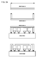
- FIGS. 23 through 26 illustrate the extension of the present invention to multiple level sensor structures.
- sensor and CMOS wafers are processed generally in the same manner as that represented in FIGS. 4 through 11 , and additional steps for fabricating and bonding a second sensor (MEMS) wafer to provide a second sensor level are represented in FIG. 24 .
- MEMS second sensor
- FIG. 25 represents processing of a sensor wafer in which the handle layer of the original SOI wafer is completely removed, with the additional steps for fabricating and bonding a second sensor (MEMS) wafer represented in FIG. 26 .
- both sensor wafers are SOI wafers.
- the device layer remains of the first SOI wafer within the first sensor level, while both device and handle layers of the second SOI wafer are present in the second sensor level of the multiple level sensor structure.
- the final dry etch could be eliminated, depending on the type of sensor being fabricated.
Abstract
Description
ΔC static /a=N(∈0 Am)/(g s 2 k)=N(∈0 A)/(g s 2ωr 2)
where ΔCstatic is the sensor capacitance change, a is the input acceleration, N is the number of pairs of
TNEA=(4K B TD)1/2 /m=(4K B Tω r)1/2
where KB is the Boltzmann constant, T is temperature in Kelvin, D is the damping factor, and Q is the quality factor. When not in a low-pressure ambient, squeeze film damping is the dominant regime for
D=0.427NμT 3 L/g s 3=0.427NμAT 2 /g s 3
Claims (18)
Priority Applications (1)
| Application Number | Priority Date | Filing Date | Title |
|---|---|---|---|
| US12/033,395 US7732302B2 (en) | 2005-07-21 | 2008-02-19 | Integrated sensor and circuitry and process therefor |
Applications Claiming Priority (3)
| Application Number | Priority Date | Filing Date | Title |
|---|---|---|---|
| US70130005P | 2005-07-21 | 2005-07-21 | |
| US11/458,729 US7562573B2 (en) | 2005-07-21 | 2006-07-20 | Integrated sensor and circuitry and process therefor |
| US12/033,395 US7732302B2 (en) | 2005-07-21 | 2008-02-19 | Integrated sensor and circuitry and process therefor |
Related Parent Applications (1)
| Application Number | Title | Priority Date | Filing Date |
|---|---|---|---|
| US11/458,729 Division US7562573B2 (en) | 2005-07-21 | 2006-07-20 | Integrated sensor and circuitry and process therefor |
Publications (2)
| Publication Number | Publication Date |
|---|---|
| US20080188059A1 US20080188059A1 (en) | 2008-08-07 |
| US7732302B2 true US7732302B2 (en) | 2010-06-08 |
Family
ID=38957275
Family Applications (3)
| Application Number | Title | Priority Date | Filing Date |
|---|---|---|---|
| US11/458,729 Active 2026-09-11 US7562573B2 (en) | 2005-07-21 | 2006-07-20 | Integrated sensor and circuitry and process therefor |
| US12/033,395 Expired - Fee Related US7732302B2 (en) | 2005-07-21 | 2008-02-19 | Integrated sensor and circuitry and process therefor |
| US12/368,691 Expired - Fee Related US7810394B2 (en) | 2005-07-21 | 2009-02-10 | Integrated sensor and circuitry |
Family Applications Before (1)
| Application Number | Title | Priority Date | Filing Date |
|---|---|---|---|
| US11/458,729 Active 2026-09-11 US7562573B2 (en) | 2005-07-21 | 2006-07-20 | Integrated sensor and circuitry and process therefor |
Family Applications After (1)
| Application Number | Title | Priority Date | Filing Date |
|---|---|---|---|
| US12/368,691 Expired - Fee Related US7810394B2 (en) | 2005-07-21 | 2009-02-10 | Integrated sensor and circuitry |
Country Status (2)
| Country | Link |
|---|---|
| US (3) | US7562573B2 (en) |
| WO (1) | WO2008010931A2 (en) |
Cited By (11)
| Publication number | Priority date | Publication date | Assignee | Title |
|---|---|---|---|---|
| US20090303204A1 (en) * | 2007-01-05 | 2009-12-10 | Invensense Inc. | Controlling and accessing content using motion processing on mobile devices |
| US20110018075A1 (en) * | 2009-07-23 | 2011-01-27 | Lung-Tai Chen | Structure and fabrication method of a sensing device |
| US8508039B1 (en) | 2008-05-08 | 2013-08-13 | Invensense, Inc. | Wafer scale chip scale packaging of vertically integrated MEMS sensors with electronics |
| US8539835B2 (en) | 2008-09-12 | 2013-09-24 | Invensense, Inc. | Low inertia frame for detecting coriolis acceleration |
| US8952832B2 (en) | 2008-01-18 | 2015-02-10 | Invensense, Inc. | Interfacing application programs and motion sensors of a device |
| US8960002B2 (en) | 2007-12-10 | 2015-02-24 | Invensense, Inc. | Vertically integrated 3-axis MEMS angular accelerometer with integrated electronics |
| US8997564B2 (en) | 2007-07-06 | 2015-04-07 | Invensense, Inc. | Integrated motion processing unit (MPU) with MEMS inertial sensing and embedded digital electronics |
| JP2018132506A (en) * | 2017-02-17 | 2018-08-23 | 株式会社日立製作所 | Acceleration sensor |
| US10213107B2 (en) | 2014-07-01 | 2019-02-26 | Injectsense, Inc. | Methods and devices for implantation of intraocular pressure sensors |
| US10973425B2 (en) | 2014-07-01 | 2021-04-13 | Injectsense, Inc. | Hermetically sealed implant sensors with vertical stacking architecture |
| US11287443B2 (en) * | 2019-02-20 | 2022-03-29 | Invensense, Inc. | High performance accelerometer |
Families Citing this family (92)
| Publication number | Priority date | Publication date | Assignee | Title |
|---|---|---|---|---|
| EP1811309B1 (en) * | 2006-01-20 | 2009-10-07 | STMicroelectronics S.r.l. | Free fall detector device and free fall detection method |
| US7454967B2 (en) * | 2006-07-10 | 2008-11-25 | Lv Sensors, Inc. | Signal conditioning methods and circuits for a capacitive sensing integrated tire pressure sensor |
| US7409862B2 (en) * | 2006-10-18 | 2008-08-12 | Honeywell International Inc. | Systems and methods for isolation of torque and sense capacitors of an accelerometer |
| US7851876B2 (en) * | 2006-10-20 | 2010-12-14 | Hewlett-Packard Development Company, L.P. | Micro electro mechanical system |
| US20090265671A1 (en) * | 2008-04-21 | 2009-10-22 | Invensense | Mobile devices with motion gesture recognition |
| GB0720412D0 (en) * | 2007-10-18 | 2007-11-28 | Melexis Nv | Combined mems accelerometer and gyroscope |
| DE102007050116B4 (en) | 2007-10-19 | 2023-08-03 | Robert Bosch Gmbh | accelerometer |
| US7880246B2 (en) * | 2007-11-29 | 2011-02-01 | Stichting Imec Nederland | Microstructure with enlarged mass and electrode area for kinetic to electrical energy conversion |
| FR2924856B1 (en) * | 2007-12-11 | 2012-02-10 | Memscap | CAPACITOR VARIABLE CAPACITOR COMPRISING A MOBILE COMB AND AN INTERMEDIATED FIXED COMB, ACCELEROMETER AND GYROMETER COMPRISING SUCH CAPACITOR |
| US8044792B2 (en) * | 2008-01-30 | 2011-10-25 | Hewlett-Packard Development Company, L.P. | System and method for controlling remote sensors |
| DE102008002809A1 (en) * | 2008-03-21 | 2009-09-24 | Patev Gmbh & Co. Kg | Micromechanical device for e.g. binoculars, has image processing units, and imaging element and position, orientation or movement detecting system that are mechanically and fixedly connected with each other at common component |
| US20090261416A1 (en) * | 2008-04-18 | 2009-10-22 | Wolfgang Raberg | Integrated mems device and control circuit |
| US8217475B2 (en) * | 2008-05-15 | 2012-07-10 | Custom Sensors & Technologies, Inc. | Backside controlled MEMS capacitive sensor and interface and method |
| US8020440B2 (en) * | 2008-05-16 | 2011-09-20 | Rosemount Aerospace Inc. | System and method for providing high-range capability with closed-loop inertial sensors |
| KR100986221B1 (en) * | 2008-06-16 | 2010-10-08 | 한국산업기술대학교산학협력단 | Apparatus for vertical accelerometer |
| US8187902B2 (en) * | 2008-07-09 | 2012-05-29 | The Charles Stark Draper Laboratory, Inc. | High performance sensors and methods for forming the same |
| EP2327960B1 (en) * | 2008-08-18 | 2019-10-09 | Hitachi, Ltd. | Micro electro mechanical system |
| US9128114B2 (en) * | 2008-09-15 | 2015-09-08 | Nxp, B.V. | Capacitive sensor device and a method of sensing accelerations |
| US8207586B2 (en) * | 2008-09-22 | 2012-06-26 | Alps Electric Co., Ltd. | Substrate bonded MEMS sensor |
| USD611855S1 (en) * | 2008-10-20 | 2010-03-16 | Alps Electric Co., Ltd. | Pressure sensor |
| JP2010249805A (en) * | 2009-03-26 | 2010-11-04 | Seiko Epson Corp | Mems sensor, mems sensor manufacturing method, and electronic device |
| TWI375146B (en) * | 2009-04-08 | 2012-10-21 | Wistron Corp | Electronic device |
| US8322225B2 (en) * | 2009-07-10 | 2012-12-04 | Honeywell International Inc. | Sensor package assembly having an unconstrained sense die |
| DE102009045696B4 (en) * | 2009-10-14 | 2021-06-02 | Robert Bosch Gmbh | Method for the capacitive detection of a mechanical deflection |
| US8230743B2 (en) | 2010-08-23 | 2012-07-31 | Honeywell International Inc. | Pressure sensor |
| US20120048019A1 (en) * | 2010-08-26 | 2012-03-01 | Hanqin Zhou | Highly sensitive capacitive sensor and methods of manufacturing the same |
| EP2428774B1 (en) | 2010-09-14 | 2013-05-29 | Stichting IMEC Nederland | Readout system for MEMs-based capacitive accelerometers and strain sensors, and method for reading |
| US8486744B2 (en) * | 2010-09-28 | 2013-07-16 | Taiwan Semiconductor Manufacturing Company, Ltd. | Multiple bonding in wafer level packaging |
| JP5104936B2 (en) | 2010-11-22 | 2012-12-19 | 株式会社デンソー | Acceleration and angular velocity detection device |
| US9227835B2 (en) * | 2010-11-23 | 2016-01-05 | Honeywell International Inc. | Vibration isolation interposer die |
| GB201020722D0 (en) | 2010-12-07 | 2011-01-19 | Atlantic Inertial Systems Ltd | Accelerometer |
| CN102183677B (en) * | 2011-03-15 | 2012-08-08 | 迈尔森电子(天津)有限公司 | Integrated inertial sensor and pressure sensor and forming method thereof |
| US20120255357A1 (en) * | 2011-04-08 | 2012-10-11 | Dongmin Chen | Sensor package having integrated accelerometer and magnetometer |
| US8866498B2 (en) * | 2011-08-29 | 2014-10-21 | Robert Bosch Gmbh | Surface charge reduction technique for capacitive sensors |
| TWI452297B (en) * | 2011-09-26 | 2014-09-11 | Richwave Technology Corp | Capacitive accelerometer |
| GB201117164D0 (en) | 2011-10-05 | 2011-11-16 | Atlantic Inertial Systems Ltd | Accelerometer |
| CN102435772B (en) * | 2011-10-14 | 2013-03-20 | 苏州文智芯微系统技术有限公司 | Micro-mechanical acceleration transducer with directly linked silicon wafers based on silicon through-hole technique |
| US8937807B2 (en) * | 2011-11-21 | 2015-01-20 | Emerson Network Power—Embedded Computing, Inc. | Circuit board heatsink and heatframe structures with heater element for circuit board operation at below zero temperature |
| ITTO20120154A1 (en) * | 2012-02-21 | 2013-08-22 | Stmicroelectronics Malta Ltd | ASSEMBLY PROCEDURE OF AN INTEGRATED DEVICE WITH SEMICONDUCTOR |
| CN102607543B (en) * | 2012-04-01 | 2014-12-24 | 苏州文智芯微系统技术有限公司 | Silicon wafer directly-bonded micro-mechanical gyroscope based on silicon through hole technology |
| US9003886B2 (en) * | 2012-04-27 | 2015-04-14 | Freescale Semiconductor, Inc. | Microelectromechanical systems devices and methods for the fabrication thereof |
| DE112012006296T5 (en) * | 2012-04-30 | 2015-01-22 | Hewlett-Packard Development Co., L.P. | Message based on an event identified from vibration data |
| WO2013165348A1 (en) * | 2012-04-30 | 2013-11-07 | Hewlett-Packard Development Company | Control signal based on a command tapped by a user |
| DE102012013096A1 (en) | 2012-06-30 | 2014-01-02 | X-Fab Semiconductor Foundries Ag | Method for manufacturing micro-electromechanical system (MEMS), involves forming electrical interconnections between cavity disc and circuitry disc, and enabling completion of element by standard methods and connection technique |
| KR102127100B1 (en) | 2012-07-26 | 2020-06-29 | 디퍼이 신테스 프로덕츠, 인코포레이티드 | Ycbcr pulsed illumination scheme in a light deficient environment |
| BR112015001555A2 (en) | 2012-07-26 | 2017-07-04 | Olive Medical Corp | continuous video in low light environment |
| WO2014020479A2 (en) * | 2012-08-03 | 2014-02-06 | Ecole Polytechnique Federale De Lausanne (Epfl) | Post-CMOS Processing and 3D Integration Based on Dry-Film Lithography |
| JP2014107779A (en) * | 2012-11-29 | 2014-06-09 | Seiko Epson Corp | Vibrator, manufacturing method of vibrator, electronic apparatus and mobile body |
| US10132630B2 (en) * | 2013-01-25 | 2018-11-20 | MCube Inc. | Multi-axis integrated MEMS inertial sensing device on single packaged chip |
| US10036635B2 (en) | 2013-01-25 | 2018-07-31 | MCube Inc. | Multi-axis MEMS rate sensor device |
| US10023459B2 (en) * | 2013-03-11 | 2018-07-17 | Taiwan Semiconductor Manufacturing Company, Ltd. | MEMS and method for forming the same |
| EP2967301B1 (en) | 2013-03-15 | 2021-11-03 | DePuy Synthes Products, Inc. | Scope sensing in a light controlled environment |
| WO2014145249A1 (en) | 2013-03-15 | 2014-09-18 | Olive Medical Corporation | Controlling the integral light energy of a laser pulse |
| US9061886B1 (en) * | 2013-03-15 | 2015-06-23 | Hrl Laboratories, Llc | Doubly-clamped bean quartz micro-resonator |
| EP2967294B1 (en) | 2013-03-15 | 2020-07-29 | DePuy Synthes Products, Inc. | Super resolution and color motion artifact correction in a pulsed color imaging system |
| DE102013007593B4 (en) | 2013-05-02 | 2022-12-29 | Northrop Grumman Litef Gmbh | ACCELERATION SENSOR AND METHOD FOR MANUFACTURING ACCELERATION SENSOR |
| KR101531093B1 (en) * | 2013-07-31 | 2015-06-23 | 삼성전기주식회사 | Acceleration Sensor and Angular Velocity Sensor |
| JP2015123526A (en) * | 2013-12-26 | 2015-07-06 | ソニー株式会社 | Function element, acceleration sensor, and switch |
| US9977097B1 (en) | 2014-02-21 | 2018-05-22 | Hrl Laboratories, Llc | Micro-scale piezoelectric resonating magnetometer |
| JP6573960B2 (en) * | 2014-03-21 | 2019-09-11 | デピュイ・シンセス・プロダクツ・インコーポレイテッド | Card edge connector for imaging sensors |
| US9991863B1 (en) | 2014-04-08 | 2018-06-05 | Hrl Laboratories, Llc | Rounded and curved integrated tethers for quartz resonators |
| JP6451076B2 (en) * | 2014-05-01 | 2019-01-16 | セイコーエプソン株式会社 | Functional elements, physical quantity sensors, electronic devices, and moving objects |
| JP6113686B2 (en) * | 2014-05-27 | 2017-04-12 | 株式会社豊田中央研究所 | MEMS device |
| CN105445495B (en) * | 2014-07-16 | 2018-11-02 | 中国科学院地质与地球物理研究所 | A kind of symmetrical MEMS acceleration sensitives chip and its manufacturing process |
| JP6358913B2 (en) * | 2014-09-30 | 2018-07-18 | 株式会社日立製作所 | Acceleration sensor |
| JP6262629B2 (en) | 2014-09-30 | 2018-01-17 | 株式会社日立製作所 | Inertial sensor |
| US9923545B2 (en) | 2014-10-22 | 2018-03-20 | Microchip Technology Incorporated | Compound spring MEMS resonators for frequency and timing generation |
| US9866200B2 (en) * | 2014-10-22 | 2018-01-09 | Microchip Technology Incorporated | Multiple coil spring MEMS resonator |
| US9613926B2 (en) * | 2014-12-26 | 2017-04-04 | Taiwan Semiconductor Manufacturing Company, Ltd. | Wafer to wafer bonding process and structures |
| US10031191B1 (en) | 2015-01-16 | 2018-07-24 | Hrl Laboratories, Llc | Piezoelectric magnetometer capable of sensing a magnetic field in multiple vectors |
| JP6372361B2 (en) * | 2015-01-16 | 2018-08-15 | 株式会社デンソー | Compound sensor |
| JP2016151738A (en) | 2015-02-19 | 2016-08-22 | ルネサスエレクトロニクス株式会社 | Semiconductor device, correction method in semiconductor device and correction method in camera module |
| US10082438B2 (en) * | 2015-04-30 | 2018-09-25 | Nxp Usa, Inc. | Multi-sensor system and method of forming same |
| US9419597B1 (en) * | 2015-06-15 | 2016-08-16 | Analog Devices Global | Power-efficient chopping scheme for offset error correction in MEMS gyroscopes |
| JP6657626B2 (en) * | 2015-07-10 | 2020-03-04 | セイコーエプソン株式会社 | Physical quantity sensors, electronic devices and moving objects |
| US9550668B1 (en) * | 2015-08-25 | 2017-01-24 | Globalfoundries Singapore Pte. Ltd. | Integrated MEMS pressure sensor and MEMS inertial sensor |
| US10175307B1 (en) | 2016-01-15 | 2019-01-08 | Hrl Laboratories, Llc | FM demodulation system for quartz MEMS magnetometer |
| DE102016109118A1 (en) | 2016-05-18 | 2017-11-23 | Infineon Technologies Ag | Circuit architecture for a measuring device, a level converter circuit, a charge pumping stage and a charge pump and method for operating these |
| DE102016109114A1 (en) | 2016-05-18 | 2017-11-23 | Infineon Technologies Ag | Circuit architecture for a measuring device, a level converter circuit, a charge pumping stage and a charge pump and method for operating these |
| US10696541B2 (en) | 2016-05-26 | 2020-06-30 | Honeywell International Inc. | Systems and methods for bias suppression in a non-degenerate MEMS sensor |
| US10371521B2 (en) | 2016-05-26 | 2019-08-06 | Honeywell International Inc. | Systems and methods for a four-mass vibrating MEMS structure |
| JP6691882B2 (en) | 2017-03-03 | 2020-05-13 | 株式会社日立製作所 | Acceleration sensor |
| US10859620B2 (en) * | 2017-04-04 | 2020-12-08 | The Charles Stark Draper Laboratory, Inc. | Miniature electric field detector |
| US10591318B2 (en) | 2017-08-31 | 2020-03-17 | Invensense, Inc. | Half-bridge circuit for a sensor |
| US11525870B2 (en) | 2017-10-05 | 2022-12-13 | The Charles Stark Draper Laboratory, Inc. | Electromagnetic gradiometers |
| US10816568B2 (en) | 2017-12-26 | 2020-10-27 | Physical Logic Ltd. | Closed loop accelerometer |
| JP7075849B2 (en) * | 2018-08-29 | 2022-05-26 | 株式会社日立製作所 | MEMS Capacitive Accelerometer |
| JP7188311B2 (en) * | 2019-07-31 | 2022-12-13 | セイコーエプソン株式会社 | Gyro sensors, electronic devices, and mobile objects |
| EP3839519B1 (en) * | 2019-12-18 | 2023-11-08 | Murata Manufacturing Co., Ltd. | Microelectromechanical device with stopper |
| EP4191318A4 (en) * | 2020-07-31 | 2024-01-17 | Fujifilm Corp | Optical scanning device, method for driving same, and image drawing system |
| DE102021201149A1 (en) | 2021-02-08 | 2022-08-11 | Robert Bosch Gesellschaft mit beschränkter Haftung | Readout circuit for a sensor system and sensor system |
| US11677337B2 (en) * | 2021-08-13 | 2023-06-13 | Aac Acoustic Technologies (Shenzhen) Co., Ltd. | Comb drive for microelectromechanical system |
Citations (10)
| Publication number | Priority date | Publication date | Assignee | Title |
|---|---|---|---|---|
| US5345824A (en) | 1990-08-17 | 1994-09-13 | Analog Devices, Inc. | Monolithic accelerometer |
| US5610335A (en) | 1993-05-26 | 1997-03-11 | Cornell Research Foundation | Microelectromechanical lateral accelerometer |
| US6277666B1 (en) | 1999-06-24 | 2001-08-21 | Honeywell Inc. | Precisely defined microelectromechanical structures and associated fabrication methods |
| US6313529B1 (en) * | 1997-08-08 | 2001-11-06 | Denso Corporation | Bump bonding and sealing a semiconductor device with solder |
| US6701788B2 (en) | 2001-07-31 | 2004-03-09 | Kelsey-Hayes Company | Multiple output inertial sensing device |
| US20040065638A1 (en) | 2002-10-07 | 2004-04-08 | Bishnu Gogoi | Method of forming a sensor for detecting motion |
| US6718605B2 (en) | 1997-09-08 | 2004-04-13 | The Regents Of The University Of Michigan | Single-side microelectromechanical capacitive accelerometer and method of making same |
| US6846724B2 (en) * | 2001-09-28 | 2005-01-25 | Rockwell Automation Technologies, Inc. | Method for fabricating a microelectromechanical system (MEMS) device using a pre-patterned bridge |
| US20060201249A1 (en) * | 2005-03-09 | 2006-09-14 | Horning Robert D | MEMS device with thinned comb fingers |
| US20080138922A1 (en) * | 1999-12-15 | 2008-06-12 | Chang-Feng Wan | Micro-electro mechanical device made from mono-crystalline silicon and method of manufacture therefore |
Family Cites Families (6)
| Publication number | Priority date | Publication date | Assignee | Title |
|---|---|---|---|---|
| DE4430439C2 (en) * | 1994-08-29 | 1997-12-11 | Litef Gmbh | Sensor unit with at least one rotation rate sensor and method for its production |
| US6291875B1 (en) * | 1998-06-24 | 2001-09-18 | Analog Devices Imi, Inc. | Microfabricated structures with electrical isolation and interconnections |
| US6868726B2 (en) * | 2000-01-20 | 2005-03-22 | Analog Devices Imi, Inc. | Position sensing with improved linearity |
| JP2002131331A (en) * | 2000-10-24 | 2002-05-09 | Denso Corp | Semiconductor dynamical quantity sensor |
| US7422928B2 (en) * | 2003-09-22 | 2008-09-09 | Matsushita Electric Works, Ltd. | Process for fabricating a micro-electro-mechanical system with movable components |
| US7337671B2 (en) * | 2005-06-03 | 2008-03-04 | Georgia Tech Research Corp. | Capacitive microaccelerometers and fabrication methods |
-
2006
- 2006-07-20 US US11/458,729 patent/US7562573B2/en active Active
-
2007
- 2007-07-10 WO PCT/US2007/015734 patent/WO2008010931A2/en active Search and Examination
-
2008
- 2008-02-19 US US12/033,395 patent/US7732302B2/en not_active Expired - Fee Related
-
2009
- 2009-02-10 US US12/368,691 patent/US7810394B2/en not_active Expired - Fee Related
Patent Citations (10)
| Publication number | Priority date | Publication date | Assignee | Title |
|---|---|---|---|---|
| US5345824A (en) | 1990-08-17 | 1994-09-13 | Analog Devices, Inc. | Monolithic accelerometer |
| US5610335A (en) | 1993-05-26 | 1997-03-11 | Cornell Research Foundation | Microelectromechanical lateral accelerometer |
| US6313529B1 (en) * | 1997-08-08 | 2001-11-06 | Denso Corporation | Bump bonding and sealing a semiconductor device with solder |
| US6718605B2 (en) | 1997-09-08 | 2004-04-13 | The Regents Of The University Of Michigan | Single-side microelectromechanical capacitive accelerometer and method of making same |
| US6277666B1 (en) | 1999-06-24 | 2001-08-21 | Honeywell Inc. | Precisely defined microelectromechanical structures and associated fabrication methods |
| US20080138922A1 (en) * | 1999-12-15 | 2008-06-12 | Chang-Feng Wan | Micro-electro mechanical device made from mono-crystalline silicon and method of manufacture therefore |
| US6701788B2 (en) | 2001-07-31 | 2004-03-09 | Kelsey-Hayes Company | Multiple output inertial sensing device |
| US6846724B2 (en) * | 2001-09-28 | 2005-01-25 | Rockwell Automation Technologies, Inc. | Method for fabricating a microelectromechanical system (MEMS) device using a pre-patterned bridge |
| US20040065638A1 (en) | 2002-10-07 | 2004-04-08 | Bishnu Gogoi | Method of forming a sensor for detecting motion |
| US20060201249A1 (en) * | 2005-03-09 | 2006-09-14 | Horning Robert D | MEMS device with thinned comb fingers |
Non-Patent Citations (7)
| Title |
|---|
| Frank Niklaus, Sjoerd Haasl, and Goran Stemme; "Arrays of Monocrystalline Silicon Micromirrors Fabricated Using CMOS Compatible Transfer Bonding"; Journal of Microelectromechanical Systems, vol. 12, No. 4, Aug. 2003, pp. 465-469. |
| J. Kijhamaki, H. Ronkainen, P. Pekko, H. Kattelus and K. THEQVIST; "Modular Integration of CMOS and SOI-MEMS Using "Plug-Up" Concept"; 12th International Conference on Solid State Sensors, Actuators and Microsystems, Boston, Jun. 8-12, 2003. |
| Kei Ishihara, Chi-Fan Yung, Arturo A. Ayon and Martin A. Schmidt; "An Inertial Sensor Technology Using DRIE and Wafer Bonding with Interconnecting Capability"; Journal of Microelectromechanical Systems, vol. 8, No. 4, Dec. 1999, pp. 403-407. |
| Mark Lemkin and Bernhard E. Boser; "A Three-Axis Micromachined Accelerometer with a CMOS Position-Sense Interface and Digital Offset-Trim Electronics"; IEEE Journal of Solid-State Circuits, vol. 34, No. 4, Apr. 1999, pp. 456-467. |
| Michel Diespont, Ute Drechsler, R. Yu, H.B. Pogge and P. Vittiger; "Wafer-Scale Microdevice Transfer/ Interconnect: Its Application in an AFM-Based Data-Storage System"; Journal of Microelectromechanical Systems, vol. 13, No. 6, Dec. 2004, pp. 895-901. |
| Navid Yazdi and Khalil Najafi; "An Interface IC for a Capacitive Silicon ug Accelerometer"; 1999 IEEE International Solid-State Circuits Conference; Session 7; Paper TA 7.2. |
| Navid Yazdi, Haluk Kulah, and Khalil Najafi; "Precision Readout Circuits for Capacitive Microaccelerometers"; Center of Wireless Integrated Microsystems, IEEE 2004. |
Cited By (18)
| Publication number | Priority date | Publication date | Assignee | Title |
|---|---|---|---|---|
| US8462109B2 (en) * | 2007-01-05 | 2013-06-11 | Invensense, Inc. | Controlling and accessing content using motion processing on mobile devices |
| US20090303204A1 (en) * | 2007-01-05 | 2009-12-10 | Invensense Inc. | Controlling and accessing content using motion processing on mobile devices |
| US10288427B2 (en) | 2007-07-06 | 2019-05-14 | Invensense, Inc. | Integrated motion processing unit (MPU) with MEMS inertial sensing and embedded digital electronics |
| US8997564B2 (en) | 2007-07-06 | 2015-04-07 | Invensense, Inc. | Integrated motion processing unit (MPU) with MEMS inertial sensing and embedded digital electronics |
| US9846175B2 (en) | 2007-12-10 | 2017-12-19 | Invensense, Inc. | MEMS rotation sensor with integrated electronics |
| US8960002B2 (en) | 2007-12-10 | 2015-02-24 | Invensense, Inc. | Vertically integrated 3-axis MEMS angular accelerometer with integrated electronics |
| US8952832B2 (en) | 2008-01-18 | 2015-02-10 | Invensense, Inc. | Interfacing application programs and motion sensors of a device |
| US9342154B2 (en) | 2008-01-18 | 2016-05-17 | Invensense, Inc. | Interfacing application programs and motion sensors of a device |
| US9811174B2 (en) | 2008-01-18 | 2017-11-07 | Invensense, Inc. | Interfacing application programs and motion sensors of a device |
| US8508039B1 (en) | 2008-05-08 | 2013-08-13 | Invensense, Inc. | Wafer scale chip scale packaging of vertically integrated MEMS sensors with electronics |
| US8539835B2 (en) | 2008-09-12 | 2013-09-24 | Invensense, Inc. | Low inertia frame for detecting coriolis acceleration |
| US9133018B2 (en) * | 2009-07-23 | 2015-09-15 | Industrial Technology Research Institute | Structure and fabrication method of a sensing device |
| US20110018075A1 (en) * | 2009-07-23 | 2011-01-27 | Lung-Tai Chen | Structure and fabrication method of a sensing device |
| US10213107B2 (en) | 2014-07-01 | 2019-02-26 | Injectsense, Inc. | Methods and devices for implantation of intraocular pressure sensors |
| US10973425B2 (en) | 2014-07-01 | 2021-04-13 | Injectsense, Inc. | Hermetically sealed implant sensors with vertical stacking architecture |
| US11202568B2 (en) | 2014-07-01 | 2021-12-21 | Injectsense, Inc. | Methods and devices for implantation of intraocular pressure sensors |
| JP2018132506A (en) * | 2017-02-17 | 2018-08-23 | 株式会社日立製作所 | Acceleration sensor |
| US11287443B2 (en) * | 2019-02-20 | 2022-03-29 | Invensense, Inc. | High performance accelerometer |
Also Published As
| Publication number | Publication date |
|---|---|
| US7562573B2 (en) | 2009-07-21 |
| US20090140356A1 (en) | 2009-06-04 |
| WO2008010931A2 (en) | 2008-01-24 |
| US20070029629A1 (en) | 2007-02-08 |
| WO2008010931A3 (en) | 2008-05-15 |
| US20080188059A1 (en) | 2008-08-07 |
| US7810394B2 (en) | 2010-10-12 |
Similar Documents
| Publication | Publication Date | Title |
|---|---|---|
| US7732302B2 (en) | Integrated sensor and circuitry and process therefor | |
| Lu et al. | A monolithic surface micromachined accelerometer with digital output | |
| US7104129B2 (en) | Vertically integrated MEMS structure with electronics in a hermetically sealed cavity | |
| US6167757B1 (en) | Single-side microelectromechanical capacitive accelerometer and method of making same | |
| US7238999B2 (en) | High performance MEMS packaging architecture | |
| US9846175B2 (en) | MEMS rotation sensor with integrated electronics | |
| US8047075B2 (en) | Vertically integrated 3-axis MEMS accelerometer with electronics | |
| Acar et al. | MEMS vibratory gyroscopes: structural approaches to improve robustness | |
| Yazdi et al. | An all-silicon single-wafer micro-g accelerometer with a combined surface and bulk micromachining process | |
| US5006487A (en) | Method of making an electrostatic silicon accelerometer | |
| US7247246B2 (en) | Vertical integration of a MEMS structure with electronics in a hermetically sealed cavity | |
| US6402968B1 (en) | Microelectromechanical capactive accelerometer and method of making same | |
| US5659195A (en) | CMOS integrated microsensor with a precision measurement circuit | |
| US6718605B2 (en) | Single-side microelectromechanical capacitive accelerometer and method of making same | |
| US6626039B1 (en) | Electrically decoupled silicon gyroscope | |
| US5115291A (en) | Electrostatic silicon accelerometer | |
| Chae et al. | A CMOS-compatible high aspect ratio silicon-on-glass in-plane micro-accelerometer | |
| Qu et al. | A single-crystal silicon 3-axis CMOS-MEMS accelerometer | |
| Aydin et al. | A bulk-micromachined fully differential MEMS accelerometer with split interdigitated fingers | |
| JP2001133479A (en) | Inertia force sensor and method of manufacturing the same | |
| Hu et al. | Design, fabrication, and calibration of a full silicon WLP MEMS sandwich accelerometer | |
| Bais et al. | Structure design and fabrication of an area-changed bulk micromachined capacitive accelerometer | |
| US20240010490A1 (en) | Detection structure for a mems accelerometer having improved performances and manufacturing process thereof | |
| Chow et al. | MEMS Inertia Sensors in Semi-Standard Processes–Transiting from University’s Laboratory to a CMOS-MEMS Foundry | |
| Chae | High-sensitivity, low-noise, multiaxis capacitive microaccelerometers |
Legal Events
| Date | Code | Title | Description |
|---|---|---|---|
| AS | Assignment |
Owner name: EVIGIA SYSTEMS, INC.,MICHIGAN Free format text: ASSIGNMENT OF ASSIGNORS INTEREST;ASSIGNOR:YAZDI, NAVID;REEL/FRAME:024298/0592 Effective date: 20100427 |
|
| STCF | Information on status: patent grant |
Free format text: PATENTED CASE |
|
| FPAY | Fee payment |
Year of fee payment: 4 |
|
| AS | Assignment |
Owner name: MICRO INERTIAL LLC, MICHIGAN Free format text: ASSIGNMENT OF ASSIGNORS INTEREST;ASSIGNOR:EVIGIA SYSTEMS INC.;REEL/FRAME:043520/0859 Effective date: 20170619 |
|
| MAFP | Maintenance fee payment |
Free format text: PAYMENT OF MAINTENANCE FEE, 8TH YR, SMALL ENTITY (ORIGINAL EVENT CODE: M2552) Year of fee payment: 8 |
|
| FEPP | Fee payment procedure |
Free format text: MAINTENANCE FEE REMINDER MAILED (ORIGINAL EVENT CODE: REM.); ENTITY STATUS OF PATENT OWNER: SMALL ENTITY |
|
| LAPS | Lapse for failure to pay maintenance fees |
Free format text: PATENT EXPIRED FOR FAILURE TO PAY MAINTENANCE FEES (ORIGINAL EVENT CODE: EXP.); ENTITY STATUS OF PATENT OWNER: SMALL ENTITY |
|
| STCH | Information on status: patent discontinuation |
Free format text: PATENT EXPIRED DUE TO NONPAYMENT OF MAINTENANCE FEES UNDER 37 CFR 1.362 |
|
| FP | Lapsed due to failure to pay maintenance fee |
Effective date: 20220608 |