US7730833B2 - Method for producing screen print by selecting clearance between screen and printing material - Google Patents
Method for producing screen print by selecting clearance between screen and printing material Download PDFInfo
- Publication number
- US7730833B2 US7730833B2 US11/970,795 US97079508A US7730833B2 US 7730833 B2 US7730833 B2 US 7730833B2 US 97079508 A US97079508 A US 97079508A US 7730833 B2 US7730833 B2 US 7730833B2
- Authority
- US
- United States
- Prior art keywords
- screen
- printing
- clearance
- deviation
- Prior art date
- Legal status (The legal status is an assumption and is not a legal conclusion. Google has not performed a legal analysis and makes no representation as to the accuracy of the status listed.)
- Expired - Fee Related, expires
Links
Images


Classifications
-
- B—PERFORMING OPERATIONS; TRANSPORTING
- B41—PRINTING; LINING MACHINES; TYPEWRITERS; STAMPS
- B41M—PRINTING, DUPLICATING, MARKING, OR COPYING PROCESSES; COLOUR PRINTING
- B41M1/00—Inking and printing with a printer's forme
- B41M1/12—Stencil printing; Silk-screen printing
-
- H—ELECTRICITY
- H05—ELECTRIC TECHNIQUES NOT OTHERWISE PROVIDED FOR
- H05K—PRINTED CIRCUITS; CASINGS OR CONSTRUCTIONAL DETAILS OF ELECTRIC APPARATUS; MANUFACTURE OF ASSEMBLAGES OF ELECTRICAL COMPONENTS
- H05K3/00—Apparatus or processes for manufacturing printed circuits
- H05K3/10—Apparatus or processes for manufacturing printed circuits in which conductive material is applied to the insulating support in such a manner as to form the desired conductive pattern
- H05K3/12—Apparatus or processes for manufacturing printed circuits in which conductive material is applied to the insulating support in such a manner as to form the desired conductive pattern using thick film techniques, e.g. printing techniques to apply the conductive material or similar techniques for applying conductive paste or ink patterns
- H05K3/1216—Apparatus or processes for manufacturing printed circuits in which conductive material is applied to the insulating support in such a manner as to form the desired conductive pattern using thick film techniques, e.g. printing techniques to apply the conductive material or similar techniques for applying conductive paste or ink patterns by screen printing or stencil printing
- H05K3/1233—Methods or means for supplying the conductive material and for forcing it through the screen or stencil
-
- H—ELECTRICITY
- H05—ELECTRIC TECHNIQUES NOT OTHERWISE PROVIDED FOR
- H05K—PRINTED CIRCUITS; CASINGS OR CONSTRUCTIONAL DETAILS OF ELECTRIC APPARATUS; MANUFACTURE OF ASSEMBLAGES OF ELECTRICAL COMPONENTS
- H05K1/00—Printed circuits
- H05K1/02—Details
- H05K1/03—Use of materials for the substrate
- H05K1/0306—Inorganic insulating substrates, e.g. ceramic, glass
-
- H—ELECTRICITY
- H05—ELECTRIC TECHNIQUES NOT OTHERWISE PROVIDED FOR
- H05K—PRINTED CIRCUITS; CASINGS OR CONSTRUCTIONAL DETAILS OF ELECTRIC APPARATUS; MANUFACTURE OF ASSEMBLAGES OF ELECTRICAL COMPONENTS
- H05K2203/00—Indexing scheme relating to apparatus or processes for manufacturing printed circuits covered by H05K3/00
- H05K2203/16—Inspection; Monitoring; Aligning
- H05K2203/163—Monitoring a manufacturing process
Definitions
- the present invention relates to a method for producing a screen print that is excellent in printing precision.
- Screen printing which forms a print film comprising ink, paste or the like on the surface of a material to be printed using a printing plate for screen printing (hereinafter sometimes referred to as merely “screen printing plate” or “printing plate”) can form fine patterns and has high mass-productivity, and hence is utilized in a wide variety of industrial fields.
- screen printing is a method which uses a screen mask constructed by stretching onto a printing plate frame a mesh having openings closed with a resin (such as photosensitive emulsion film), an ink material is then placed on the upper face of the screen mask and a squeegee is slid, thereby squeezing out the ink material to the under side of the screen mask (substrate side) through the given openings formed in the screen mask to perform the printing.
- a resin such as photosensitive emulsion film
- the screen mask is flexible and besides the printing pressure is low, it is possible to carry out the printing on various printing materials, such as papers, fabrics, plastics, glasses, metals, and ceramics. Furthermore, since patterns formed by ink materials can be made thick, the screen printing can also be applied to production of electronic parts such as thick film IC (hybrid IC), printed-wiring boards, resistors and capacitors.
- the screen mask is produced by patterning a photosensitive emulsion film coated on a mesh by photolithographic technology. It is also produced by forming mesh patterns by selectively etching a metallic film by photolithographic technology.
- General screen printing plates used for screen printing have a film-like screen having a support member comprising a gauze and a mask material having openings of a given shape and placed on the support member and a printing plate frame on which the screen is stretched.
- the screen of the screen printing plate is placed on the surface (the surface to be subjected to printing) of a suitable printing material, and ink or paste is applied to the screen.
- a squeegee or the like is slid across the screen to squeeze out the paste or the like from the openings, whereby print patterns corresponding to the shape of openings or the arranged patterns when a plurality of openings are formed on the surface of the printing material.
- the above screen printing method may be employed from the points of both precision and mass-productivity.
- the demand for forming finer print patterns with high precision has steadily increased due to the recent development of technology to miniaturize the size of the parts.
- a printing plate frame may have some distortion, and hence it is difficult to make a completely flat screen stretched on the printing plate frame.
- the arranged patterns of the openings on the screen stretched on the printing plate frame also delicately differ depending on the respective screen printing plates. Therefore, there is a problem that when the screen printing is carried out using a plurality of screen printing plates in the arranged patterns of the openings, the print patterns on the respective resulting screen prints may delicately differ from each other.
- the degree of difference in opening patterns of respective screen printing plates is not particularly significant as long as it is within a specific tolerance permissible for the respective prints obtained by the printing.
- the screen printing precision must further be improved.
- a slight deviation of printing position between the screen prints will result in more conspicuous deviation caused by lamination of the screen prints. Therefore, in order to make laminated electronic parts with higher screen print performance, it is important that the degree of deviation in the printing position of the screen prints remains within a permissible specific tolerance range.
- Patent Document 1 a printing plate for screen printing in which the crossing portion of wire (gauze) constituting the support member of screen is fastened
- Patent Document 2 a printing plate for screen printing in which linear expansion coefficient of printing plate frame is specified
- Patent Document 3 a method of screen printing in the state of a given side of a printing plate frame being curved in a convex form
- Patent Document 4 a printing plate for screen printing provided with a printing plate frame deformable in both the outer and inner directions
- Patent Document 1 JP-A-9-136394
- Patent Document 2 JP-A-11-34288
- Patent Document 3 JP-A-2000-318120
- Patent Document 4 JP-A-2006-62241
- the present invention has been made in an attempt to solve the above problems, and the object is to provide a method for producing a screen print according to which the screen printing is excellent in precision and can be performed even when the material to be subjected to printing (printing material) is large and has a large printing area, with the resulting screen print being excellent in printing precision.
- the present invention provides the following method for the production of screen prints.
- a method for producing a screen print having a given print pattern formed thereon by sliding a squeegee in a given direction over a screen of a screen printing plate comprising the screen having a mask material with openings and a printing plate frame on which the screen is stretched, said screen being disposed above a printing material in the form of a flat plate in parallel to the printing material while keeping a given clearance therebetween, wherein a ratio (L P /L F ) of a length (L P ) of a side of the print pattern perpendicular to axis of the sliding direction of the squeegee to an internal size (L F ) of a side of the printing plate frame perpendicular to axis of the sliding direction of the squeegee is 0.45 or more, and an optimum clearance between the printing material and the screen is selected and set on the basis of correlation between the clearance in the range of 0.1-2 mm and the degree of deviation in printing position of the print pattern.
- a test printing is carried out with setting the clearance at values of an optional two or more points in the range of 0.1-2 mm to obtain an initial trial print
- a test printing is carried out with setting the clearance at values of an optional two or more points in the range of 0.1-2 mm to obtain a trial print
- the screen printing method can be performed even on a large printing material having a large printing area with the screen print producted being excellent in printing precision. Furthermore, according to the method for producing a screen print of the present invention, a screen print in which the degree of deviation in printing position is controlled to a specific range is also produced. Therefore, in the case of using the screen print obtained by the method for producing a screen print of the present invention, even when a plurality of the screen prints are laminated, the total deviation in the printing position (deviation caused by lamination) can be controlled to a small amount within a permissible range and thus laminated electronic parts of higher performance and screen print quality can be provided.
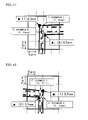
- FIG. 1 is a side view of one example of a printing machine used in the method for producing a screen print according to the present invention.
- FIG. 2 is a top view of one example of screen printing plates used in the method for producing a screen print according to the present invention.
- FIG. 3 is an oblique view showing the state of the screen printing plate being disposed on a printing plate frame holder.
- FIG. 4 is a schematic view showing the points at which the degree of deviation in printing position is measured.
- FIG. 5 is a graph prepared by plotting the results of the measurement of the deviation in the printing position of the initial trial print according to the first selecting and setting method.
- FIG. 6 is an enlarged view of portion A in FIG. 5 .
- FIG. 7 is an enlarged view of portion C in FIG. 5 .
- FIG. 8 is a graph showing one example of plotting a calibration curve and a virtual calibration curve.
- FIG. 9 is a graph showing another example of plotting a calibration curve and a virtual calibration curve.
- FIG. 10 is a graph obtained by plotting the results of measurement of degree of deviation in printing position of the screen print.
- FIG. 11 is an enlarged view of portion A in FIG. 10 .
- FIG. 12 is an enlarged view of portion C in FIG. 10 .
- FIG. 13 is a graph showing one example of plotting a calibration curve according to the second selecting and setting method.
- FIG. 1 is a side view showing one example of a screen printing plate used in the method for producing a screen print according to the present invention
- FIG. 3 is an oblique view showing the state of the screen printing plate being disposed on a printing plate frame holder.
- the screen printing plate 5 is placed on the printing plate frame holder 11 .
- the screen printing plate 5 comprises a filmy screen 3 and a printing plate frame 4 on which the screen 3 is stretched.
- Numeral 6 in FIG. 1 shows an air cylinder which fixes the screen printing plate on the printing plate frame holder 11 .
- FIG. 2 is a top view of one example of the screen printing plates used in the method for producing a screen print according to the present invention.
- screen 3 constituting the screen printing plate 5 has a mask material 2 in which one or more openings 1 having a given opening shape are formed.
- the screen 3 is provided with a filmy supporting member (screen mesh) usually comprising a gauze or the like, and the mask material is disposed on at least one film surface of the screen mesh.
- the material constituting the screen mesh is not particularly limited, but materials of high strength and rigidity are preferred, and as suitable examples, mention may be made of ER wire material and ERH wire material (trademarks) which are screen meshes manufactured by Murakami Co., Ltd.
- the screen printing plate 5 comprises a printing plate frame 4 on which screen 3 is stretched, and the printing plate frame 4 is generally formed of a material having flexibility.
- the general screen printing is carried out at a value of L P /L F of about 0.3.
- the clearance is effectively utilized as a parameter for improving printing precision by employing a value of L P /L F of 0.45 or more.
- a printing material 10 in the form of a flat plate is placed on a printing stage 12 in parallel to the surface of the printing plate frame holder 11 .
- the printing material 10 include those which have been used in conventional screen printing. Suitable printing materials are fired ceramics substrates, ceramics green sheets, resin substrates, glass substrates, metallic substrates, etc.
- the screen printing plate 5 is placed on the printing plate frame holder 11 in such a manner that the printing material 10 (printing surface of the printing material) and the screen 3 are in parallel to each other.
- the screen printing plate 5 is placed keeping a given clearance CL between the printing material 10 and the screen 3 .
- the clearance CL is within the range of 0.1-2 mm, preferably 0.3-1.5 mm, especially preferably 0.4-1.5 mm, especially preferably 0.5-1.3 mm.
- the clearance CL is less than 0.1 mm, defects such as blurring may sometimes occur when the print pattern is formed.
- the clearance CL exceeds 2 mm, elongation of screen 3 caused by sliding of the squeegee is too much, and accordingly, printing of high precision cannot be repeatedly performed.
- the method for producing a screen print according to the present invention is a method which reduces the deviation in the printing position of the print pattern by adjusting the clearance between the printing material and the screen which has not been noticed as a means for improving the positional precision of the print pattern, and thus, according to the present invention it becomes possible to produce a screen print excellent in printing precision.
- the method for producing a screen print of the present invention will be explained in more detail attaching an importance to the method of selecting and setting the optimum clearance.
- Test printing is carried out with setting the clearance at values of optional two or more points in the range of 0.1-2 mm to obtain an initial trial print (step (1)). Then, (2) the degree of deviation in the printing position of the initial trial print is measured, and a calibration curve is prepared by plotting the measured degree of deviation in the printing position against the clearance set above (step (2)).
- FIG. 5 is a graph prepared by plotting the results of measurement of the degree of deviation in printing position of the initial trial print according to the first selecting and setting method.
- FIG. 6 is an enlarged view of portion A in FIG. 5
- FIG. 7 is an enlarged view of portion C in FIG. 5 .
- FIG. 4 schematically shows the points at which the positional precision of the print pattern is measured.
- the clearance is set at every 0.1 mm in the range of 0.3-1.5 mm, and the test printing is conducted at the respective clearances.
- the number of the clearance points set at step (1) may be 2 or more, and to obtain a higher correlation with the degree of deviation in printing position, it is preferred to set the clearances of 3 points or more, and it is even more preferred to set the clearances of 4-5 points. However, setting of clearances of 8 points or more is not preferred because the procedure becomes complicated.
- step (2) as shown in FIG. 8 and FIG. 9 , calibration curves are prepared by plotting the measured degree of deviation in the printing position (mm) against the respective clearances (mm) set above.
- the calibration curves may be prepared by the least-squares method for n-order based on the plotted points.
- FIG. 8 shows the calibration curve ( 1 ) in the case of approximating the cubic function.
- FIG. 9 shows calibration curve ( 2 ) in the case of approximating the linear function.
- step (3) test printing is carried out by setting the clearance at values of the optional one or more points in the range of 0.1-2 mm to obtain a subsequent trial print (step (3)).
- step (3) a screen printing plate which is used which is the same as the screen printing plate used in the design specification step (2), but different individually from the screen printing plate used in step (2) (different individual plates).
- the screen printing plates according to the same design specification show different degrees of deviation in printing position respectively even when the clearance is the same because of individual differences.
- the design specification since the design specification is the same, it can be assumed that the correlation between the clearance and the degree of deviation in printing position are close to each other even in the case of different individual plates.
- the number of clearance points set at step (3) may be 1 point or more. However, the setting of clearances of 3 points or more is not preferred because the procedure becomes complicated.
- step (4) the degree of deviation in printing position of the subsequent trial print is measured, and the measured degree of deviation in the printing position is plotted against the clearance set above, and then the calibration curve is offset to obtain a virtual calibration curve which passes the plotted points (step (4)).
- the measured degree of deviation in the printing position (mm) is plotted against the set clearance (mm).
- FIG. 8 it is shown that two trial prints of the second trail are produced using two screen printing plates while setting the clearance to 0.7 mm.
- the calibration curve ( 1 ) prepared at step (2) is offset in the direction of Y-axis to prepare virtual calibration curves ( 1 ) and ( 2 ) which pass the plotted points (black circle ( ⁇ ) and black triangle ( ⁇ ) in FIG. 8 ).
- the calibration curve can be offset in the directions of X-axis (clearance) and/or Y-axis (degree of deviation in printing position).
- FIG. 9 shows an example in which the calibration curve ( 2 ) expressed by linear function is offset in the direction of Y-axis to prepare a virtual calibration curves ( 3 ) and ( 4 ) which pass the plotted points (black circle ( ⁇ ) and black triangle ( ⁇ ) in FIG. 9 ).
- step (5) the optimum clearance at which the degree of deviation in the printing position of the print pattern is the smallest is selected and set from the virtual calibration curve (step (5)).
- the clearance between the printing material and the screen is set at the optimum clearance read above, and the screen printing is conducted in this state.
- Test printing is carried out with setting the clearance at values of an optional two or more points in the range of 0.1-2 mm to obtain a trial print (step (1a)). Then, in step (2a) the degree of deviation in the printing position of the trial print in step (1a) is measured, and a calibration curve is prepared by plotting the measured degree of deviation in printing position against the clearance set above (step (2a)).
- the number of the points of clearance set at step (6) may be 2 points or more, and for obtaining a higher correlation with the degree of deviation in printing position, it is preferred to set clearances of 3 points or more, and it is even more preferred to set clearances of 4-5 points. However, setting of clearances of 8 points or more is not preferred because the procedure becomes complicated.
- step (2a) the calibration curves are prepared by plotting the measured degree of deviation in the printing position (mm) against the respective clearances (mm) set above.
- the clearance is set at 0.5 mm and 1.0 mm, and the test printing is carried out using three kinds of screen printing plates at the respective clearances to prepare calibration curves ( 3 ), ( 4 ) and ( 5 ).
- the calibration curves may be prepared by the least-squares method for n-order based on the plotted points.
- FIG. 13 shows calibration curves ( 3 ), ( 4 ) and ( 5 ) in the case of approximating the linear function.
- step (3a) the optimum clearance at which the degree of deviation in the printing position of the print pattern is the smallest is selected from the calibration curve and is set (step (3a)).
- selecting and setting of the optimum clearance by the first selecting and setting method is particularly effective when the screen printing plate used for preparation of the calibration curve and the screen printing plate used for actual printing are of the same design specification (lot), but are different individual plates.
- selecting and setting of the optimum clearance by the second selecting and setting method can also be conducted on the condition that the screen printing plate used for preparation of calibration curve and the screen printing plate used for actual printing are the same individual plates.
- the screen printing can be carried out in the following manner. That is, a given ink, paste or the like is put on screen 3 (cf. FIG. 1 ). Then, a squeegee or the like is slid over the screen 3 to squeeze out the paste from the openings, thereby obtaining a screen print comprising the printing material 10 on the printing surface of which is formed a print pattern corresponding to the shape of the opening or corresponding to the arranged pattern of a plurality of the openings that are formed. When the printing is repeatedly carried out on the same printing surface, the printing patterns can be laminated.
- the method for producing a screen print of the present invention use of a parameter as a clearance between a printing material and a screen which has a very high correlation with the degree of deviation in the printing position of the print pattern, the printing can be carried out by selecting an optimum clearance, and hence a printing of very high precision can be obtained. Therefore, a screen print can be produced simply on which a given print pattern of high precision is formed. Furthermore, since a general screen printing plate and a general screen printing machine can be used without any special reconstruction, the method is high in general versatility and a reduction in printing costs can be attained.
- the print pattern is usually required to have a positional precision of about 5 ⁇ m in view of the constraints of the deviation caused by lamination of LTCC substrates.
- the method for producing a screen print of the present invention is particularly effective when the size (internal size) of printing plate frame (screen) is large, namely, 300 mm ⁇ 300 mm ( ⁇ 300 mm, 90000 mm 2 )-400 mm ⁇ 400 mm ( ⁇ 400 mm, 160000 mm 2 ).
- the method is particularly effective when it is a large size of 150 mm ⁇ 150 mm ( ⁇ 150 mm, 22500 mm 2 ) or more, and the size is more preferably 180 mm ⁇ 180 mm ( ⁇ 180 mm, 32400 mm 2 ) or more.
- the screen prints obtained by the method for producing a screen print of the present invention mention may be made of those which have circuits comprising at least dielectrics or conductors that have patterns having passive elements or active elements by virtue of the characteristics that a print screen having a highly precise print pattern may be easily produced.
- the passive elements include capacitor elements, etc. and the active elements include electro-mechanical transducers, etc.
- the screen print is preferably a constituent of laminated substrate obtained by laminating a plurality of the screen prints.
- the laminated substrate are LTCC substrate, ceramic capacitor, laminate type piezoelectric actuator, NO x .oxygen sensor, etc. That is, according to the method for producing a screen print of the present invention, since prints having high precision printing patterns can be produced, when a plurality of the prints are laminated, LTCC substrates having little deviation in print precision from each other caused by lamination can be easily produced. Furthermore, when the resulting LTCC substrates are fired, high performance circuit substrates on which circuits are very precisely disposed can be produced.
- FIG. 4 shows a screen printing plate 5 of 330 mm ⁇ 330 mm in internal size as shown in FIG. 4 (manufactured by Murakami Co., Ltd., the size of the print pattern to be formed: 200 mm ⁇ 200 mm), with a clearance set at every 0.1 mm within the range of 0.3-1.5 mm, with the test printing was conducted with the respective clearances to produce thirteen trial prints according to the first selecting and setting method.
- the degree of deviation in the printing position of the resulting first trial prints (the degree of deviation from the designing center) was measured.
- FIGS. 5-7 show graphs prepared by plotting the results of the measurements.
- the degree of deviation in the printing position (mm) was plotted against the respective clearances (mm) set above to prepare the calibration curves shown in FIG. 8 .
- FIGS. 10-12 show graphs prepared by plotting the results of the measurements.
- the plotted point is shown by black circle ( ⁇ ).
- the measured deviation in the printing position (mm) was plotted against the set clearance (0.7 mm), and the calibration curve prepared hereinbefore was offset in the direction of Y-axis (the degree of deviation in the printing position) to prepare a virtual calibration curve which passed the plotted points.
- FIGS. 10-12 show graphs prepared by plotting the results of the measurements of the degree of deviation in the printing position of the resulting screen prints.
- the point of plotting the results of the measurements of the degree of deviation in the printing position of the second trial print is shown by a black triangle.
- FIG. 13 shows the calibration curves ( 4 ) and ( 5 ) prepared in producing the respective screen prints, and the graphs prepared by plotting the results of the measurements of the degree of deviation in the printing position of the resulting screen prints.
- the method for producing a screen print according to the present invention is suitable as a method for producing various electronic parts since the method can form fine patterns, is high in general versatility, and is suitable for mass-production. Furthermore, according to the method of the present invention, the degree of positional deviation of screen prints can be controlled to a certain range of permissible tolerances. Therefore, the method of the present invention exhibits particularly conspicuous effects in producing laminated electronic parts by laminating a plurality of screen prints.
Landscapes
- Engineering & Computer Science (AREA)
- Manufacturing & Machinery (AREA)
- Microelectronics & Electronic Packaging (AREA)
- Printing Methods (AREA)
- Manufacturing Of Printed Wiring (AREA)
- Screen Printers (AREA)
Abstract
Description
Claims (12)
Applications Claiming Priority (4)
| Application Number | Priority Date | Filing Date | Title |
|---|---|---|---|
| JP2007061968 | 2007-03-12 | ||
| JP2007-061968 | 2007-03-12 | ||
| JP2007282973A JP5011065B2 (en) | 2007-03-12 | 2007-10-31 | Method for producing screen printing body |
| JP2007-282973 | 2007-10-31 |
Publications (2)
| Publication Number | Publication Date |
|---|---|
| US20080223234A1 US20080223234A1 (en) | 2008-09-18 |
| US7730833B2 true US7730833B2 (en) | 2010-06-08 |
Family
ID=39761341
Family Applications (1)
| Application Number | Title | Priority Date | Filing Date |
|---|---|---|---|
| US11/970,795 Expired - Fee Related US7730833B2 (en) | 2007-03-12 | 2008-01-08 | Method for producing screen print by selecting clearance between screen and printing material |
Country Status (1)
| Country | Link |
|---|---|
| US (1) | US7730833B2 (en) |
Families Citing this family (2)
| Publication number | Priority date | Publication date | Assignee | Title |
|---|---|---|---|---|
| TW201313489A (en) * | 2011-09-16 | 2013-04-01 | Askey Technology Jiangsu Ltd | Stencil for coating solder paste on printed circuit board |
| CN112389077B (en) * | 2020-11-18 | 2022-05-31 | 昆明原伯腾印刷有限公司 | High-precision screen printing equipment |
Citations (5)
| Publication number | Priority date | Publication date | Assignee | Title |
|---|---|---|---|---|
| JPH09136394A (en) | 1995-11-14 | 1997-05-27 | Ise Electronics Corp | Plate for screen printing |
| JPH1134288A (en) | 1997-07-17 | 1999-02-09 | Ngk Insulators Ltd | Plate making process for screen printing |
| JP2000318120A (en) | 1999-05-10 | 2000-11-21 | Noritake Co Ltd | Screen printing method |
| JP2006062241A (en) | 2004-08-27 | 2006-03-09 | Ngk Insulators Ltd | Plate for screen printing and manufacturing method of printing body using the same |
| US20080098911A1 (en) * | 2006-10-31 | 2008-05-01 | Fujitsu Hitachi Plasma Display Limited | Screen mask |
-
2008
- 2008-01-08 US US11/970,795 patent/US7730833B2/en not_active Expired - Fee Related
Patent Citations (5)
| Publication number | Priority date | Publication date | Assignee | Title |
|---|---|---|---|---|
| JPH09136394A (en) | 1995-11-14 | 1997-05-27 | Ise Electronics Corp | Plate for screen printing |
| JPH1134288A (en) | 1997-07-17 | 1999-02-09 | Ngk Insulators Ltd | Plate making process for screen printing |
| JP2000318120A (en) | 1999-05-10 | 2000-11-21 | Noritake Co Ltd | Screen printing method |
| JP2006062241A (en) | 2004-08-27 | 2006-03-09 | Ngk Insulators Ltd | Plate for screen printing and manufacturing method of printing body using the same |
| US20080098911A1 (en) * | 2006-10-31 | 2008-05-01 | Fujitsu Hitachi Plasma Display Limited | Screen mask |
Also Published As
| Publication number | Publication date |
|---|---|
| US20080223234A1 (en) | 2008-09-18 |
Similar Documents
| Publication | Publication Date | Title |
|---|---|---|
| KR100843183B1 (en) | Screen mask | |
| US20080196608A1 (en) | Screen Printing Plate and Screen Printing Apparatus | |
| US20140174309A1 (en) | Method of Screen Printing on Low Temperature Co-Fired Ceramic (LTCC) Tape | |
| CN115972748B (en) | Screen | |
| US7730833B2 (en) | Method for producing screen print by selecting clearance between screen and printing material | |
| KR20120032247A (en) | Method for revision of printing error in pcb | |
| US6794582B2 (en) | Mask for screen printing, the method for producing same and circuit board produced by screen printing with such mask | |
| JP2023138827A (en) | Screen mask, screen mask manufacturing method, and printed matter manufacturing method | |
| JP5009631B2 (en) | Method for producing screen printing body | |
| JPH0585077A (en) | Screen printing plate and production thereof | |
| CN214727284U (en) | Bearing piece for screen printing and screen printing screen | |
| JP5011065B2 (en) | Method for producing screen printing body | |
| JP2006062241A (en) | Plate for screen printing and manufacturing method of printing body using the same | |
| JP5331448B2 (en) | Method for producing screen printing body | |
| CN112848723A (en) | Printing process for improving brightness uniformity and picture effect of glass diffusion plate | |
| JP5697830B2 (en) | Screen printing plate and screen printing device | |
| CN100553971C (en) | Method and apparatus for printing a patterned layer on a flat substrate using a flat bed machine | |
| JP7112123B2 (en) | SCREEN MASK AND PRINTED MATERIAL MANUFACTURING METHOD | |
| JPH10315647A (en) | Screen printing plate | |
| JP5726841B2 (en) | Substrate printing device | |
| CN111942045A (en) | Overprinting method for accurately coating reflective white oil on Mini-LED | |
| JP2007062225A (en) | Combination screen plate and combination metal mask plate | |
| KR20190019533A (en) | Gravure offset roll for printing electronic with fine pattern and manufacturing method | |
| JPH11245373A (en) | Screen printing plate | |
| JP2008229898A (en) | Screen plate and electronic part manufacturing method |
Legal Events
| Date | Code | Title | Description |
|---|---|---|---|
| AS | Assignment |
Owner name: NGK INSULATORS, LTD., JAPAN Free format text: ASSIGNMENT OF ASSIGNORS INTEREST;ASSIGNORS:OHMORI, MAKOTO;AISAKA, YUKIO;IDA, AYUMI;AND OTHERS;REEL/FRAME:020333/0252 Effective date: 20071224 Owner name: NGK INSULATORS, LTD.,JAPAN Free format text: ASSIGNMENT OF ASSIGNORS INTEREST;ASSIGNORS:OHMORI, MAKOTO;AISAKA, YUKIO;IDA, AYUMI;AND OTHERS;REEL/FRAME:020333/0252 Effective date: 20071224 |
|
| STCF | Information on status: patent grant |
Free format text: PATENTED CASE |
|
| FEPP | Fee payment procedure |
Free format text: PAYOR NUMBER ASSIGNED (ORIGINAL EVENT CODE: ASPN); ENTITY STATUS OF PATENT OWNER: LARGE ENTITY |
|
| FPAY | Fee payment |
Year of fee payment: 4 |
|
| MAFP | Maintenance fee payment |
Free format text: PAYMENT OF MAINTENANCE FEE, 8TH YEAR, LARGE ENTITY (ORIGINAL EVENT CODE: M1552) Year of fee payment: 8 |
|
| FEPP | Fee payment procedure |
Free format text: MAINTENANCE FEE REMINDER MAILED (ORIGINAL EVENT CODE: REM.); ENTITY STATUS OF PATENT OWNER: LARGE ENTITY |
|
| LAPS | Lapse for failure to pay maintenance fees |
Free format text: PATENT EXPIRED FOR FAILURE TO PAY MAINTENANCE FEES (ORIGINAL EVENT CODE: EXP.); ENTITY STATUS OF PATENT OWNER: LARGE ENTITY |
|
| STCH | Information on status: patent discontinuation |
Free format text: PATENT EXPIRED DUE TO NONPAYMENT OF MAINTENANCE FEES UNDER 37 CFR 1.362 |
|
| FP | Lapsed due to failure to pay maintenance fee |
Effective date: 20220608 |