US7727825B2 - Polyconductor line end formation and related mask - Google Patents

Polyconductor line end formation and related mask Download PDF

Info

Publication number
US7727825B2
US7727825B2 US12/178,072 US17807208A US7727825B2 US 7727825 B2 US7727825 B2 US 7727825B2 US 17807208 A US17807208 A US 17807208A US 7727825 B2 US7727825 B2 US 7727825B2
Authority
US
United States
Prior art keywords
polyconductor
mask
line ends
correction element
shape
Prior art date
Legal status (The legal status is an assumption and is not a legal conclusion. Google has not performed a legal analysis and makes no representation as to the accuracy of the status listed.)
Expired - Fee Related
Application number
US12/178,072
Other versions
US20090117737A1 (en
Inventor
Shahid A. Butt
Allen H. Gabor
Donald J. Samuels
Current Assignee (The listed assignees may be inaccurate. Google has not performed a legal analysis and makes no representation or warranty as to the accuracy of the list.)
Alsephina Innovations Inc
Original Assignee
International Business Machines Corp
Priority date (The priority date is an assumption and is not a legal conclusion. Google has not performed a legal analysis and makes no representation as to the accuracy of the date listed.)
Filing date
Publication date
Application filed by International Business Machines Corp filed Critical International Business Machines Corp
Priority to US12/178,072 priority Critical patent/US7727825B2/en
Publication of US20090117737A1 publication Critical patent/US20090117737A1/en
Application granted granted Critical
Publication of US7727825B2 publication Critical patent/US7727825B2/en
Assigned to GLOBALFOUNDRIES U.S. 2 LLC reassignment GLOBALFOUNDRIES U.S. 2 LLC ASSIGNMENT OF ASSIGNORS INTEREST (SEE DOCUMENT FOR DETAILS). Assignors: INTERNATIONAL BUSINESS MACHINES CORPORATION
Assigned to GLOBALFOUNDRIES INC. reassignment GLOBALFOUNDRIES INC. ASSIGNMENT OF ASSIGNORS INTEREST (SEE DOCUMENT FOR DETAILS). Assignors: GLOBALFOUNDRIES U.S. 2 LLC, GLOBALFOUNDRIES U.S. INC.
Assigned to ALSEPHINA INNOVATIONS INC. reassignment ALSEPHINA INNOVATIONS INC. ASSIGNMENT OF ASSIGNORS INTEREST (SEE DOCUMENT FOR DETAILS). Assignors: GLOBALFOUNDRIES INC.
Expired - Fee Related legal-status Critical Current
Anticipated expiration legal-status Critical

Links

Images

Classifications

    • GPHYSICS
    • G03PHOTOGRAPHY; CINEMATOGRAPHY; ANALOGOUS TECHNIQUES USING WAVES OTHER THAN OPTICAL WAVES; ELECTROGRAPHY; HOLOGRAPHY
    • G03FPHOTOMECHANICAL PRODUCTION OF TEXTURED OR PATTERNED SURFACES, e.g. FOR PRINTING, FOR PROCESSING OF SEMICONDUCTOR DEVICES; MATERIALS THEREFOR; ORIGINALS THEREFOR; APPARATUS SPECIALLY ADAPTED THEREFOR
    • G03F7/00Photomechanical, e.g. photolithographic, production of textured or patterned surfaces, e.g. printing surfaces; Materials therefor, e.g. comprising photoresists; Apparatus specially adapted therefor
    • G03F7/70Microphotolithographic exposure; Apparatus therefor
    • G03F7/70425Imaging strategies, e.g. for increasing throughput or resolution, printing product fields larger than the image field or compensating lithography- or non-lithography errors, e.g. proximity correction, mix-and-match, stitching or double patterning
    • G03F7/70433Layout for increasing efficiency or for compensating imaging errors, e.g. layout of exposure fields for reducing focus errors; Use of mask features for increasing efficiency or for compensating imaging errors
    • G03F7/70441Optical proximity correction [OPC]
    • GPHYSICS
    • G03PHOTOGRAPHY; CINEMATOGRAPHY; ANALOGOUS TECHNIQUES USING WAVES OTHER THAN OPTICAL WAVES; ELECTROGRAPHY; HOLOGRAPHY
    • G03FPHOTOMECHANICAL PRODUCTION OF TEXTURED OR PATTERNED SURFACES, e.g. FOR PRINTING, FOR PROCESSING OF SEMICONDUCTOR DEVICES; MATERIALS THEREFOR; ORIGINALS THEREFOR; APPARATUS SPECIALLY ADAPTED THEREFOR
    • G03F1/00Originals for photomechanical production of textured or patterned surfaces, e.g., masks, photo-masks, reticles; Mask blanks or pellicles therefor; Containers specially adapted therefor; Preparation thereof
    • G03F1/36Masks having proximity correction features; Preparation thereof, e.g. optical proximity correction [OPC] design processes
    • HELECTRICITY
    • H01ELECTRIC ELEMENTS
    • H01LSEMICONDUCTOR DEVICES NOT COVERED BY CLASS H10
    • H01L21/00Processes or apparatus adapted for the manufacture or treatment of semiconductor or solid state devices or of parts thereof
    • H01L21/02Manufacture or treatment of semiconductor devices or of parts thereof
    • H01L21/027Making masks on semiconductor bodies for further photolithographic processing not provided for in group H01L21/18 or H01L21/34
    • H01L21/033Making masks on semiconductor bodies for further photolithographic processing not provided for in group H01L21/18 or H01L21/34 comprising inorganic layers
    • H01L21/0334Making masks on semiconductor bodies for further photolithographic processing not provided for in group H01L21/18 or H01L21/34 comprising inorganic layers characterised by their size, orientation, disposition, behaviour, shape, in horizontal or vertical plane
    • H01L21/0335Making masks on semiconductor bodies for further photolithographic processing not provided for in group H01L21/18 or H01L21/34 comprising inorganic layers characterised by their size, orientation, disposition, behaviour, shape, in horizontal or vertical plane characterised by their behaviour during the process, e.g. soluble masks, redeposited masks
    • HELECTRICITY
    • H01ELECTRIC ELEMENTS
    • H01LSEMICONDUCTOR DEVICES NOT COVERED BY CLASS H10
    • H01L21/00Processes or apparatus adapted for the manufacture or treatment of semiconductor or solid state devices or of parts thereof
    • H01L21/02Manufacture or treatment of semiconductor devices or of parts thereof
    • H01L21/04Manufacture or treatment of semiconductor devices or of parts thereof the devices having at least one potential-jump barrier or surface barrier, e.g. PN junction, depletion layer or carrier concentration layer
    • H01L21/18Manufacture or treatment of semiconductor devices or of parts thereof the devices having at least one potential-jump barrier or surface barrier, e.g. PN junction, depletion layer or carrier concentration layer the devices having semiconductor bodies comprising elements of Group IV of the Periodic System or AIIIBV compounds with or without impurities, e.g. doping materials
    • H01L21/30Treatment of semiconductor bodies using processes or apparatus not provided for in groups H01L21/20 - H01L21/26
    • H01L21/31Treatment of semiconductor bodies using processes or apparatus not provided for in groups H01L21/20 - H01L21/26 to form insulating layers thereon, e.g. for masking or by using photolithographic techniques; After treatment of these layers; Selection of materials for these layers
    • H01L21/3205Deposition of non-insulating-, e.g. conductive- or resistive-, layers on insulating layers; After-treatment of these layers
    • H01L21/321After treatment
    • H01L21/3213Physical or chemical etching of the layers, e.g. to produce a patterned layer from a pre-deposited extensive layer
    • H01L21/32139Physical or chemical etching of the layers, e.g. to produce a patterned layer from a pre-deposited extensive layer using masks
    • HELECTRICITY
    • H01ELECTRIC ELEMENTS
    • H01LSEMICONDUCTOR DEVICES NOT COVERED BY CLASS H10
    • H01L21/00Processes or apparatus adapted for the manufacture or treatment of semiconductor or solid state devices or of parts thereof
    • H01L21/70Manufacture or treatment of devices consisting of a plurality of solid state components formed in or on a common substrate or of parts thereof; Manufacture of integrated circuit devices or of parts thereof
    • H01L21/71Manufacture of specific parts of devices defined in group H01L21/70
    • H01L21/768Applying interconnections to be used for carrying current between separate components within a device comprising conductors and dielectrics
    • H01L21/76838Applying interconnections to be used for carrying current between separate components within a device comprising conductors and dielectrics characterised by the formation and the after-treatment of the conductors

Abstract

Methods of forming adjacent polyconductor line ends and a mask therefor are disclosed. In one embodiment, the method includes forming a polyconductor layer over an isolation region; forming a mask over the polyconductor layer, the mask including shapes to create the polyconductor line ends and a correction element to ensure a designed proximity of the polyconductor line ends; and etching the polyconductor layer using the patterned photoresist mask to create the adjacent polyconductor line ends, wherein the correction element is removed during the etching.

Description

REFERENCE TO PRIOR APPLICATIONS
This application is a continuation application of U.S. patent application Ser. No. 11/935,714 filed on Nov. 6, 2007 now U.S. Pat. No. 7,465,615, which is hereby incorporated by reference.
BACKGROUND
1. Technical Field
The disclosure relates generally to integrated circuit (IC) chip fabrication, and more particularly, to methods of forming polyconductor line ends and a memory cell including the polyconductor line ends.
2. Background Art
Memory used in integrated circuit (IC) chips can come in a variety of forms such as static random access memory (SRAM), dynamic random access memory (DRAM), Flash memory, etc. The industry has a continuing drive to shrink memory cells to remain competitive. As one attempts to shrink cells, process constraints can limit the amount of shrinkage. As isolation regions (e.g., shallow trench isolation (STI)) push closer together, the distance that a polysilicon conductor (polyconductor or PC) can extend pass the STI is decreased. The cell dimension is limited by how close one can place to PC lines end-to-end (facing each other or otherwise) on the isolation region. Thus, the performance of a memory cell is directly influenced by the end-to-end space that can be achieved between PC line-ends.
The ability to pattern a small space between PC line-ends has both lithographic and etch limitations. The etch limitations come from the fact that during the trim step (i.e., the process in which the gate critical dimension (CD) that was printed in photoresist is reduced to that which is needed in the final poly) the line-ends trim more than the gates. In particular, as shown in FIG. 1, a specific PC line-end 2 may be targeted to be, for example, 100 nm, past an active region 4 (scenario A) or contact layer 6 (scenario B) into an isolation region 8, but due to limitations of the resist, trim processing and rounding, PC line-end 2 does not end up being 100 nm past the active region 6 or contact layer 8. In some instances, PC line-end 2 is etched back over active region 4. In any event, it is common for a gate length to be incorrect because of this situation. Further scaling magnifies the situation.
There are many methods which are being pursued in the industry to enable the tighter PC line-end spacing. For example, one popular approach includes a double exposure-double etch scheme. In this case, as shown in FIG. 2A, a polyconductor (PC) 12 is exposed and etched over an active region 14 and fully across an isolation region 16 to print a gate 18 (intersection of PC 12 and active region 14), and then another exposure and etch, shown in FIG. 2B, is used to remove polyconductor 12 over the isolation region 16 to form line-ends 22 and, hence, the devices. This approach attains the necessary sizes and precision, however, the cost incurred is significant because of the need for two exposures and two etches for one level. It allows the etch step for opening line-ends 22 to be completely directional (no trim) and also creates PC tips that are relatively less rounded. The rounded line ends trim very quickly during the etch process, which makes controlling the etch difficult.
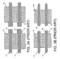
A second approach, shown in FIGS. 3A-B, attempts to decrease the trim rate of line-ends 22 (FIG. 2B) by printing a bulged region 24 (FIG. 3A) in the resist at a line-end for polyconductor 12 (single exposure, single etch) over isolation region 16. That is, line ends 22 (FIG. 2B) are printed in the resist with bulged region 24 immediately adjacent to active region 14. This approach offers smaller spacing due to the decreased trim of the line-ends, but creates bulbous line-ends 26 (FIG. 3B). Unfortunately, bulbous line-ends 26 usually land on active region 14, which causes undesirable gate 18 length variation along the device. A third approach includes using a double exposure with a single etch. While this approach does not eliminate the etch effects, it allows for a smaller line-end space to be printed in resist if the illumination is optimized for the second exposure. A fourth approach under exposes the PC using a block mask, and uses alternating phase shift masks (Alt PSM) scheme and a break through with etch.
SUMMARY
Methods of forming adjacent polyconductor line ends and a mask therefor are disclosed. In one embodiment, the method includes forming a polyconductor layer over an isolation region; forming a mask over the polyconductor layer, the mask including a shape to create each polyconductor line end and a correction element to ensure a designed proximity of the polyconductor line ends; and etching the polyconductor layer using the patterned photoresist mask to create the adjacent polyconductor line ends, wherein the correction element is removed during the etching.
A first aspect of the disclosure provides a method of forming adjacent polyconductor line ends, the method comprising: forming a polyconductor layer over an isolation region; forming a mask over the polyconductor layer, the mask including a shape to create the polyconductor line ends and a correction element to ensure a designed proximity of the polyconductor line ends; and etching the polyconductor layer using the patterned photoresist mask to create the adjacent polyconductor line ends, wherein the correction element is removed during the etching.
A second aspect of the disclosure provides a mask for forming adjacent polyconductor line ends, the mask comprising: a shape to create each polyconductor line end; and a correction element having a dimension such that the correction element does not print during use of the mask but ensures a designed line end proximity of the polyconductor line ends.
A third aspect of the disclosure provides a method of forming adjacent polyconductor line ends, the method comprising: forming a polyconductor layer over an isolation region; forming a mask over the polyconductor layer, the mask including a shape to create each polyconductor line end and a sub-resolution correction element to ensure a designed proximity of the polyconductor line ends, wherein the sub-resolution correction element exists despite any optical correction; and etching the polyconductor layer using the patterned photoresist mask to create the adjacent polyconductor line ends, wherein the correction element is removed during the etching.
The illustrative aspects of the present disclosure are designed to solve the problems herein described and/or other problems not discussed.
BRIEF DESCRIPTION OF THE DRAWINGS
These and other features of this disclosure will be more readily understood from the following detailed description of the various aspects of the disclosure taken in conjunction with the accompanying drawings that depict various embodiments of the disclosure, in which:
FIG. 1 shows a simplified conventional memory cell.
FIGS. 2A-B shows a simplified method of forming polyconductor line ends for a memory cell.
FIGS. 3A-B shows another simplified method of forming polyconductor line ends for a memory cell.
FIG. 4 shows one embodiment of a polyconductor line ends according to an intended design.
FIG. 5 shows one process according to embodiments of a method according to the disclosure.
FIGS. 6-10 show other processes of the embodiments of the method and various embodiments of a mask according to the disclosure.
It is noted that the drawings of the disclosure are not to scale. The drawings are intended to depict only typical aspects of the disclosure, and therefore should not be considered as limiting the scope of the disclosure. In the drawings, like numbering represents like elements between the drawings.
DETAILED DESCRIPTION
Referring to FIGS. 4-10, embodiments of a method of forming adjacent polyconductor line ends 100A-B and a related mask 102 (FIG. 6) are illustrated. The methods and mask 102 take advantage of the large, non-linear etch biases experienced by polyconductor line etching by forming a correction element 160 (FIGS. 6-10)(during lithography) between adjacent polyconductor line ends 100A, 100B that has a size that is less than an etch bias, i.e., {DEFINE ETCH BIAS} sub-resolution. As a result, after etching, the correction element is removed or broken and two adjacent polyconductor line ends 100A, 100B are created with less line end shortening than with a conventional single expose process. Correction elements 160 will be made by introducing sub-resolution features in the gap between polyconductor line ends 100A, 100B, e.g., over an isolation region 116. Since polyconductor line ends 100A-B are so close, what would normally be sub resolution, in fact will print. The embodiments illustrated pertain to forming a memory cell, e.g., static random access memory (SRAM) cell, dynamic random access memory (DRAM) cell, Flash memory, etc. It is understood, however, that the teachings of the disclosure are not limited to formation of a memory cell, and may find applicability to a variety of situations requiring decreased spacing between polyconductor line ends. It is emphasized here that the teachings of the disclosure are apart from optical correction, which may also be provided.
FIG. 4 shows one embodiment of polyconductor lines 100A-B over device elements 114A, 114B separated by an isolation region 116. More particularly, FIG. 4 shows polyconductor lines 100A-B as they were designed to be formed, e.g., at a certain distance apart, having square ends, etc. As used herein, a “device element” may include any structure over which a polyconductor line is to extend. In one embodiment, each device element 114A, 114B includes an active region, i.e., a doped silicon region over which a polyconductor line 112A, 112B (two shown) forms a gate 118. In another embodiment, one device element 114A may include an active region, while device element 114B includes a contact element, e.g., a contact via or contact level interconnect (similar to contact layer 6 in FIG. 1). Other device elements may also be possible. Isolation region 116 may include any now known or later developed isolation structure, e.g., a deep trench isolation, a shallow trench isolation, etc., and may include any appropriate dielectric such as silicon dioxide (SiO2). Device elements 114A, 114B and isolation region 116 may be formed using any now known or later develop processes, e.g., silicon deposition, trench formation using photolithography, dielectric deposition, planarization, etc.
FIG. 5 shows a first process including forming a polyconductor layer 140 over isolation region 116. FIG. 5 also shows a photoresist layer 150 over polyconductor layer 140. (Both polyconductor layer 140 and photoresist layer 150 are shown in a transparent manner so that underlying structures are apparent). Polyconductor layer 140 may include any now known or later developed polycrystalline silicon conductor material, doped or undoped.
FIG. 5 also shows forming mask 102 (FIG. 6) over polyconductor layer 140. This process may include any now known or later developed techniques for generally creating a mask 102. In the example shown, a hardmask 152 is formed (patterned) over photoresist 150, and the photoresist is etched to form mask 102. Mask 102 is used to etch polyconductor layer 140. FIG. 5 shows only one embodiment of shapes used in mask 102 in FIG. 6. It is understood, however, that other hardmask 152 shapes may be used to form other mask 102 shapes such as those shown in FIGS. 7-10.
With reference to FIG. 4 and FIGS. 6-10, mask 102 includes a shape 150A, 150B to, among other things, create a polyconductor line ends 100A, 100B and a correction element 160 to ensure a designed line end proximity of polyconductor line ends 100A, 100B. Correction element 160 is a sub-resolution feature and may be introduced during conventional optical proximity correction (OPC) processing flow. OPC is a process that attempts to normalize images on a mask to attain desired space to accommodate the diffraction problems caused by shapes printing smaller than the wavelength of light used for photolithography. Correction element 160 exists despite any optical proximity correction, i.e., it is not created as part of or removed by OPC. As shown in FIG. 4, OPC should give: a) a square end to line ends 100A, 100B, and b) lines ends 100A, 100B that extend past device elements 114A, 114B, because that is what a designer intended. In reality, neighboring shapes present constraints as to how far OPC can move shapes, so polyconductor line ends 100A, 100B end up too short and not square. Correction element 160 provides OPC processing a target to force line ends 100A, 100B to bridge, and exists despite OPC. Correction element 160 can either be put in before OPC and OPC is allowed to see the feature, or correction element 160 can be put in either before or after OPC, but OPC is not allowed to see the feature.
Each of FIGS. 6-10 shows an embodiment of correction element 160. Note that in FIGS. 6-10, correction element 160 includes a border for clarity of illustration purposes only. In the FIG. 6 embodiment, correction element 160 includes a bridge element 170 spanning an opening 172 between each shape 150A, 150B of mask 102 for polyconductor line ends 100A, 100B. FIG. 7 shows correction element 160 including an island 174 positioned in opening 172 between each shape 150A, 150B of mask 102 for polyconductor line ends 100A, 100B. FIG. 8 shows correction element 160 including an element 176 extending substantially perpendicularly to each shape 150A, 150B of mask 102 for polyconductor line ends 100A, 100B in opening 172 between each shape 150A, 150B of mask 102 for the polyconductor line ends 100A, 100B. FIG. 9 shows correction element 160 including a first element 180 positioned to a first side 182 of opening 172 between each shape 150A, 150B of mask 102 for polyconductor line ends 100A, 100B and laterally overlapping each shape 150A, 150B, and a second element 186 positioned to a second side 188 of opening 172 and laterally overlapping shapes 150A, 150B. FIG. 10 shows an alternative embodiment that shown in FIG. 6. In this embodiment, correction element 160 includes bridge element 170 spanning opening 172 between each shape 150A, 150B of mask 102 for polyconductor line ends 100A, 100B, and each shape 150A, 150B includes a void 190. Voids 190 extend to polyconductor layer 140.
In either embodiment, mask 102 for forming adjacent polyconductor line ends 100A, 100B includes a shape 150A, 150B to create each polyconductor line end 100A, 100B, and correction element 160 having a dimension such that the correction element does not print during use of the mask but ensures a designed line end proximity of the polyconductor line ends.
Etching of polyconductor layer 140 using patterned photoresist mask 102 creates the adjacent polyconductor line ends 100A, 100B, as shown in FIG. 4. As also shown in FIG. 4, correction element 160 is removed during the etching. The etching may use any now known or later developed etching process such as reactive ion etching (RIE).
The methods and mask as described above are used in the fabrication of integrated circuit chips. The resulting integrated circuit chips can be distributed by the fabricator in raw wafer form (that is, as a single wafer that has multiple unpackaged chips), as a bare die, or in a packaged form. In the latter case the chip is mounted in a single chip package (such as a plastic carrier, with leads that are affixed to a motherboard or other higher level carrier) or in a multichip package (such as a ceramic carrier that has either or both surface interconnections or buried interconnections). In any case the chip is then integrated with other chips, discrete circuit elements, and/or other signal processing devices as part of either (a) an intermediate product, such as a motherboard, or (b) an end product. The end product can be any product that includes integrated circuit chips, ranging from toys and other low-end applications to advanced computer products having a display, a keyboard or other input device, and a central processor.
The foregoing description of various aspects of the disclosure has been presented for purposes of illustration and description. It is not intended to be exhaustive or to limit the disclosure to the precise form disclosed, and obviously, many modifications and variations are possible. Such modifications and variations that may be apparent to a person skilled in the art are intended to be included within the scope of the disclosure as defined by the accompanying claims.

Claims (15)

1. A method of forming adjacent polyconductor line ends, the method comprising:
forming a polyconductor layer over an isolation region;
forming a mask over the polyconductor layer, the mask including a shape to create the polyconductor line ends and a correction element to ensure a designed proximity of the polyconductor line ends; and
etching the polyconductor layer using the patterned photoresist mask to create the adjacent polyconductor line ends, wherein the correction element is removed during the etching.
2. The method of claim 1, wherein the correction element includes a bridge element spanning an opening between each shape of the mask for the polyconductor line ends.
3. The method of claim 1, wherein the correction element includes an island positioned in an opening between each shape of the mask for the polyconductor line ends.
4. The method of claim 1, wherein the correction element includes an element extending substantially perpendicularly to each shape of the mask for the polyconductor line ends in an opening between each shape of the mask for the polyconductor line ends.
5. The method of claim 1, wherein the correction element includes a first element positioned to a first side of an opening between each shape of the mask for the polyconductor line ends and laterally overlapping the shapes, and a second element positioned to a second side of the opening and laterally overlapping the shapes.
6. The method of claim 1, wherein the correction element has a dimension that is sub-resolution.
7. The method of claim 1, wherein the correction element exists despite any optical proximity correction (OPC).
8. The method of claim 2, wherein the mask forming includes forming a void in each shape of the mask for the polyconductor line ends.
9. A mask for forming adjacent polyconductor line ends, the mask comprising:
a shape to create each polyconductor line end;
a correction element having a dimension such that the correction element does not print during use of the mask but ensures a designed line end proximity of the polyconductor line ends, wherein the correction element includes a bridge element spanning an opening between each shape of the mask for the polyconductor line ends; and
a void in each shape of the mask for the polyconductor line ends.
10. A method of forming adjacent polyconductor line ends, the method comprising:
forming a polyconductor layer over an isolation region;
forming a mask over the polyconductor layer, the mask including a shape to create each polyconductor line end and a sub-resolution correction element to ensure a designed proximity of the polyconductor line ends, wherein the sub-resolution correction element exists despite any optical correction; and
etching the polyconductor layer using the patterned photoresist mask to create the adjacent polyconductor line ends, wherein the correction element is removed during the etching.
11. The method of claim 10, wherein the correction element includes a bridge element spanning an opening between each shape of the mask for the polyconductor line ends.
12. The method of claim 10, wherein the correction element includes an island positioned in an opening between each shape of the mask for the polyconductor line ends.
13. The method of claim 10, wherein the correction element includes an element extending substantially perpendicularly to each shape of the mask for the polyconductor line ends in an opening between the shapes.
14. The method of claim 10, wherein the correction element includes a first element positioned to a first side of an opening between each shape of the mask for the polyconductor line ends and laterally overlapping the shapes, and a second element positioned to a second side of the opening and laterally overlapping the shapes.
15. The method of claim 11, wherein the mask forming includes forming a void in each shape of the mask for the polyconductor line ends of the mask.
US12/178,072 2007-11-06 2008-07-23 Polyconductor line end formation and related mask Expired - Fee Related US7727825B2 (en)

Priority Applications (1)

Application Number Priority Date Filing Date Title
US12/178,072 US7727825B2 (en) 2007-11-06 2008-07-23 Polyconductor line end formation and related mask

Applications Claiming Priority (2)

Application Number Priority Date Filing Date Title
US11/935,714 US7465615B1 (en) 2007-11-06 2007-11-06 Polyconductor line end formation and related mask
US12/178,072 US7727825B2 (en) 2007-11-06 2008-07-23 Polyconductor line end formation and related mask

Related Parent Applications (1)

Application Number Title Priority Date Filing Date
US11/935,714 Continuation US7465615B1 (en) 2007-11-06 2007-11-06 Polyconductor line end formation and related mask

Publications (2)

Publication Number Publication Date
US20090117737A1 US20090117737A1 (en) 2009-05-07
US7727825B2 true US7727825B2 (en) 2010-06-01

Family

ID=40118686

Family Applications (2)

Application Number Title Priority Date Filing Date
US11/935,714 Active US7465615B1 (en) 2007-11-06 2007-11-06 Polyconductor line end formation and related mask
US12/178,072 Expired - Fee Related US7727825B2 (en) 2007-11-06 2008-07-23 Polyconductor line end formation and related mask

Family Applications Before (1)

Application Number Title Priority Date Filing Date
US11/935,714 Active US7465615B1 (en) 2007-11-06 2007-11-06 Polyconductor line end formation and related mask

Country Status (1)

Country Link
US (2) US7465615B1 (en)

Cited By (1)

* Cited by examiner, † Cited by third party
Publication number Priority date Publication date Assignee Title
US20100117187A1 (en) * 2008-11-07 2010-05-13 Dae-Kyeun Kim Method for forming gate in fabricating semiconductor device

Families Citing this family (3)

* Cited by examiner, † Cited by third party
Publication number Priority date Publication date Assignee Title
US7465615B1 (en) * 2007-11-06 2008-12-16 International Business Machines Corporation Polyconductor line end formation and related mask
US9087739B2 (en) * 2009-10-19 2015-07-21 International Business Machines Corporation Pattern improvement in multiprocess patterning
US10417369B2 (en) * 2017-05-26 2019-09-17 Taiwan Semiconductor Manufacturing Company, Ltd. Semiconductor device, corresponding mask and method for generating layout of same

Citations (7)

* Cited by examiner, † Cited by third party
Publication number Priority date Publication date Assignee Title
US4343877A (en) 1981-01-02 1982-08-10 Amdahl Corporation System for design and production of integrated circuit photomasks and integrated circuit devices
US6034877A (en) 1998-06-08 2000-03-07 International Business Machines Corporation Semiconductor memory array having sublithographic spacing between adjacement trenches and method for making the same
US6430733B1 (en) 1999-04-22 2002-08-06 International Business Machines Corporation Contextual based groundrule compensation method of mask data set generation
US6593631B2 (en) 1997-03-13 2003-07-15 Hynix Semiconductor Inc. Method of fabricating semiconductor device
US20050271949A1 (en) 2002-12-09 2005-12-08 Scott Corboy Reticle manipulations
US20070128526A1 (en) * 2005-12-07 2007-06-07 Intel Corporation Non-collinear end-to-end structures with sub-resolution assist features
US7465615B1 (en) * 2007-11-06 2008-12-16 International Business Machines Corporation Polyconductor line end formation and related mask

Patent Citations (7)

* Cited by examiner, † Cited by third party
Publication number Priority date Publication date Assignee Title
US4343877A (en) 1981-01-02 1982-08-10 Amdahl Corporation System for design and production of integrated circuit photomasks and integrated circuit devices
US6593631B2 (en) 1997-03-13 2003-07-15 Hynix Semiconductor Inc. Method of fabricating semiconductor device
US6034877A (en) 1998-06-08 2000-03-07 International Business Machines Corporation Semiconductor memory array having sublithographic spacing between adjacement trenches and method for making the same
US6430733B1 (en) 1999-04-22 2002-08-06 International Business Machines Corporation Contextual based groundrule compensation method of mask data set generation
US20050271949A1 (en) 2002-12-09 2005-12-08 Scott Corboy Reticle manipulations
US20070128526A1 (en) * 2005-12-07 2007-06-07 Intel Corporation Non-collinear end-to-end structures with sub-resolution assist features
US7465615B1 (en) * 2007-11-06 2008-12-16 International Business Machines Corporation Polyconductor line end formation and related mask

Cited By (1)

* Cited by examiner, † Cited by third party
Publication number Priority date Publication date Assignee Title
US20100117187A1 (en) * 2008-11-07 2010-05-13 Dae-Kyeun Kim Method for forming gate in fabricating semiconductor device

Also Published As

Publication number Publication date
US20090117737A1 (en) 2009-05-07
US7465615B1 (en) 2008-12-16

Similar Documents

Publication Publication Date Title
US7776750B2 (en) Semiconductor device and method for forming a pattern in the same with double exposure technology
US8183119B2 (en) Semiconductor device fabrication method using multiple mask patterns
US7563721B2 (en) Method for fabricating semiconductor device capable of decreasing critical dimension in peripheral region
JP2010080942A (en) Method of manufacturing semiconductor device
US20080160767A1 (en) Semiconductor Device And Method For Forming Pattern In The Same
JP2003124339A (en) Semiconductor device and its manufacturing method
US20080305623A1 (en) Semiconductor device manufacturing methods
US7727825B2 (en) Polyconductor line end formation and related mask
US20080160772A1 (en) Method for forming fine pattern in semiconductor device
US8048764B2 (en) Dual etch method of defining active area in semiconductor device
US7718993B2 (en) Pattern enhancement by crystallographic etching
US7993815B2 (en) Line ends forming
US7358140B2 (en) Pattern density control using edge printing processes
US8703608B2 (en) Control of local environment for polysilicon conductors in integrated circuits
US20090065956A1 (en) Memory cell
US20080076047A1 (en) Method of forming image contour for predicting semiconductor device pattern
KR100854453B1 (en) Layout for improving process margin of gate and gage pattern forming method thereby
Ercken et al. Challenges in using optical lithography for the building of a 22 nm node 6T-SRAM cell
KR20080059019A (en) Exposure mask and method for manufacturing semiconductor device using the same
CN102520577A (en) Method for copying mask and pattern for exposure
KR20010080842A (en) A method of forming a line pattern
KR100746617B1 (en) Method for forming small patterns by using damascene process
KR20120041989A (en) Method for manufacturing semiconductor device
KR100207489B1 (en) Semiconductor memory device and manufacturing method thereof
KR100944330B1 (en) Method for manufacturing a pattern of semiconductor device

Legal Events

Date Code Title Description
FEPP Fee payment procedure

Free format text: PAYOR NUMBER ASSIGNED (ORIGINAL EVENT CODE: ASPN); ENTITY STATUS OF PATENT OWNER: LARGE ENTITY

REMI Maintenance fee reminder mailed
LAPS Lapse for failure to pay maintenance fees
STCH Information on status: patent discontinuation

Free format text: PATENT EXPIRED DUE TO NONPAYMENT OF MAINTENANCE FEES UNDER 37 CFR 1.362

FP Lapsed due to failure to pay maintenance fee

Effective date: 20140601

AS Assignment

Owner name: GLOBALFOUNDRIES U.S. 2 LLC, NEW YORK

Free format text: ASSIGNMENT OF ASSIGNORS INTEREST;ASSIGNOR:INTERNATIONAL BUSINESS MACHINES CORPORATION;REEL/FRAME:036550/0001

Effective date: 20150629

AS Assignment

Owner name: GLOBALFOUNDRIES INC., CAYMAN ISLANDS

Free format text: ASSIGNMENT OF ASSIGNORS INTEREST;ASSIGNORS:GLOBALFOUNDRIES U.S. 2 LLC;GLOBALFOUNDRIES U.S. INC.;REEL/FRAME:036779/0001

Effective date: 20150910

AS Assignment

Owner name: ALSEPHINA INNOVATIONS INC., CANADA

Free format text: ASSIGNMENT OF ASSIGNORS INTEREST;ASSIGNOR:GLOBALFOUNDRIES INC.;REEL/FRAME:049709/0871

Effective date: 20181126