US7724245B2 - Electronic circuit, method of driving the same, electro-optical device, and electronic apparatus - Google Patents
Electronic circuit, method of driving the same, electro-optical device, and electronic apparatus Download PDFInfo
- Publication number
- US7724245B2 US7724245B2 US11/379,009 US37900906A US7724245B2 US 7724245 B2 US7724245 B2 US 7724245B2 US 37900906 A US37900906 A US 37900906A US 7724245 B2 US7724245 B2 US 7724245B2
- Authority
- US
- United States
- Prior art keywords
- transistor
- driving
- time
- power supply
- voltage
- Prior art date
- Legal status (The legal status is an assumption and is not a legal conclusion. Google has not performed a legal analysis and makes no representation as to the accuracy of the status listed.)
- Active, expires
Links
- 238000000034 method Methods 0.000 title claims description 22
- 239000003990 capacitor Substances 0.000 claims abstract description 91
- 238000010586 diagram Methods 0.000 description 22
- 238000003780 insertion Methods 0.000 description 11
- 230000037431 insertion Effects 0.000 description 10
- 230000008859 change Effects 0.000 description 9
- 238000005401 electroluminescence Methods 0.000 description 7
- 230000008878 coupling Effects 0.000 description 4
- 238000010168 coupling process Methods 0.000 description 4
- 238000005859 coupling reaction Methods 0.000 description 4
- 230000009467 reduction Effects 0.000 description 4
- 101100191136 Arabidopsis thaliana PCMP-A2 gene Proteins 0.000 description 3
- 101100048260 Saccharomyces cerevisiae (strain ATCC 204508 / S288c) UBX2 gene Proteins 0.000 description 3
- 101150103877 Selenom gene Proteins 0.000 description 3
- 230000001419 dependent effect Effects 0.000 description 3
- 230000000694 effects Effects 0.000 description 3
- 239000000463 material Substances 0.000 description 3
- 230000003287 optical effect Effects 0.000 description 3
- 230000008569 process Effects 0.000 description 3
- 238000000018 DNA microarray Methods 0.000 description 2
- 230000015572 biosynthetic process Effects 0.000 description 2
- 239000002772 conduction electron Substances 0.000 description 2
- 230000005611 electricity Effects 0.000 description 2
- 238000001962 electrophoresis Methods 0.000 description 2
- 239000004973 liquid crystal related substance Substances 0.000 description 2
- 229920000642 polymer Polymers 0.000 description 2
- 230000008901 benefit Effects 0.000 description 1
- 230000000052 comparative effect Effects 0.000 description 1
- 230000003111 delayed effect Effects 0.000 description 1
- 239000000412 dendrimer Substances 0.000 description 1
- 229920000736 dendritic polymer Polymers 0.000 description 1
- 230000001788 irregular Effects 0.000 description 1
- 239000011159 matrix material Substances 0.000 description 1
- 239000000178 monomer Substances 0.000 description 1
- 239000011368 organic material Substances 0.000 description 1
- 230000003071 parasitic effect Effects 0.000 description 1
- 229910021420 polycrystalline silicon Inorganic materials 0.000 description 1
- 229920005591 polysilicon Polymers 0.000 description 1
- 230000004044 response Effects 0.000 description 1
- 239000004065 semiconductor Substances 0.000 description 1
- 238000009751 slip forming Methods 0.000 description 1
- 230000002269 spontaneous effect Effects 0.000 description 1
- 239000010409 thin film Substances 0.000 description 1
- 230000007704 transition Effects 0.000 description 1
Images


Classifications
-
- G—PHYSICS
- G09—EDUCATION; CRYPTOGRAPHY; DISPLAY; ADVERTISING; SEALS
- G09G—ARRANGEMENTS OR CIRCUITS FOR CONTROL OF INDICATING DEVICES USING STATIC MEANS TO PRESENT VARIABLE INFORMATION
- G09G3/00—Control arrangements or circuits, of interest only in connection with visual indicators other than cathode-ray tubes
- G09G3/20—Control arrangements or circuits, of interest only in connection with visual indicators other than cathode-ray tubes for presentation of an assembly of a number of characters, e.g. a page, by composing the assembly by combination of individual elements arranged in a matrix no fixed position being assigned to or needed to be assigned to the individual characters or partial characters
- G09G3/22—Control arrangements or circuits, of interest only in connection with visual indicators other than cathode-ray tubes for presentation of an assembly of a number of characters, e.g. a page, by composing the assembly by combination of individual elements arranged in a matrix no fixed position being assigned to or needed to be assigned to the individual characters or partial characters using controlled light sources
- G09G3/30—Control arrangements or circuits, of interest only in connection with visual indicators other than cathode-ray tubes for presentation of an assembly of a number of characters, e.g. a page, by composing the assembly by combination of individual elements arranged in a matrix no fixed position being assigned to or needed to be assigned to the individual characters or partial characters using controlled light sources using electroluminescent panels
- G09G3/32—Control arrangements or circuits, of interest only in connection with visual indicators other than cathode-ray tubes for presentation of an assembly of a number of characters, e.g. a page, by composing the assembly by combination of individual elements arranged in a matrix no fixed position being assigned to or needed to be assigned to the individual characters or partial characters using controlled light sources using electroluminescent panels semiconductive, e.g. using light-emitting diodes [LED]
- G09G3/3208—Control arrangements or circuits, of interest only in connection with visual indicators other than cathode-ray tubes for presentation of an assembly of a number of characters, e.g. a page, by composing the assembly by combination of individual elements arranged in a matrix no fixed position being assigned to or needed to be assigned to the individual characters or partial characters using controlled light sources using electroluminescent panels semiconductive, e.g. using light-emitting diodes [LED] organic, e.g. using organic light-emitting diodes [OLED]
- G09G3/3266—Details of drivers for scan electrodes
-
- G—PHYSICS
- G09—EDUCATION; CRYPTOGRAPHY; DISPLAY; ADVERTISING; SEALS
- G09G—ARRANGEMENTS OR CIRCUITS FOR CONTROL OF INDICATING DEVICES USING STATIC MEANS TO PRESENT VARIABLE INFORMATION
- G09G3/00—Control arrangements or circuits, of interest only in connection with visual indicators other than cathode-ray tubes
- G09G3/20—Control arrangements or circuits, of interest only in connection with visual indicators other than cathode-ray tubes for presentation of an assembly of a number of characters, e.g. a page, by composing the assembly by combination of individual elements arranged in a matrix no fixed position being assigned to or needed to be assigned to the individual characters or partial characters
- G09G3/22—Control arrangements or circuits, of interest only in connection with visual indicators other than cathode-ray tubes for presentation of an assembly of a number of characters, e.g. a page, by composing the assembly by combination of individual elements arranged in a matrix no fixed position being assigned to or needed to be assigned to the individual characters or partial characters using controlled light sources
- G09G3/30—Control arrangements or circuits, of interest only in connection with visual indicators other than cathode-ray tubes for presentation of an assembly of a number of characters, e.g. a page, by composing the assembly by combination of individual elements arranged in a matrix no fixed position being assigned to or needed to be assigned to the individual characters or partial characters using controlled light sources using electroluminescent panels
- G09G3/32—Control arrangements or circuits, of interest only in connection with visual indicators other than cathode-ray tubes for presentation of an assembly of a number of characters, e.g. a page, by composing the assembly by combination of individual elements arranged in a matrix no fixed position being assigned to or needed to be assigned to the individual characters or partial characters using controlled light sources using electroluminescent panels semiconductive, e.g. using light-emitting diodes [LED]
- G09G3/3208—Control arrangements or circuits, of interest only in connection with visual indicators other than cathode-ray tubes for presentation of an assembly of a number of characters, e.g. a page, by composing the assembly by combination of individual elements arranged in a matrix no fixed position being assigned to or needed to be assigned to the individual characters or partial characters using controlled light sources using electroluminescent panels semiconductive, e.g. using light-emitting diodes [LED] organic, e.g. using organic light-emitting diodes [OLED]
- G09G3/3225—Control arrangements or circuits, of interest only in connection with visual indicators other than cathode-ray tubes for presentation of an assembly of a number of characters, e.g. a page, by composing the assembly by combination of individual elements arranged in a matrix no fixed position being assigned to or needed to be assigned to the individual characters or partial characters using controlled light sources using electroluminescent panels semiconductive, e.g. using light-emitting diodes [LED] organic, e.g. using organic light-emitting diodes [OLED] using an active matrix
- G09G3/3233—Control arrangements or circuits, of interest only in connection with visual indicators other than cathode-ray tubes for presentation of an assembly of a number of characters, e.g. a page, by composing the assembly by combination of individual elements arranged in a matrix no fixed position being assigned to or needed to be assigned to the individual characters or partial characters using controlled light sources using electroluminescent panels semiconductive, e.g. using light-emitting diodes [LED] organic, e.g. using organic light-emitting diodes [OLED] using an active matrix with pixel circuitry controlling the current through the light-emitting element
-
- H—ELECTRICITY
- H05—ELECTRIC TECHNIQUES NOT OTHERWISE PROVIDED FOR
- H05B—ELECTRIC HEATING; ELECTRIC LIGHT SOURCES NOT OTHERWISE PROVIDED FOR; CIRCUIT ARRANGEMENTS FOR ELECTRIC LIGHT SOURCES, IN GENERAL
- H05B45/00—Circuit arrangements for operating light-emitting diodes [LED]
- H05B45/60—Circuit arrangements for operating LEDs comprising organic material, e.g. for operating organic light-emitting diodes [OLED] or polymer light-emitting diodes [PLED]
-
- H—ELECTRICITY
- H10—SEMICONDUCTOR DEVICES; ELECTRIC SOLID-STATE DEVICES NOT OTHERWISE PROVIDED FOR
- H10D—INORGANIC ELECTRIC SEMICONDUCTOR DEVICES
- H10D84/00—Integrated devices formed in or on semiconductor substrates that comprise only semiconducting layers, e.g. on Si wafers or on GaAs-on-Si wafers
- H10D84/90—Masterslice integrated circuits
- H10D84/903—Masterslice integrated circuits comprising field effect technology
- H10D84/907—CMOS gate arrays
- H10D84/968—Macro-architecture
- H10D84/974—Layout specifications, i.e. inner core regions
- H10D84/979—Data lines, e.g. buses
-
- G—PHYSICS
- G09—EDUCATION; CRYPTOGRAPHY; DISPLAY; ADVERTISING; SEALS
- G09G—ARRANGEMENTS OR CIRCUITS FOR CONTROL OF INDICATING DEVICES USING STATIC MEANS TO PRESENT VARIABLE INFORMATION
- G09G2300/00—Aspects of the constitution of display devices
- G09G2300/04—Structural and physical details of display devices
- G09G2300/0439—Pixel structures
- G09G2300/0465—Improved aperture ratio, e.g. by size reduction of the pixel circuit, e.g. for improving the pixel density or the maximum displayable luminance or brightness
-
- G—PHYSICS
- G09—EDUCATION; CRYPTOGRAPHY; DISPLAY; ADVERTISING; SEALS
- G09G—ARRANGEMENTS OR CIRCUITS FOR CONTROL OF INDICATING DEVICES USING STATIC MEANS TO PRESENT VARIABLE INFORMATION
- G09G2300/00—Aspects of the constitution of display devices
- G09G2300/08—Active matrix structure, i.e. with use of active elements, inclusive of non-linear two terminal elements, in the pixels together with light emitting or modulating elements
- G09G2300/0809—Several active elements per pixel in active matrix panels
- G09G2300/0814—Several active elements per pixel in active matrix panels used for selection purposes, e.g. logical AND for partial update
-
- G—PHYSICS
- G09—EDUCATION; CRYPTOGRAPHY; DISPLAY; ADVERTISING; SEALS
- G09G—ARRANGEMENTS OR CIRCUITS FOR CONTROL OF INDICATING DEVICES USING STATIC MEANS TO PRESENT VARIABLE INFORMATION
- G09G2300/00—Aspects of the constitution of display devices
- G09G2300/08—Active matrix structure, i.e. with use of active elements, inclusive of non-linear two terminal elements, in the pixels together with light emitting or modulating elements
- G09G2300/0809—Several active elements per pixel in active matrix panels
- G09G2300/0842—Several active elements per pixel in active matrix panels forming a memory circuit, e.g. a dynamic memory with one capacitor
- G09G2300/0861—Several active elements per pixel in active matrix panels forming a memory circuit, e.g. a dynamic memory with one capacitor with additional control of the display period without amending the charge stored in a pixel memory, e.g. by means of additional select electrodes
-
- G—PHYSICS
- G09—EDUCATION; CRYPTOGRAPHY; DISPLAY; ADVERTISING; SEALS
- G09G—ARRANGEMENTS OR CIRCUITS FOR CONTROL OF INDICATING DEVICES USING STATIC MEANS TO PRESENT VARIABLE INFORMATION
- G09G2300/00—Aspects of the constitution of display devices
- G09G2300/08—Active matrix structure, i.e. with use of active elements, inclusive of non-linear two terminal elements, in the pixels together with light emitting or modulating elements
- G09G2300/0876—Supplementary capacities in pixels having special driving circuits and electrodes instead of being connected to common electrode or ground; Use of additional capacitively coupled compensation electrodes
-
- G—PHYSICS
- G09—EDUCATION; CRYPTOGRAPHY; DISPLAY; ADVERTISING; SEALS
- G09G—ARRANGEMENTS OR CIRCUITS FOR CONTROL OF INDICATING DEVICES USING STATIC MEANS TO PRESENT VARIABLE INFORMATION
- G09G2310/00—Command of the display device
- G09G2310/08—Details of timing specific for flat panels, other than clock recovery
-
- G—PHYSICS
- G09—EDUCATION; CRYPTOGRAPHY; DISPLAY; ADVERTISING; SEALS
- G09G—ARRANGEMENTS OR CIRCUITS FOR CONTROL OF INDICATING DEVICES USING STATIC MEANS TO PRESENT VARIABLE INFORMATION
- G09G2320/00—Control of display operating conditions
- G09G2320/04—Maintaining the quality of display appearance
- G09G2320/043—Preventing or counteracting the effects of ageing
-
- Y—GENERAL TAGGING OF NEW TECHNOLOGICAL DEVELOPMENTS; GENERAL TAGGING OF CROSS-SECTIONAL TECHNOLOGIES SPANNING OVER SEVERAL SECTIONS OF THE IPC; TECHNICAL SUBJECTS COVERED BY FORMER USPC CROSS-REFERENCE ART COLLECTIONS [XRACs] AND DIGESTS
- Y02—TECHNOLOGIES OR APPLICATIONS FOR MITIGATION OR ADAPTATION AGAINST CLIMATE CHANGE
- Y02B—CLIMATE CHANGE MITIGATION TECHNOLOGIES RELATED TO BUILDINGS, e.g. HOUSING, HOUSE APPLIANCES OR RELATED END-USER APPLICATIONS
- Y02B20/00—Energy efficient lighting technologies, e.g. halogen lamps or gas discharge lamps
- Y02B20/30—Semiconductor lamps, e.g. solid state lamps [SSL] light emitting diodes [LED] or organic LED [OLED]
Definitions
- the present invention relates to an electronic circuit used for driving a driven device such as an electro-optical device represented by, for example, a light emitting diode, a method of driving the same, an electro-optical device, and an electronic apparatus.
- a driven device such as an electro-optical device represented by, for example, a light emitting diode, a method of driving the same, an electro-optical device, and an electronic apparatus.
- an organic light emitting diode (hereinafter, referred to as OLED) device referred to as an organic electroluminescence device or a light emitting polymer device is spotlighted as a next generation light emitting device that replaces a liquid crystal display (LCD). Since the OLED device is of a spontaneous emission type, the OLED device is little dependent on a viewing angle. Also, since the OLED device does not need a back light or reflection light, the OLED device consumes a small amount of power and can be made thin. Therefore, the OLED device has excellent characteristics as a display panel.
- a common OLED device is a current driven device that cannot maintain an emission state when current is not supplied since the OLED device does not have a voltage maintaining property unlike the LCD. Therefore, when the OLED device is driven in an active matrix method, a data voltage in accordance with the gradation of a pixel is recorded in the gate of a driving transistor at a writing time so that the corresponding data voltage is maintained by a capacitor and that the driving transistor continuously flows current in accordance with the corresponding gate voltage to the OLED device.
- the data voltage is recorded at the writing time.
- driving current flows to the OLED device.
- wiring line resistance is provided in a power supply line, when the driving current flows, the electric potential of the power supply line changes.
- the voltage maintained in both ends of the capacitor changes so that light cannot be emitted by the OLED device with correct brightness at an emission time.
- an object of the present invention to provide an electronic circuit that is capable of correctly setting the conduction state of the driving transistor and the brightness of the electro-optical device when a data signal such as the data voltage is recorded, a method of driving the same, an electronic device, a light emitting device, and an electronic apparatus.
- An electronic circuit for driving a driven device includes a driving transistor whose conduction state is set in accordance with a data voltage supplied through a data line so that the conduction state corresponds to the current level of the driving current supplied to the driven device, a capacitor whose one end is connected to the gate of the driving transistor and whose the other end is connected to a power supply line, a first switching device for controlling electric connection between the data line and the driving transistor, and a second switching device serially connected to the driving transistor.
- the driving current is supplied to the driven device in at least a part of the time at which the second switching device is turned on and the driving current is intercepted in at least a part of the time at which the second switching device is turned off.
- the first switching device is turned on so that the data voltage can be written in the capacitor. Since the power supply line has wiring line resistance, when the driving current flows at the time when the data voltage is written, the power supply voltage is reduced.
- the second switching device is provided on the path through which the driving current is supplied to the driven device.
- the electro-optical device such as the light emitting device may be used as the driven device.
- the second switching device is turned off so that the path for supplying the driving current can be intercepted. Therefore, it is possible to prevent the power supply voltage from being reduced so that it is possible to correctly write the data voltage in both ends of the capacitor.
- any device that emits light with the brightness in accordance with the driving current or the driving voltage for example, an organic light emitting diode or an inorganic light emitting diode can be used as the light emitting device.
- the first switching device is preferably turned on at a writing time when the data voltage is input and is turned off in at least a part of a driving time at which the driving current is supplied to the driven device and the second switching device is preferably turned off in at least a part of the writing time and is preferably turned on in at least a part of the driving time.
- the path through which the driving current is supplied is intercepted in at least a part or all of the writing time and the path through which the driving current is supplied is formed in at least a part or all of the driving time. Therefore, it is possible to prevent the power supply voltage from being reduced in at least a part or all of the writing time.
- a part of the writing time preferably includes the ending point of time of the writing time. Therefore, the second switching device can be turned off at the ending point of time of the writing time.
- An idle time preferably exists between the writing time and the driving time and the first switching device and the second switching device are preferably turned off in the idle time. In this case, since it is transited from the writing time to the emission time through the idle time, it is possible to form a margin at the timing when the power supply voltage is reduced. As a result, it is possible to prevent the power supply voltage from being reduced at the writing time.
- the driving current flows between the driven device and the power supply line through the driving transistor
- the first switching device is a first transistor
- the second switching device is a second transistor provided between the power supply line and one end of the driving transistor
- the other end of the driving transistor is connected to the driven device.
- the driving current flows between the driven device and the power supply line through the driving transistor
- the first switching device is a first transistor
- the second switching device is a second transistor provided between one end of the light emitting device and one end of the driving transistor
- the other end of the driving transistor is connected to the power supply line.
- the second transistor since the second transistor is provided on the path through which the driving current is supplied to the light emitting device, the turning on and off of the second transistor is controlled so that it is possible to prevent the driving current from flowing at the writing time.
- a method of driving an electronic circuit including a driven device, a driving transistor provided between a power supply line and the driven device, and a capacitor whose one end is connected to the gate of the driving transistor and whose the other end is connected to the power supply line at a writing time and a driving time.
- a data voltage is supplied to one end of the capacitor at the writing time and the driven device is electrically insulated from the power supply line in at least a part of the writing time.
- the data voltage written at the writing time is maintained, the conduction state of the driving transistor is set by the data voltage, and driving current having the current level in accordance with the conduction state is supplied to the driven device at the driving time.
- the data voltage is supplied to one end of the capacitor at the writing time.
- the driving transistor is electrically insulated from the power supply line to electrically insulate the driven device from the power supply line.
- an idle time is preferably formed between the writing time and the driving time, writing the data voltage in the capacitor is preferably stopped, the data voltage written at the writing time is preferably maintained, and a path through which the driving current is supplied to the driven device is preferably intercepted in the idle time.
- the idle time is formed in the process of transiting from the writing time to the emission time, it is possible to form a margin at the timing when the driving current is supplied to the light emitting device.
- an electro-optical device including a plurality of scan lines, a plurality of data lines, a plurality of power supply lines that intersect the plurality of data lines, and a plurality of pixel circuits provided to correspond to the intersections between the plurality of data lines and the plurality of scan lines.
- Each of the plurality of pixel circuits includes an electro-optical device, a driving transistor whose conduction state is set in accordance with a data voltage supplied through one data line of the plurality of data lines and that has a first gate, a capacitor whose one end is connected to the first gate and whose the other end is connected to one power supply line of the plurality of power supply lines, a first transistor having a second gate and provided between the data line and the first gate so that the second gate is connected to one scan line of the plurality of scan lines, and a second transistor having a third gate and serially connected to the driving transistor.
- the second transistor is turned off in at least a part of a time at which the first transistor is turned on.
- the power supply lines are arranged along the data lines to intersect the scan lines, in the case where a scan line is selected to write the data voltage in the pixel circuit corresponding to the intersection between the corresponding scan line and a data line, although the path of the driving current is intercepted at the writing time, since the driving current may be supplied to the electro-optical device in the other pixel circuits connected to the corresponding power supply line, the power supply voltage is reduced.
- the power supply lines are arranged along the scan lines to intersect the data lines.
- the scan lines are arranged in the row direction, a plurality of pixel circuits arranged in a row are connected to a power supply line.
- the electro-optical device means a device whose optical characteristic changes by an electric operation.
- the light emitting device such as the OLED corresponds to the electro-optical device.
- another electro-optical device including a plurality of scan lines, a plurality of data lines, a plurality of pixel circuits provided to correspond to the intersections between the plurality of scan lines and the plurality of data lines, a plurality of power supply lines that intersect the plurality of data lines, and a plurality of control lines that intersect the plurality of data lines.
- Each of the plurality of pixel circuits includes an electro-optical device, a driving transistor for controlling the current level of a driving current supplied to the electro-optical device, a capacitor whose one end is connected to the first gate of the driving transistor and whose the other end is connected to one power supply line of the plurality of power supply lines, a first transistor having a second gate and provided between one data line of the plurality of data lines and the first gate so that the second gate is connected to one scan line of the plurality of scan lines and that the first transistor is turned on when a scan signal supplied through the scan line is activated and is turned off when the scan signal is deactivated, and a second transistor having a third gate and serially connected to the electro-optical device so that the third gate is connected to one control line of the plurality of control lines and that the second transistor is turned on when a control signal supplied through the control line is activated and is turned off when the control signal is deactivated.
- the control signal is deactivated in at least one of the time at which the scan signal is activate
- the time at which the control signal is deactivated overlaps the time at which the scan signal is activated. Therefore, the first and second transistors can be turned off in the process of transiting from the writing time at which the scan signal is activated so that the data voltage is written in the pixel circuit to the driving time at which the control signal is activated so that the driving current is supplied to the electro-optical device. Therefore, it is possible to prevent the power supply voltage from being reduced in the writing time.
- control signal is preferably deactivated at the point of time when the scan signal is transited to be deactivated.
- the time at which the control signal is deactivated is preferably larger than the time at which the scan signal is activated.
- the scan signal supplied to the pixel circuit in the other end may be compared with the scan signal supplied to the pixel circuit in one end to be transmitted.
- the pixel circuit in one end may be at the driving time meanwhile the pixel circuit in the other end is at the writing time.
- the idle time is formed in such a case, in the case where an arbitrary pixel circuit connected to a power supply line is at the writing time, it is possible to prevent the other pixel circuit is at the driving time.
- the length of the idle time. formed between the writing time and the driving time is preferably larger than the delay time of the scan signal.
- a driving transistor for example, the driving transistor Qdr of FIG. 10
- a capacitor for example, the capacitor C 0 of FIG. 10
- a first electrode for example, the first electrode L 0 a of FIG. 10
- a second electrode for example, the second electrode L 0 b of FIG. 10
- a first switching device for example, the first transistor Qa 1 of FIG.
- the second switching device and the third switching device are turned on (conduction state) at the writing time so that the data voltage is written in the capacitor.
- the power supply voltage of the power supply line is reduced.
- the first switching device since the electric connection between the driving transistor and the power supply line is switched by the first switching device, at the writing time, the first switching device is turned off (non-conduction state) so that the path of the driving current can be intercepted. Therefore, according to the present invention, it is possible to prevent the power supply voltage from being reduced so that it is possible to write a desired voltage in the capacitor at a high precision degree.
- a fourth switching device for example, the fourth transistor Qa 4 of FIG. 10 for controlling electric connection between a wiring line to which a predetermined voltage is applied and the gate terminal of the driving transistor may be further provided.
- the fourth switching device when the fourth switching device is turned on before the data voltage is applied from the data line to the second terminal of the driving transistor through the third switching device, since it is possible to set the voltage of the gate terminal of the driving transistor to a predetermined voltage before writing in the data voltage, it is possible to rapidly and effectively write the data voltage.
- a driving transistor for example, the driving transistor Qdr of FIG. 15
- a driving transistor including a first terminal, a second terminal, and a gate terminal and controlling electric connection between a power supply line and the driven device so that the current level of the driving current that flows between the first terminal and the second terminal changes in accordance with the voltage of the gate terminal
- a first capacitor for example, the first capacitor C 1 of FIG. 15
- a second capacitor for example, the second capacitor C 2 of FIG.
- a first switching device for example, the first transistor Qb 1 of FIG. 15
- a second switching device for example, the second transistor Qb 2 of FIG. 15
- a third switching device for example, the third switching device Qb 3 of FIG. 15
- the path of the driving current that is transmitted from the power supply line to the light emitting device through the driving transistor may be intercepted by the first switching device. Therefore, it is possible to prevent the power supply voltage from being reduced so that it is possible to write a desired voltage in the capacitor at a high precision degree.
- the voltage of the gate terminal is affected by the change in the voltage of the fourth electrode by the capacity coupling that is performed by the second capacitor. For example, as illustrated in FIG. 15 , the first electrode and the third electrode are connected to the gate terminal.
- the first switching device is turned off at the writing time when the data voltage is supplied to the second electrode of the first capacitor through the third switching device and is turned on at the driving time when the driving current is supplied to the driven device. According to the aspect, since the first switching device is turned off at the writing time, it is possible to prevent the power supply voltage from being reduced at the writing time.
- a fifth switching device for example, the emission control transistor Qe 1 of FIG. 10 or 15 for controlling electric connection between the second terminal of the driving transistor and the driven device.
- the fifth switching device is turned off at the writing time when the data voltage is supplied to the second electrode of the first capacitor and is turned on at the driving time when the driving current is supplied to the driven device. According to the aspect, it is possible to control the interception and formation of the path of the driving current by the emission control switching device in addition to the first switching device.
- a method of driving an electronic circuit for driving a driven device including a driving transistor having a first terminal, a second terminal, and a gate terminal so that the current level of the driving current that flows between the first terminal and the second terminal changes in accordance with the voltage of the gate terminal and a capacitor having a first electrode connected to the gate terminal of the driving transistor and a second electrode connected to a power supply line, at the writing time, the first terminal or the second terminal of the driving transistor and the gate terminal of the driving transistor are electrically connected to each other and the data voltage is supplied to the second terminal of the driving transistor so that the conduction state of the driving transistor is set.
- the driving current of the current level in accordance with the conduction state of the driving transistor that is set at the writing time is supplied to the driven device.
- the driven device is electrically insulated from the power supply line.
- the driving current of the current level in accordance with the conduction state of the driving transistor that is set at the writing time is supplied from the power supply line to the driven device.
- the driven device is electrically insulated from the power supply line.
- a driving transistor having a first terminal, a second terminal, and a gate terminal and controlling electric connection between a power supply line and a driven device so that the current level of the driving current that flows between the first terminal and the second terminal changes in accordance with the voltage of the gate terminal, a first capacitor having a first terminal and a second terminal so that the first electrode is connected to the gate terminal, and a second capacitor having a third electrode and a fourth electrode so that the fourth electrode is connected to a power supply line.
- the first terminal or the second terminal of the driving transistor and the gate terminal of the driving transistor are electrically connected to each other and a data voltage is supplied to the second electrode of the first capacitor.
- the driving current of the current level in accordance with the conduction state of the driving transistor that is set at the writing time is supplied from the power supply line to the driven device.
- the driven device is electrically insulated from the power supply line.
- the switching device interposed between the driving transistor and the power supply line is turned off to intercept the path or the switching device interposed between the driving transistor and the light emitting device is turned off to intercept the path. According to such an aspect, it is possible to simply and certainly control the interception and formation of the path of the driving current by controlling the switching device.
- an idle time is set between a writing time and a driving time (for example, refer to FIG. 20 or 22 ).
- a writing time and a driving time for example, refer to FIG. 20 or 22 .
- the second electrode of the first capacitor may float.
- an electro-optical device including a plurality of scan lines, a plurality of data lines, a plurality of electronic circuits arranged to correspond to the intersections between the plurality of scan lines and the plurality of data lines, a plurality of power supply lines, a scan line driving circuit for driving the plurality of scan lines, and a data line driving circuit for driving the plurality of data lines.
- the electronic circuits that belong to one group among the plurality of electronic circuits are connected to the plurality of power supply lines.
- Each of the plurality of electronic circuits includes an electro-optical device, a driving transistor having a first terminal, a second terminal, and a gate terminal and controlling electric connection between the power supply line and the driven device so that the current level of the driving current that flows between the first terminal and the second terminal changes in accordance with the voltage of the gate terminal, a capacitor having a first electrode and a second electrode so that the first electrode is connected to the gate terminal, a first switching device for controlling electric connection between the first terminal of the driving transistor and the power supply line, a second switching device for controlling electric connection between the first terminal or the second terminal of the driving transistor and the gate terminal of the driving transistor, and a third switching device for controlling electric connection between the data line to which the data voltage is supplied and the second terminal of the driving transistor.
- the same effect as the electronic circuit has is obtained by the electro-optical device. Also, a detailed example of the structure will be described later with reference to FIG. 10 .
- Another electro-optical device including a plurality of scan lines, a plurality of data lines, a plurality of electronic circuits arranged to correspond to the intersections between the plurality of scan lines and the plurality of data lines, a plurality of power supply lines, a scan line driving circuit for driving the plurality of scan lines, and a data line driving circuit for driving the plurality of data lines so that electronic circuits that belong to one group among the plurality of electronic circuits are connected to the plurality of power supply lines.
- Each of the plurality of electronic circuits includes an electro-optical device, a driving transistor having a first terminal, a second terminal, and a gate terminal and controlling electric connection between the power supply line and the driven device so that the current level of the driving current that flows between the first terminal and the second terminal changes in accordance with the voltage of the gate terminal, a first capacitor having a first electrode and a second electrode so that the first electrode is connected to the gate terminal, a second capacitor having a third electrode and a fourth electrode so that the fourth electrode is connected to the power supply line, a first switching device for controlling electric connection between the second terminal and one power supply line of the plurality of power supply lines, a second switching device for controlling electric connection between the first terminal or the second terminal of the driving transistor and the gate terminal of the driving transistor, and a third switching device for controlling electric connection between the data line to which the data voltage is supplied and the second electrode of the first capacitor.
- a driving transistor having a first terminal, a second terminal, and a gate terminal and controlling electric connection between the power supply line and the
- the plurality of power supply lines preferably intersect the plurality of data lines.
- the plurality of electronic circuits that is, the electronic circuits that write the data voltages at the same time
- the common power supply line since the plurality of electronic circuits (that is, the electronic circuits that write the data voltages at the same time) are connected to the common power supply line, it is possible to prevent the power supply voltage from changing in the power supply line to which the electronic circuits are connected at the writing time. Therefore, it is possible to correctly set the data voltage or the difference Vgs in the electric potential between the data voltage and the source voltage with respect to each of the electronic circuits.
- electro-optical device including a plurality of scan lines, a plurality of data lines, a plurality of electronic circuits arranged to correspond to the intersections between the plurality of scan lines and the plurality of data lines, a plurality of power supply lines that intersect the plurality of data lines, a scan line driving circuit for driving the plurality of scan lines, and a data line driving circuit for driving the plurality of data lines so that electronic circuits that belong to one group among the plurality of electronic circuits are connected to the plurality of power supply lines.
- Each of the plurality of electronic circuits includes an electro-optical device, a driving transistor having a first terminal, a second terminal, and a gate terminal so that the current level of the driving current that flows between the first terminal and the second terminal changes in accordance with the voltage of the gate terminal, a first capacitor having a first electrode and a second electrode so that the first electrode is connected to the gate terminal of the driving transistor, a second capacitor having a third electrode and a fourth electrode so that the fourth electrode is connected to the power supply line, a first switching device for controlling electric connection between the first terminal or the second terminal of the driving transistor and the gate terminal of the driving transistor, and a second switching device for controlling electric connection between the data line and the second electrode of the first capacitor.
- the data voltage is supplied to the second electrode through the second switching device so that the conduction state of the driving transistor is set.
- the current level of the driving current supplied from each of the power supply lines to the light emitting device is set.
- the electro-optical device according to the present invention is used for various electronic apparatuses.
- the electro-optical device is used as a display.
- Such an electronic apparatus includes a personal computer and a mobile telephone.
- the purpose of the electro-optical device according to the present invention is not limited to display of an image.
- the electro-optical device according to the present invention can be used as an exposing device for forming a latent image in an image carrier such as a photosensitive drum by radiating a beam.
- the electronic apparatus preferably includes the above-described electro-optical device.
- Such an electronic apparatus includes a large display to which a plurality of panels are connected, a personal computer, a mobile telephone, and a portable information terminal.
- FIG. 1 is a block diagram illustrating the structure of a light emitting device according to an embodiment of the present invention
- FIG. 2 is a circuit diagram illustrating the pixel circuit of the light emitting device
- FIG. 3 is a timing chart illustrating the operation of the pixel circuit
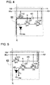
- FIG. 4 describes the operation of the pixel circuit
- FIG. 5 describes the operation of the pixel circuit
- FIG. 6 is a circuit diagram illustrating another example of the pixel circuit
- FIG. 7 is a circuit diagram illustrating another example of the pixel circuit
- FIG. 8 is a timing chart illustrating the operation of the pixel circuit
- FIG. 9 is a circuit diagram illustrating another example of the pixel circuit.
- FIG. 10 is a circuit diagram illustrating another example of the pixel circuit
- FIG. 11 is a timing chart illustrating the waveforms of signals supplied to the pixel circuit
- FIG. 12 is a circuit diagram illustrating the structure of the pixel circuit at a first time
- FIG. 13 is a circuit diagram illustrating the structure of the pixel circuit at a second time
- FIG. 14 is a circuit diagram illustrating the structure of the pixel circuit at a driving time
- FIG. 15 is a circuit diagram illustrating another example of the pixel circuit
- FIG. 16 is a timing chart illustrating the waveforms of signals supplied to the pixel circuit
- FIG. 17 is a circuit diagram illustrating the structure of the pixel circuit at a first time
- FIG. 18 is a circuit diagram illustrating the structure of the pixel circuit at a second time
- FIG. 19 is a circuit diagram illustrating the structure of the pixel circuit at a driving time
- FIG. 20 is a timing chart illustrating the waveforms of signals according to another aspect
- FIG. 21 is a circuit diagram illustrating another example of the pixel circuit
- FIG. 22 is a timing chart illustrating the waveforms of signals supplied to the pixel circuit
- FIG. 23 illustrates a personal computer using the light emitting device
- FIG. 24 illustrates a mobile telephone using the light emitting device
- FIG. 25 illustrates a portable information terminal using the light emitting device.
- FIG. 1 is a block diagram illustrating the schematic structure of an electro-optical device including an organic electroluminescence (EL) device (hereinafter, referred to as an OLED device) according to an embodiment of the present invention.
- FIG. 2 is a circuit diagram of a pixel circuit.
- a light emitting device 1 includes a pixel area A, a scan line driving circuit 100 , a data line driving circuit 200 , a control circuit 300 , and a power supply circuit 500 .
- m scan lines 101 and m power supply lines L that run parallel to the X direction are formed in the pixel area A.
- n data lines 103 that run parallel to the Y direction that intersects the X direction are formed.
- One pixel circuit 400 is provided to correspond to each of the intersections between the scan lines 101 and the data lines 103 .
- the pixel circuit 400 includes an OLED device 430 .
- a high electric potential power supply voltage Vdd as a power supply voltage is supplied to the pixel circuits 400 through the power supply lines L.
- the scan line driving circuit 100 supplies scan signals SEL 1 to SELm to the scan lines 101 , respectively.
- the scan line driving circuit 100 selects the scan lines 101 by one row every one horizontal scan time to sequentially supply the scan signals SEL 1 to SELm in response to the selection.
- the scan signal supplied to the ith (i is a natural number selected from 1 to m) scan line 101 is denoted by SELi.
- the data line driving circuit 200 supplies a data signal having a voltage in accordance with the voltage level of a driving voltage or the current level of a driving current to be supplied to the OLED device 430 of the corresponding pixel circuit 400 to each of the pixel circuits 400 corresponding to the scan line 101 selected by the scan line driving circuit 100 .
- the data signal (data voltage) sets the brightness of a pixel to increase according as a voltage is reduced and sets the brightness of the pixel to be reduced according as the voltage increases.
- the data signal supplied to the jth data line 103 is denoted by Xj.
- the control circuit 300 supplies clock signals (not shown) to the scan line driving circuit 100 and the data line driving circuit 200 to control the two driving circuits and to supply image data for determining the gradation of each pixel to the data line driving circuit 200 .
- the pixel circuit 400 will be described in detail with reference to FIG. 2 .
- the pixel circuit 400 illustrated in FIG. 2 corresponds to the ith row.
- the pixel circuit 400 includes a p channel type driving transistor 410 , a first n channel type transistor 412 that functions as a first switching device, a second p channel type transistor 414 that functions as a second switching device, a capacitor 420 having a first electrode, a dielectric layer, and a second electrode, and an OLED device 430 that is a light emitting device.
- the OLED device 430 may emit light at the brightness corresponding to the current amount or the current level of the driving current that flows from the pixel electrode positioned in the driving transistor toward the opposite electrode facing the pixel electrode due to a light emitting layer inserted into the pixel electrode and being set to have the power supply voltage Vss of the lower voltage side with respect to the power supply voltage of the high voltage side.
- An EL material in accordance with an emission color is used for the emission layer.
- the driving transistor 410 and the second driving transistor 414 are serially connected to each other.
- the second electrode oppositely positioned by inserting the channel of the driving transistor 410 , of the driving transistor 410 , to which the OLED device 430 is connected is connected to the first electrode (drain electrode) of the second transistor 414 .
- the second terminal (source electrode) of the second transistor 414 is connected to the power supply line L and the high electric potential power supply voltage Vdd is applied to the second terminal of the second transistor 414 .
- the driving current flows to the OLED device 430 in the order of the high electric potential power supply voltage Vdd (power supply line L) ⁇ the second transistor 414 ⁇ the driving transistor 410 ⁇ the OLED device 430 ⁇ the low electric potential power supply voltage Vss.
- the opposite electrode having the low electric potential power supply voltage Vss may be common to a plurality of pixel electrodes.
- the gate electrode of the driving transistor 410 is connected to the first electrode of the capacitor 420 and the first terminal (source electrode) of the first transistor 412 .
- the second terminal (drain electrode) of the first transistor 412 is connected to the data line 103 .
- the second electrode of the capacitor 420 is connected to the power supply line L and the high electric potential power supply voltage Vdd is applied to the corresponding second electrode.
- a node N is formed between the first electrode of the capacitor 420 and the gate electrode of the driving transistor 410 .
- the source electrode and the drain electrode of a transistor are strictly defined by the level of the relative voltage between conduction type or channel-insertion type two electrodes of the corresponding transistor.
- the drain electrode D and the source electrode S of the first transistor 412 are defined as illustrated in FIG. 2 .
- the source electrode S and the drain electrode D are reversed.
- the node N of the first transistor 412 becomes the drain electrode and the data line 103 of the first transistor 412 becomes the source electrode.
- the drain electrode and the source electrode of the first transistor 412 are positioned as illustrated in FIG. 2 .
- the drain electrode of the first transistor 412 is connected to the jth data line 103 and the gate electrode of the first transistor 412 is connected to the ith scan line 101 . That is, the scan signal SELi is supplied to the gate electrode of the first transistor 412 through the scan line 101 .
- the scan signal SELi is at a high level (H level)
- the first transistor 412 is turned on and the data signal Xj is input to the capacitor 420 .
- the scan signal SELi is at a low level (L level)
- the first transistor 412 is turned off and the node N is electrically separated from the data line 103 . In this state, the accumulated charge of the capacitor 420 is maintained.
- the first transistor 412 is of an n channel type and the second transistor 414 is of a p channel type.
- the common scan signal SELi is supplied to the gate electrodes of the first and second transistors 412 and 414 .
- the scan signal SELi may be set so that, when one of the first transistor 412 and the second transistor 414 is turned on, the other of the first transistor 412 and the second transistor 414 is turned off. Therefore, when the data signal xj is written in the capacitor 420 , it is possible to intercept the driving current supplied to the OLED device 430 .
- FIG. 3 is a timing chart describing the operation of the light emitting device 1 .
- the scan line driving circuit 100 sequentially selects first, second, third, . . . , and mth scan lines 101 every horizontal scan time ( 1 H) from the start of one vertical scan time ( 1 F) so that only the scan signal of the selected scan line 101 is at the H level and the scan signals of the other scan lines are at the L level.
- the operation of the pixel circuit 400 in the ith row and jth column may be divided into an operation at a writing time T WRT and an operation at an emission time T EL .
- the operations in the above-described times will be described in the order.
- the data signal Xj is written in the pixel circuit 400 .
- the scan line driving circuit 100 makes the scan signal SELi be at the H level. Therefore, in the pixel circuit 400 , as illustrated in FIG. 4 , the first transistor 412 is turned on and the second transistor 414 is turned off by the scan signal SELi at the H level.
- the data line driving circuit 200 supplies the data signal Xj of the data voltage in accordance with the gradation of the pixel in the ith row and jth column to the pixel circuit 400 through the data line 103 .
- the data voltage of the data signal Xj is determined as Vdata
- the voltage of the node N becomes Vdata.
- the voltage of the power supply line L may be reduced when the driving current starts to flow by wiring line resistance even at the writing time T WRT .
- the power supply voltage Vdd is reduced.
- the second transistor 414 since the second transistor 414 is certainly turned off at the writing time T WRT so that the driving current does not flow, it is possible to prevent the power supply voltage Vdd from being reduced.
- the driving current having the current level corresponding to the data signal Xj is supplied to the OLED device 430 so that light is emitted.
- the scan line driving circuit 100 makes the scan signal SELi be at the L level. Therefore, in the pixel circuit 400 , as illustrated in FIG. 5 , the first transistor 412 is turned off and the second transistor 414 is turned on by the scan signal SELi at the L level. Since the off resistance of the first transistor 412 and the gate input resistance of the driving transistor 410 are very high, the voltage of the node N is maintained as Vdata.
- the driving current I EL having the current level in accordance with the data voltage Vdata flows to the OLED device 430 through the second transistor 414 . Therefore, the OLED device 430 emits light with the brightness in accordance with the driving current I EL .
- the driving current I EL that flows to the OLED device 430 is obtained by the following Equation (1).
- I EL 1 ⁇ 2 ⁇ (Vgs ⁇ Vth) 2
- I EL 1 ⁇ 2 ⁇ (Vdd ⁇ Vdata) ⁇ Vth ⁇ 2 (1)
- Vgs and Vth represent a difference between the gate voltage and the source voltage of the driving transistor 410 and the threshold voltage of the driving transistor, respectively.
- the power supply voltage Vdd is reduced.
- the reduction in voltage is denoted by ⁇ V
- the power supply voltage becomes (Vdd ⁇ V).
- the node N floats, when the power supply voltage is reduced by ⁇ V, the voltage of the node N is also reduced by ⁇ V by the capacity coupling that is performed through the capacitor 420 . Therefore, in the Equation (1), Vdd becomes (Vdd ⁇ V), Vdata becomes (Vdata ⁇ V), and ⁇ V is canceled. Therefore, although the power supply voltage Vdd is reduced at the emission time T EL , it is possible to prevent the emission brightness of the OLED device 430 from being affected.
- the electric potential (Vdd) of the side connected to the power supply line L of the capacitor 420 is always made a predetermined electric potential.
- the power supply voltage Vdd change. The change is reflected to the gate voltage of the driving transistor 410 by the capacity coupling that is performed by the capacitor 420 . Also, the change in the power supply voltage Vdd is compensated for so that the driving current having the desired current level can be supplied to the OLED device 430 .
- the electric potential of the side connected to the power supply voltage Vdd of the capacitor 420 during the setting of the gate voltage of the driving transistor 410 is reduced.
- Reduction in the electric potential is particularly irregular when the plurality of power supply lines that intersect the plurality of scan lines 101 are arranged. That is, when the plurality of power supply lines that intersect the plurality of scan lines 101 are arranged, the electric potential of the side connected to the power supply voltage Vdd of the capacitor 420 of the pixel circuit in which the data voltage is written is affected by the current level of the driving current of the pixel circuit excluding the pixel circuit. This is because the current level of the driving current temporally changes in accordance with display contents.
- the second transistor 414 since the second transistor 414 is turned off at the writing time T WRT as described above, current is prevented from flowing to the pixel circuit 400 and the plurality of power supply lines L are arranged to intersect the plurality of data lines 103 or are arranged along the plurality of scan lines 101 . Therefore, the power supply voltage Vdd is prevented from being reduced at the writing time T WRT and the change in the power supply voltage Vdd is directly reflected to the gate voltage of the driving transistor 410 at the emission time T EL . As a result, the change in the power supply voltage Vdd is compensated for so that the driving current having the desired current level can be supplied to the OLED device 430 .
- the plurality of power supply lines L are arranged to intersect the plurality of data lines 103 along the plurality of scan lines 101 , the plurality of pixel circuits 400 arranged in one row are connected to one power supply line L.
- the ith scan line is selected, data voltages are input from the data lines 103 to all of the pixel circuits 400 arranged in the ith row.
- the first transistor 412 is turned on and the second transistor 414 is turned off, the path through which the driving current I EL is supplied to the OLED device 430 is intercepted at the writing time T WRT in each of the pixel circuits 400 in the ith row. Therefore, the power supply voltage Vdd of the power supply line L is prevented from being reduced at the writing time T WRT so that the difference Vgs between the gate voltage and the source voltage can be correctly set with respect to each of the pixel circuits 400 .
- the power supply line provided around the pixel area A may be referred to as a main power supply line and the plurality of power supply lines provided in the pixel area A in the row direction may be referred to as auxiliary power supply lines.
- the width of the auxiliary power supply lines is made smaller than the width of the main power supply line so that the aperture ratio of the OLED device 430 is improved.
- the reduction in the power supply voltage Vdd is mostly generated by the auxiliary power supply lines.
- the pixel circuits 400 connected to the other scan lines 101 are at the emission time so that the driving current I EL flows to the pixel circuits 400 .
- the auxiliary power supply lines are arranged in the row direction so that it is possible to prevent the driving current from changing due to the reduction in the power supply voltage Vdd.
- the OLED device 430 is formed of a light emitting organic material such as monomer, polymer, and dendrimer.
- the OLED device 430 is an example of the current driving device.
- the driving circuit according to the above embodiment may be used for a voltage driving device.
- an inorganic EL device, a field emission (FE) device, a surface conduction electron emitter (SE) device, a ballistic electron surface emitting (BS) device, an electrophoresis device, or an electrochromic device can be used as the driven device of the driving circuit according to the embodiment.
- the driving circuit according to the embodiment can be used as the driving circuit of the electro-optical device such as a recording head used for an optical recording printer or electronic photocopier.
- the driving circuit according to the present embodiment can be applied to a sensing device in which an object to be examined is detected by measuring a current level or a voltage level such as a biochip.
- FIG. 6 is a circuit diagram illustrating another example of the pixel circuit.
- the positions of the driving transistor 410 and the second transistor 414 of the pixel circuit 400 illustrated in FIG. 2 are reversed. That is, the second transistor 414 is connected between the driving transistor 410 and the OLED device 430 and the operation of the pixel circuit 400 A is almost the same as the writing operation and the emission operation according to the above-described embodiment. That is, the second transistor 410 is preferably formed on the path through which the driving current I EL is supplied to the OLED device 430 .
- FIG. 7 is a circuit diagram illustrating another example of the pixel circuit.
- the turning on and off of the second transistor 414 is controlled by the scan signal SELi for controlling the first transistor 412 .
- the second transistor 414 is controlled by a control signal Gi.
- m control lines 102 are formed to run parallel to the m scan lines 101 and the scan line driving circuit 100 generates control signals G 1 to Gm other than the scan signals SEL 1 to SELm to supply the control signals G 1 to Gm to the control lines 102 , respectively.
- the turning on and off of each of the first transistor 412 and the second transistor 414 is independently controlled.
- FIG. 8 is a timing chart of the pixel circuit 400 B illustrated in FIG. 7 .
- the operation of the pixel circuit 400 in the ith row and jth column is divided into an operation at the writing time T WRT , an operation in an idle time T OFF , and an operation at the emission time T EL .
- the time at which the scan signal SELi is at the H level is as illustrated in the above-described embodiment, which is the writing time T WRT .
- the pulse width of the control signal Gi at the H level is larger than the pulse width of the scan signal SELi at the H level. That is, since the control signal Gi is deactivated for the time longer than the time for which the scan signal SELi is activated.
- the idle time T OFF when the scan signal SELi is at the L level and the control signal Gi is at the H level, the first transistor 412 and the second transistor 414 are turned off. Therefore, in the idle time T OFF , the data signal Xj is not input to the pixel circuit 400 and the OLED device 430 does not emit light.
- the idle time T OFF is formed between the writing time T WRT and the emission time T EL so that a margin is generated. Therefore, it is possible to prevent the writing time T WRT and the emission time T EL from overlapping each other. That is, it is possible to prevent the driving current from flowing between the power supply line L and the opposite electrode having the low electric potential power supply voltage Vss at the writing time T WRT .
- the scan signal SELi is supplied to the n pixel circuits 400 arranged in the ith row through the ith scan line 101 . Since parasitic capacity is generated in the scan line 101 , a trapezoidal low pass filter is equivalently formed in the scan line 101 . Therefore, when the scan signal SELi is supplied from one end of the ith scan line 101 , the scan signal SELi supplied to the pixel circuit 400 B connected to the other end of the ith scan line 101 is delayed compared with the scan signal SELi supplied to the pixel circuit 400 B connected to one end of the ith scan line 101 .
- FIG. 9 is a circuit diagram illustrating another example of the pixel circuit.
- the pixel circuit 400 C in the ith row is illustrated.
- the structure of the pixel circuit 400 C is the same as the structure of the pixel circuit 400 according to the above-described embodiment excluding that the second transistor 414 is common to the plurality of pixel circuits 400 C.
- the second transistor 414 according to the example is electrically connected between a main power supply line La provided in the column direction and an auxiliary power supply line Lb provided in the row direction.
- the turning on and off of the second transistor 414 is controlled by the control signal Gi.
- the control signal Gi is at the H level at the writing time T WRT and the control signal Gi is at the L level at the emission time T EL .
- the power supply voltage Vdd is supplied to the pixel circuits 400 C at the emission time T EL .
- the plurality of pixel circuits 400 C share the second transistor 414 , it is possible to simplify the structure of the pixel circuit or the light emitting device 1 .
- the structure of the pixel circuit 400 will be described with reference to FIG. 10 .
- FIG. 10 only the jth (j is an integer that satisfies 1 ⁇ j ⁇ n) pixel circuit 400 that belongs to the ith (i is an integer that satisfies 1 ⁇ i ⁇ m) row is illustrated.
- the other pixel circuits 400 have the same structure.
- the conduction type of the transistor that constitutes the pixel circuit 400 is not limited to the example of FIG. 10 .
- the transistor illustrated in FIG. 10 is a thin film transistor (TFT) obtained by using low temperature poly silicon for a semiconductor layer.
- TFT thin film transistor
- the shape and material of the transistor are not limited.
- the pixel circuit 400 includes an OLED device 420 and a p channel type transistor (hereinafter, a driving transistor) Qdr that are interposed between a power supply line 31 to which the power supply voltage Vdd is supplied and an opposite electrode 32 to which a ground voltage Vss is supplied.
- the OLED device 430 may emit light at the brightness corresponding to the current amount or the current level of the driving current that flows from the pixel electrode positioned in the driving transistor toward the opposite electrode 32 facing the pixel electrode due to a light emitting layer inserted into the pixel electrode and being set to have the power supply voltage Vss of the lower voltage side with respect to the power supply voltage of the high voltage side.
- An EL material in accordance with an emission color is used for the emission layer.
- the driving transistor Qdr is a transistor for controlling the current level of the driving current or the voltage level of the driving voltage that is supplied to the OLED device 430 .
- the driving circuit according to the present embodiment is suitable for a driven device that is mainly driven by current such as the OLED device 430 .
- a voltage driven device that is mainly driven by a voltage such as an inorganic EL device, a field emission (FE) device, a surface conduction electron emitter (SE) device, a ballistic electron surface emitting (BS) device, an electrophoresis device, or an electrochromic device can be used as the driven device.
- the driving circuit according to the embodiment can be used as the driving circuit of the electro-optical device such as a recording head used for an optical recording printer or electronic photocopier.
- the driving circuit according to the present embodiment can be applied to a sensing device in which an object to be examined is detected by measuring a current level or a voltage level such as a biochip.
- the scan line 10 illustrated as one wiring line for convenience sake in FIG. 1 actually includes a first control line 11 and a second control line 12 as illustrated in FIG. 10 .
- First control signals Sa 1 [ 1 ] to Sa 1 [m] for determining the time for inputting the data voltage Vdata to the pixel circuit 400 are supplied from the scan line driving circuit 100 to the first control line 11 of each row.
- second control signals Sa 2 [ 1 ] to Sa 2 [m] for determining the time for initializing the voltage maintained in the pixel circuit 400 are supplied from the scan line driving circuit 100 to the second control line 12 of each row.
- the detailed waveforms of the signals and the operations of the pixel circuit 400 in accordance with the waveforms will be described later.
- a first transistor Qa 1 illustrated in FIG. 10 is a p channel type transistor connected between the driving transistor Qdr and the power supply line 31 .
- the first transistor Qa 1 and the driving transistor Qdr are serially connected to each other and the first transistor Qa 1 functions as a switching device for controlling electric connection between the driving transistor Qdr and the power supply line 31 .
- the emission control transistor Qe 1 illustrated in FIG. 10 is a p channel type transistor connected between the driving transistor Qdr and the OLED device 430 and functions as a switching device for controlling electric connection between the driving transistor Qdr and the OLED device 430 .
- the gate electrodes of the first transistor Qa 1 and the emission control transistor Qe 1 are connected to the first control line 11 .
- the first control signal Sa 1 [i] when the first control signal Sa 1 [i] is properly set, it is possible to set both of the first transistor Qa 1 and the emission control transistor Qe 1 to operate.
- the first transistor Qa 1 and the emission control transistor Qe 1 are turned off when the first control signal Sa 1 [i] is at the H level and are turned on when the first control signal Sa 1 [i] is at the L level.
- the second transistor Qa 2 illustrated in FIG. 10 is an n channel type transistor connected between the gate of the driving transistor Qdr and the first transistor Qa 1 .
- the third transistor Qa 3 illustrated in FIG. 10 is an n channel type transistor connected between the driving transistor Qdr and the data line 103 and functions as a switching device for switching conduction and non-conduction of the driving transistor Qdr and the data line 103 .
- the gate electrodes of the second transistor Qa 2 and the third transistor Qa 3 are connected to the first control line 11 . Therefore, the second transistor Qa 2 and the third transistor Qa 3 are turned on when the first control signal Sa 1 [i] is at the H level and are turned off when the first control signal Sa 1 [i] is at the L level.
- the second transistor Qa 2 When the second transistor Qa 2 is turned on, electricity flows through the gate electrode and the source electrode of the driving transistor Qdr so that the driving transistor Qdr functions as a diode.
- the capacitor C 0 illustrated in FIG. 10 is a capacitor for maintaining a charge between a first electrode L 0 a and a second electrode L 0 b .
- the first electrode L 0 a is connected to the gate electrode of the driving transistor Qdr and the second electrode L 0 b is connected to the power supply line 31 .
- a fourth transistor Qa 4 is connected to the connection point N G between the first electrode L 0 a of the capacitor C 0 and the gate electrode of the driving transistor Qdr.
- the fourth transistor Qa 4 is a n channel type transistor connected between the first electrode L 0 a and the ground voltage Vss and functions as a switching device for controlling electric connection between the first electrode L 0 a or the connection point N G and the ground voltage Vss (typically, for switching conduction and non-conduction of the first electrode L 0 a and the ground voltage Vss).
- the gate electrode of the fourth transistor Qa 4 is connected to the second control line 12 . Therefore, the fourth transistor Qa 4 is turned on when the second control signal Sa 2 [i] is at the H level and is turned off when the second control signal Sa 2 [i] is at the L level.
- the first control signals Sa 1 [ 1 ] to Sa 1 [m] are signals sequentially transited to the H level every horizontal scan time ( 1 H). That is, the first control signal Sa 1 [i] maintains the H level in the ith horizontal scan time in the vertical scan time ( 1 V) and maintains the L level in the other time.
- the transition of the first control signal Sa 1 [i] to the H level means that the pixel circuits 400 in the ith row are selected. As illustrated in FIG.
- the data voltage Vdata corresponding to the gradation of the pixel circuits 400 in the ith row is supplied to the data line 103 .
- the data voltage Vdata is input to the pixel circuits 400 through the third transistor Qa 3 that is turned on by the first control signal Sa 1 [i] at the H level.
- the time (that is, horizontal scan time) at which the first control signals Sa 1 [ 1 ] to Sa 1 [m] are at the H level is referred to as the writing time T WRT .
- the time other than the writing time T WRT (that is, the time at which the first control signals Sa 1 [ 1 ] to Sa 1 [m] are at the L level) is referred to as the time (hereinafter, the driving time T EL ) at which the driving current having the current level in accordance with the data voltage Vdata is supplied to the OLED device 430 .
- the writing time T WRT at which the first control signal Sa 1 [i] is at the H level is divided into a first time T 1 , and a second time T 2 .
- the first time T 1 starts from the point of time of the writing time T WRT and lasts until a predetermined time passes.
- the second time T 2 is the remaining time of the corresponding writing time T WRT .
- the second control signal Sa 2 [i] maintains the H level at the first time T 1 and maintains the L level at the other times (that is, the second time T 2 and the driving time T EL ).
- the connection point N G and the ground voltage Vss of FIG. 10 are electrically connected to each other through the fourth transistor Qa 4 that is turned on.
- the operation of the pixel circuit 400 in the first row and the jth column will be divided into an operation at the first time T 1 , an operation at the second time T 2 , and an operation at the driving time T EL to be described.
- FIG. 12 is a circuit diagram equivalently illustrating the electric structure of the pixel circuit 400 .
- the connection point N G that is, the gate electrode of the driving transistor Qdr
- the fourth transistor Qa 4 is electrically connected to the ground voltage Vss through the fourth transistor Qa 4 that is turned on, as illustrated in FIG.
- the voltage V G of the connection point N G is reduced to the ground voltage Vss at the first time T 1 .
- the first time T 1 illustrated in FIG. 11 is set to be long enough for the voltage V G of the connection point N G to reach the ground voltage Vss.
- the second transistor Qa 2 , the third transistor Qa 3 , and the fourth transistor Qa 4 are turned on, in at least a part of the first time T 1 , current flows between the data line 103 and the ground electric potential 32 through the fourth transistor Qa 4 , the second transistor Qa 2 , and the driving transistor Qdr.
- the current operates as a kind of pre-charge current to rapidly set the gate voltage of the driving transistor Qdr by the data voltage Vdata.
- the starting point of time at which the fourth transistor Qa 4 is turned on and the starting point of time at which the second transistor Qa 2 and the third-transistor Qa 3 are turned on are formed so that the pre-charge effect is obtained by the current as described above.
- FIG. 13A is a circuit diagram equivalently illustrating the electric structure of the pixel circuit 400 .
- the fourth transistor Qa 4 is turned off so that the connection point N G is electrically separated from the ground voltage Vss.
- the second transistor Qa 2 is turned on so that electricity flows through the driving transistor Qdr and that the driving transistor Qdr functions as a diode.
- the second time T 2 is set to be long enough for the voltage V G of the connection point N G to reach the level (Vdata ⁇ Vth) from the point of time at which the second transistor Qa 2 and the third transistor Qa 3 are turned on.
- the first control signal Sa 1 [i] maintains the H level so that the first transistor Qa 1 and the emission control transistor Qe 1 are turned off. Therefore, the power supply line 31 and the driving transistor Qdr are electrically insulated from each other and the path of the current that is transmitted from the power supply line 31 to the opposite electrode 32 through the OLED device 430 is intercepted.
- the difference Vgs between the gate voltage and the source voltage is maintained with a high precision degree in the capacitor C 0 interposed between the power supply line 31 and the connection point N G .
- FIG. 14 illustrates a circuit illustrating an equivalent structure of the pixel circuit 400 at this time. As shown in the drawing, the first transistor Qa 1 and the light emitting control transistor Qe 1 are transited to ON state so that a path from the power supply line 31 to the opposite electrode 32 via the driving transistor Qdr and the OLED device 430 is formed.
- the driving current Ie 1 flowing from the power supply line 31 to the OLED device 430 has a current level according to the data voltage Vdata. Therefore, the OLED device 430 emits light at the brightness corresponding to the data voltage Vdata.
- the driving current Ie 1 flowing from the source electrode of the driving transistor Qdr to the drain electrode is expressed by the following equation (2).
- I e1 (1 ⁇ 2) ⁇ (Vgs ⁇ Vth) 2 (2)
- Vgs is a voltage between the gate and the source of the driving transistor Qdr
- ⁇ is a gain coefficient of the driving transistor Qdr.
- the driving current Ie 1 is not dependent on the threshold voltage Vth of the driving transistor Qdr. Therefore, according to the present embodiment, characteristic unbalance such as the threshold voltage Vth of the driving transistor Qdr in each pixel circuit 400 is compensated so that the OLED device 430 can emit light at a desired brightness with a high precision.
- the power supply voltage Vdd is dropped. If the dropped value of the voltage at this time is set to ⁇ V, the power supply voltage after the voltage drop is Vdd ⁇ V. Since the connection point N G at the driving time T EL is the floating state, when the power supply voltage Vdd is dropped by ⁇ V, the voltage at the connection point N G is basically dropped by ⁇ V. Therefore, since Vdd becomes Vdd ⁇ V in the equation (3) and Vdata in the same equation becomes Vdata ⁇ V, the influence by the voltage drop of the power supply voltage Vdd with respect to the driving current Ie 1 is therefore canceled. In other words, the voltage drop of the power supply voltage Vdd at the driving time T EL does not give influence the brightness of the OLED device 430 .
- the respective power supply lines 31 are formed along the arrangement direction of the respective pixels selected by the scan line driving circuit 100 at once (in other words, the direction of the arrangement of the pixels for simultaneously executing the insertion), the voltage drop of the power supply voltage Vdd at the writing time T WRT can be securely prevented. This advantage will be described in detail as follows.
- the path of the driving current Ie 1 is intercepted by turning the first transistor Qa 1 or the light emitting control transistor Qe 1 of the ith pixel circuit 400 OFF at the writing time T WRT since the driving current Ie 1 is supplied to the OLED device 430 of the pixel circuit 400 belonging to other rows (in other words, the pixel circuit 400 at the driving time T EL ), the power supply voltage Vdd of the power supply lines 31 in the respective rows is dropped.
- the power supply line 31 is formed in the raw direction like the present embodiment, when the respective ith pixel circuits 400 commonly connected to a single power supply line 31 is selected by the scan line driving circuit 100 , the insertion of the data voltage Vdata into the number n of the pixel circuits 400 is performed at once. Therefore, due to the supply of the driving current Ie 1 to the OLED device 430 , the power supply voltage Vdd of the power supply line 31 is prevented from dropping so that the data voltage Vdata can be precisely inserted into the respective pixel circuits 400 .
- wires for supplying the power supply voltage Vdd from the power supply circuit 500 to the respective pixel circuits 400 includes a main power supply line disposed surrounding a pixel area A and an auxiliary power supply line extending in the pixel circuit 400 in the raw direction.
- the auxiliary power supply line in view of sufficiently securing an area (aperture ratio) where the respective OLED devices 430 emit light, is formed by a narrow line width by comparison to the main power supply line. Therefore, a majority of the voltage drop of the power supply voltage is generated in the auxiliary power supply line.
- the driving current Ie 1 flows into the respective OLED devices 430 .
- the majority of resistance of the power supply line 31 is in the auxiliary power supply line, when the auxiliary power supply line is formed in the raw direction like the present embodiment, it can be obtained a secure effect that the voltage drop of the power supply voltage Vdd is improved.
- FIG. 15 illustrates a circuit illustrating the structure of other pixel circuit related to the present embodiment.
- the pixel circuit 401 of the present embodiment like the first embodiment, includes the OLED devices disposed between the power supply line 31 and the opposite electrode 32 and the p-channel type driving transistor Qdr. Between the driving transistor Qdr and the OLED device 430 , the n-channel type light emitting control transistor Qe 1 is disposed. The gate electrode of the light emitting control transistor Qe 1 is connected to a first control line 11 through which the first control signal Sb 1 [i] is supplied. Meanwhile, the source electrode of the driving transistor Qdr is connected to the source electrode of the first transistor Qb 1 .
- the first transistor Qb 1 is an n-channel type transistor having a drain electrode connected to the power supply line 31 , and serves as a switching device for switching the electric conduction and non-conduction between the source electrode of the driving transistor Qdr and the power supply line 31 .
- the gate electrode of the first transistor Qb 1 is connected to the second control line 12 through which the second control signal Sb 2 [i] is supplied.
- the second transistor in FIG. 15 is a p-channel type transistor connected between the gate electrode of the driving transistor Qdr and any one of the drain electrode and the source electrode of the driving transistor Qdr.
- the gate electrode of the second transistor Qb 2 is connected to a first control line 11 .
- the first electrode L 1 a of the first capacitor C 1 and the first electrode L 2 a of the second capacitor C 2 are connected to the gate electrode of the driving transistor Qdr.
- the second electrode L 2 b of the second capacitor C 2 is connected to the power supply line 31 .
- the second electrode L 1 b of the first capacitor C 1 is connected to the drain electrode of the third transistor Qb 3 .
- the third transistor Qb 3 is a switching device for controlling the electrical connection between the data line 103 and the second electrode L 1 b of the first capacitor C 1 (typically, switching conduction and non-conduction therebetween), the source electrode thereof is connected to the data line 103 , and the gate electrode thereof is connected to the first control line 11 .
- the voltage, supplied to the electrodes of the respective transistors varies suitable for the operating state.
- the source electrodes and the drain electrodes are strictly changed to each other according to the operation state.
- one side electrodes of the respective transistors are assigned to the source electrodes and other electrodes are assigned to the drain electrodes.
- FIG. 16 is a timing chart illustrating the waveforms of first control signals Sb 1 [ 1 ] to Sb 1 [m] and second control signals Sb 2 [ 1 ] to Sb 2 [m] in the present embodiment.
- the ith horizontal scan time 1 H of the respective vertical scan time 1 V is used as the writing time T WRT when the compensation of the threshold voltage Vth of the driving transistor Qdr and the insertion of the data voltage Vdata are performed in the respective pixel circuits 401 in the ith raw, and other time is used as the driving time T EL when OLED devices 430 of the respective pixel circuits 401 illuminate.
- the first control signals Sb 1 [ 1 ] to Sb 1 [m] are signals that are sequentially low level for every writing time T WRT when the respective rows are selected.
- the first control signals Sb 1 [ 1 ] to Sb 1 [m] become L-level for the writing time T WRT when the ith raw is selected, and become H-level for other time (the driving time T EL corresponding to the ith raw).
- the writing time T WRT is distinguished into a first time T 1 for compensating the threshold voltage Vth of the driving transistor Qdr and a second time T 2 for inserting the data voltage Vdata into the pixel circuit 401 . As shown in FIG.
- the second control signals Sb 2 [ 1 ] to Sb 2 [m] become low level for the second time T 2 among the writing time T WRT when the first control signals Sb 1 [m] to Sb 1 [m] become L-level, and become L-level for other time (the driving time T EL and the first time T 1 ).
- the operation of the pixel circuit 401 will be described separately for the first time T 1 and the second time T 2 of the writing time T WRT and the driving time T EL . Moreover, hereinafter, although operation of the jth pixel circuit 401 of the ith raw will be specifically described, other pixel circuits 401 are like that.
- a predetermined voltage Vref (hereinafter referred to “reference voltage”) is applied.
- the reference voltage Vref is applied to the second electrode L 1 b of the first capacitor C 1 through the turned on third transistor Qb 3 .
- the reference voltage Vref for example, is Vss or Vdd.
- the data voltage Vdata based on the gradation of the pixel circuit 401 in the ith raw is applied to the data line 103 .
- the third transistor Qb 3 at this time is turned on by the low-level first control signal Sb 1 [i]
- the data voltage Vdata is applied to the second electrode L 1 b of the first capacitor C 1 through the third transistor Qb 3 .
- the voltage of the second electrode L 1 b varies from the reference voltage Vref determined in the first time T 1 to the data voltage Vdata.
- the voltage V G of the gate electrode of the driving transistor Qdr varies as much as a level that the voltage variation ⁇ V at the second electrode L 1 b is divided by the capacity coupling between the first capacitor C 1 and the second capacitor C 2 , according to the ratio between the electrostatic capacity Ca of the first capacitor C 1 and the electrostatic capacity of the second capacity C 2 , from the immediately before voltage Vdd ⁇ Vth. Since the variation of the voltage V G at the connection point N G is expressed by ⁇ V ⁇ Ca/(Ca+Cb), the voltage V G of the connection point N G for the second time T 2 is stabilized by the level expressed by the following equation (4).
- V G Vdd ⁇ Vth ⁇ V ⁇ Ca/(Ca+Cb) (4)
- the voltage of the second electrode L 1 b is determined as the predetermined reference voltage Vref, the voltage V G of the gate electrode of the driving transistor Qdr for the second time T 2 can be rapidly determined to the level according to the data voltage Vdata.
- both of the first control signal Sb 1 [i] and the second control signal Sb 2 [i] becomes H-level. Therefore, as shown in FIG. 19 , the second transistor Qb 2 and the third transistor Qb 3 are turned off. Meanwhile, since all of the first transistor Qb 1 and the light-emitting transistor Qe 1 is turned on, a path from the power supply line 31 to the opposite electrode 32 via the driving transistor Qdr and the OLED device 430 is formed.
- the driving Ie 1 caused by the voltage between the gate and the source of the driving transistor Qdr is supplied to the OLED device 430 .
- the driving current Ie 1 is expressed by the following equation (5).
- I e 1 (1 ⁇ 2) ⁇ (Vdd ⁇ V G ⁇ Vth) 2 (5)
- an idle time T OFF may be inserted between the writing time T WRT and the driving time T EL .
- the idle time is a time period when the insertion of the data voltage Vdata with respect to the pixel circuit 401 and the supply of the driving current Le 1 to the OLED device 430 are not carried out.
- the second control signal Sb 2 [i] in this aspect as shown in FIG.
- the writing time T WRT and the driving time T EL may be overlapped with the driving time T EL caused by the delay or wave distortion of the first control signal Sb 1 [i] or the second control signal Sb 2 [i] (in other words, when the insertion of the data into the pixel circuit 401 and the supply of the driving current Ie 1 to the OLED device 430 are simultaneously performed), according to the aspect as shown in FIG. 20 , the situation when the driving current Ie 1 is supplied to the OLED device 430 during the insertion of the data voltage Vdata into the pixel circuit 401 can be securely prevented.
- FIG. 21 is a circuit diagram illustrating the structure of other pixel circuit according to the present embodiment.
- the first transistor Qb 1 of the pixel circuit 31 in FIG. 15 is eliminated.
- the driving transistor Qdr is directly connected to the power supply line 31 .
- the gate electrode of the light-emitting control transistor Qe 1 disposed between the driving transistor Qdr and the OLED device 430 is connected to the power supply line 13 . Therefore, the light emitting control transistor Qe 1 turns ON when the third control signal Sc 3 [i] supplied to the third control line 13 is H-level, and turns OFF when the third control signal Sc 3 [i] is L-level.
- the pixel circuit 402 in the present embodiment includes, instead of the second transistor Qb 2 of the pixel circuit 401 and the third transistor Qb 3 in FIG. 15 , n-channel type second transistor Qc 2 and n-channel type Qc 3 .
- a gate electrode of the second transistor Qc 2 is connected to the second control line 12 through which the second control signal Sc 2 [i] is supplied
- a gate electrode of the third transistor Qc 3 is connected to the first control line 11 through which the first control signal Sc 1 [i] is supplied.
- FIG. 22 is a timing chart illustrating waveforms of respective signals supplied to the pixel circuit 402 .
- the first control signal Sc 1 [i] to Sc 1 [m] sequentially become H-level in every horizontal scan time 1 H.
- the writing time T WRT horizontal scan time
- the second control signal Sc 2 [i] is at H-level during time from time point immediately before the writing time T WRT by a predetermined time to the ending point of the first time T 1 and is at L-level in other time. Operation in the first time T 1 and the second time T 2 is identical to that in FIG. 15 .
- the reference voltage is applied to the second electrode Lb 1 of the capacitor C 1 from the data line 103 via the third transistor Qc 3 turned ON by the high level first control signal Sc 1 [i] and the second transistor Qc 2 is turned ON by the high level second control signal Sc 2 [i] so that the voltage V G of the gate electrode of the driving transistor Qdr is converged to Vdd ⁇ Vth.
- the second time T 2 after the second transistor Qc 2 is turned OFF, the data voltage Vdata is applied to the second electrode L 1 b of the first capacitor C 1 so that the voltage V G of the driving transistor Qdr is set to a level according to the data voltage Vdata.
- the third control signals Sc 3 [ 1 ] to Sc 3 [m] are signals for defining the driving time T EL when the OLED device 430 actually emits light according to the data voltage Vdata inserted into the pixel circuit 402 at the writing time T WRT .
- a path from the power supply line 31 to the OLED device 430 is formed when the light-emitting control transistor Qe 1 is turned ON, and through this path, the driving current Ie 1 according to the voltage V G of the gate electrode of the driving transistor Qdr is supplied to the OLED device 430 .
- the third control signal Sc 3 [i] in the present embodiment goes up to the H-level at a time point when the idle time T OFF elapses after the first control signal Sc 1 [i] goes down to the low level.
- the idle time T OFF is inserted between the writing time T WRT and the driving time T EL .
- the idle time T OFF is a time period when the insertion of the data voltage Vdata into the pixel circuit 402 and the supply of the driving current Ie 1 to the OLED device 430 are not performed.
- any one of the first control signal Sc 1 [i], the second control signal Sc 2 [i], and the third control signal Sc 3 [i] become the L-level. Therefore, in the idle time T OFF , any one of the light emitting transistor Qe 1 , the second transistor Qc 2 , and the third transistor Qc 3 is turned OFF.
- the idle time T OFF is inserted between the writing time T WRT and the driving time T EL , the situation that the driving current Ie 1 is supplied to the OLED device 430 during the insertion of data into the pixel circuit 402 is securely prevented. Therefore, the voltage drop in the power supply line 31 is restrained so that a desired data voltage Vdata can be recorded into the pixel circuit 402 in high precision.
- FIG. 23 illustrates a mobile personal computer employing the light emitting device 1 .
- the personal computer 2000 includes the light emitting device 1 as a display unit and a main body 2010 .
- a power switch 2001 and a keyboard 2002 are installed in the main body 2010 .
- the light emitting device 1 can display an image with a wide viewing angle and convenient to watch because of using the OLED device 430 .
- FIG. 24 illustrates the structure of a mobile phone employing the light emitting device 1 .
- a mobile phone 3000 includes a plurality of manipulation buttons 3001 , scroll buttons 3002 , and the light emitting device 1 as a display unit.
- the scroll buttons 3002 are manipulated to scroll an image displayed on the light emitting device 1 .
- FIG. 25 illustrates a personal digital assistant (PDA) employing the light emitting device 1 .
- the PDA 400 includes a plurality of manipulation buttons 4001 , a power switch 4002 , and the light emitting device 1 as a display unit.
- various information items such as an address book, a schedule table, or the like are displayed on the light emitting device 1 .
- an electronic apparatus employing the light emitting device 1 other than that in FIGS.
- the light emitting device 1 can be employed in the various electronic apparatuses as a display unit. Moreover, without limit as a display unit of an electronic apparatus for displaying images and letters, the light emitting device may be uses as a light source of a printing apparatus uses in projecting light to photo sensitive object to form images or letters thereon indirectly.
Landscapes
- Engineering & Computer Science (AREA)
- Physics & Mathematics (AREA)
- Computer Hardware Design (AREA)
- General Physics & Mathematics (AREA)
- Theoretical Computer Science (AREA)
- Control Of Indicators Other Than Cathode Ray Tubes (AREA)
- Control Of El Displays (AREA)
- Electroluminescent Light Sources (AREA)
Abstract
Description
IEL=½β(Vgs−Vth)2
IEL=½β{(Vdd−Vdata)−Vth}2 (1)
Ie1=(½)β(Vgs−Vth)2 (2)
Ie1=(½)β(Vdd−Vdata)2 (3)
VG=Vdd−Vth−ΔV·Ca/(Ca+Cb) (4)
Ie1=(½)β(Vdd−VG−Vth)2 (5)
Ie1=(½)β(k·ΔV)2 (6)
Claims (8)
Priority Applications (2)
| Application Number | Priority Date | Filing Date | Title |
|---|---|---|---|
| US12/757,551 US8913044B2 (en) | 2005-04-15 | 2010-04-09 | Electronic circuit, method of driving the same, electro-optical device, and electronic apparatus |
| US14/550,706 US20150179104A1 (en) | 2005-04-15 | 2014-11-21 | Electronic circuit, method of driving the same, electro-optical device, and electronic apparatus |
Applications Claiming Priority (4)
| Application Number | Priority Date | Filing Date | Title |
|---|---|---|---|
| JP2005-117873 | 2005-04-15 | ||
| JP2005117873A JP2006300980A (en) | 2005-04-15 | 2005-04-15 | Electronic circuit, driving method thereof, electro-optical device, and electronic apparatus |
| JP2005-120774 | 2005-04-19 | ||
| JP2005120774A JP5392963B2 (en) | 2005-04-19 | 2005-04-19 | Electro-optical device and electronic apparatus |
Related Child Applications (1)
| Application Number | Title | Priority Date | Filing Date |
|---|---|---|---|
| US12/757,551 Division US8913044B2 (en) | 2005-04-15 | 2010-04-09 | Electronic circuit, method of driving the same, electro-optical device, and electronic apparatus |
Publications (2)
| Publication Number | Publication Date |
|---|---|
| US20070128583A1 US20070128583A1 (en) | 2007-06-07 |
| US7724245B2 true US7724245B2 (en) | 2010-05-25 |
Family
ID=37615672
Family Applications (3)
| Application Number | Title | Priority Date | Filing Date |
|---|---|---|---|
| US11/379,009 Active 2028-08-04 US7724245B2 (en) | 2005-04-15 | 2006-04-17 | Electronic circuit, method of driving the same, electro-optical device, and electronic apparatus |
| US12/757,551 Active 2028-02-19 US8913044B2 (en) | 2005-04-15 | 2010-04-09 | Electronic circuit, method of driving the same, electro-optical device, and electronic apparatus |
| US14/550,706 Abandoned US20150179104A1 (en) | 2005-04-15 | 2014-11-21 | Electronic circuit, method of driving the same, electro-optical device, and electronic apparatus |
Family Applications After (2)
| Application Number | Title | Priority Date | Filing Date |
|---|---|---|---|
| US12/757,551 Active 2028-02-19 US8913044B2 (en) | 2005-04-15 | 2010-04-09 | Electronic circuit, method of driving the same, electro-optical device, and electronic apparatus |
| US14/550,706 Abandoned US20150179104A1 (en) | 2005-04-15 | 2014-11-21 | Electronic circuit, method of driving the same, electro-optical device, and electronic apparatus |
Country Status (3)
| Country | Link |
|---|---|
| US (3) | US7724245B2 (en) |
| KR (2) | KR20060109343A (en) |
| TW (1) | TW200701167A (en) |
Cited By (11)
| Publication number | Priority date | Publication date | Assignee | Title |
|---|---|---|---|---|
| US20080225061A1 (en) * | 2006-10-26 | 2008-09-18 | Semiconductor Energy Laboratory Co., Ltd. | Electronic device, display device, and semiconductor device and method for driving the same |
| US20080284688A1 (en) * | 2004-06-11 | 2008-11-20 | Thilo Marx | Method for Driving, and a Circuit of an Element of an Illuminated Display |
| US20090159890A1 (en) * | 2007-12-21 | 2009-06-25 | Semiconductor Energy Laboratory Co., Ltd. | Semiconductor Display Device |
| US20100033475A1 (en) * | 2008-08-06 | 2010-02-11 | Samsung Electronics Co., Ltd. | Liquid crystal display and control method thereof |
| US8638279B2 (en) | 2010-08-02 | 2014-01-28 | Samsung Display Co., Ltd. | Pixel and organic light emitting display device using the same |
| US8710749B2 (en) | 2011-09-09 | 2014-04-29 | Semiconductor Energy Laboratory Co., Ltd. | Semiconductor device |
| US20140160179A1 (en) * | 2012-12-11 | 2014-06-12 | Samsung Display Co., Ltd. | Pixel circuit and display device |
| US9984617B2 (en) | 2010-01-20 | 2018-05-29 | Semiconductor Energy Laboratory Co., Ltd. | Display device including light emitting element |
| US10043794B2 (en) | 2012-03-22 | 2018-08-07 | Semiconductor Energy Laboratory Co., Ltd. | Semiconductor device and electronic device |
| US10885861B2 (en) | 2013-09-12 | 2021-01-05 | Semiconductor Energy Laboratory Co., Ltd. | Display device |
| US11694648B2 (en) | 2017-09-15 | 2023-07-04 | Semiconductor Energy Laboratory Co., Ltd. | Display device with switches connecting signal lines and gate lines |
Families Citing this family (63)
| Publication number | Priority date | Publication date | Assignee | Title |
|---|---|---|---|---|
| CA2490858A1 (en) | 2004-12-07 | 2006-06-07 | Ignis Innovation Inc. | Driving method for compensated voltage-programming of amoled displays |
| US7852298B2 (en) | 2005-06-08 | 2010-12-14 | Ignis Innovation Inc. | Method and system for driving a light emitting device display |
| JP5164857B2 (en) | 2006-01-09 | 2013-03-21 | イグニス・イノベイション・インコーポレーテッド | Driving method and display system for active matrix display circuit |
| US9489891B2 (en) | 2006-01-09 | 2016-11-08 | Ignis Innovation Inc. | Method and system for driving an active matrix display circuit |
| US9269322B2 (en) | 2006-01-09 | 2016-02-23 | Ignis Innovation Inc. | Method and system for driving an active matrix display circuit |
| KR20080000294A (en) * | 2006-06-27 | 2008-01-02 | 엘지.필립스 엘시디 주식회사 | Organic electroluminescent display device and driving method thereof |
| KR100833760B1 (en) | 2007-01-16 | 2008-05-29 | 삼성에스디아이 주식회사 | Organic electroluminescent display |
| KR100938101B1 (en) * | 2007-01-16 | 2010-01-21 | 삼성모바일디스플레이주식회사 | Organic electroluminescent display |
| JP5096103B2 (en) * | 2007-10-19 | 2012-12-12 | グローバル・オーエルイーディー・テクノロジー・リミテッド・ライアビリティ・カンパニー | Display device |
| JP5138428B2 (en) * | 2008-03-07 | 2013-02-06 | グローバル・オーエルイーディー・テクノロジー・リミテッド・ライアビリティ・カンパニー | Display device |
| JP2009258301A (en) * | 2008-04-15 | 2009-11-05 | Eastman Kodak Co | Display device |
| US8614652B2 (en) | 2008-04-18 | 2013-12-24 | Ignis Innovation Inc. | System and driving method for light emitting device display |
| CA2637343A1 (en) | 2008-07-29 | 2010-01-29 | Ignis Innovation Inc. | Improving the display source driver |
| JP5197318B2 (en) * | 2008-11-19 | 2013-05-15 | 株式会社沖データ | Driving circuit, recording head, image forming apparatus, and display device |
| US9370075B2 (en) | 2008-12-09 | 2016-06-14 | Ignis Innovation Inc. | System and method for fast compensation programming of pixels in a display |
| JP5299126B2 (en) * | 2009-07-01 | 2013-09-25 | セイコーエプソン株式会社 | LIGHT-EMITTING DEVICE, ELECTRONIC DEVICE, AND METHOD FOR DRIVING PIXEL CIRCUIT |
| JP2011095564A (en) * | 2009-10-30 | 2011-05-12 | Seiko Epson Corp | Electrophoretic display device, driving method of the same, and electronic apparatus |
| JP5499638B2 (en) * | 2009-10-30 | 2014-05-21 | セイコーエプソン株式会社 | Electrophoretic display device, driving method thereof, and electronic apparatus |
| US8633873B2 (en) * | 2009-11-12 | 2014-01-21 | Ignis Innovation Inc. | Stable fast programming scheme for displays |
| CA2687631A1 (en) | 2009-12-06 | 2011-06-06 | Ignis Innovation Inc | Low power driving scheme for display applications |
| KR101481399B1 (en) * | 2009-12-18 | 2015-01-14 | 가부시키가이샤 한도오따이 에네루기 켄큐쇼 | Semiconductor device |
| CA2696778A1 (en) | 2010-03-17 | 2011-09-17 | Ignis Innovation Inc. | Lifetime, uniformity, parameter extraction methods |
| WO2012070316A1 (en) * | 2010-11-25 | 2012-05-31 | シャープ株式会社 | Display device |
| KR20120062499A (en) * | 2010-12-06 | 2012-06-14 | 삼성모바일디스플레이주식회사 | Pixel, stereopsis display device and driving method thereof |
| KR20120065139A (en) * | 2010-12-10 | 2012-06-20 | 삼성모바일디스플레이주식회사 | Pixel for display device, display device and driving method thereof |
| KR101829777B1 (en) * | 2011-03-09 | 2018-02-20 | 삼성디스플레이 주식회사 | Optical sensor |
| JP2012237919A (en) * | 2011-05-13 | 2012-12-06 | Sony Corp | Pixel circuit, display device, electronic apparatus and drive method of pixel circuit |
| US9351368B2 (en) | 2013-03-08 | 2016-05-24 | Ignis Innovation Inc. | Pixel circuits for AMOLED displays |
| US9886899B2 (en) | 2011-05-17 | 2018-02-06 | Ignis Innovation Inc. | Pixel Circuits for AMOLED displays |
| US20140368491A1 (en) | 2013-03-08 | 2014-12-18 | Ignis Innovation Inc. | Pixel circuits for amoled displays |
| EP3404646B1 (en) | 2011-05-28 | 2019-12-25 | Ignis Innovation Inc. | Method for fast compensation programming of pixels in a display |
| CN103069477B (en) * | 2011-08-09 | 2016-03-09 | 株式会社日本有机雷特显示器 | Image display device |
| US9747834B2 (en) | 2012-05-11 | 2017-08-29 | Ignis Innovation Inc. | Pixel circuits including feedback capacitors and reset capacitors, and display systems therefore |
| TWI475541B (en) * | 2012-09-21 | 2015-03-01 | Chunghwa Picture Tubes Ltd | Organic light emitting diode display apparatus |
| US9336717B2 (en) | 2012-12-11 | 2016-05-10 | Ignis Innovation Inc. | Pixel circuits for AMOLED displays |
| US9786223B2 (en) | 2012-12-11 | 2017-10-10 | Ignis Innovation Inc. | Pixel circuits for AMOLED displays |
| KR102033374B1 (en) * | 2012-12-24 | 2019-10-18 | 엘지디스플레이 주식회사 | Organic light emitting display device and method for driving the same |
| US9721505B2 (en) | 2013-03-08 | 2017-08-01 | Ignis Innovation Inc. | Pixel circuits for AMOLED displays |
| CA2894717A1 (en) | 2015-06-19 | 2016-12-19 | Ignis Innovation Inc. | Optoelectronic device characterization in array with shared sense line |
| CN103236237B (en) | 2013-04-26 | 2015-04-08 | 京东方科技集团股份有限公司 | Pixel unit circuit and compensating method of pixel unit circuit as well as display device |
| KR102029749B1 (en) * | 2013-06-28 | 2019-10-08 | 엘지디스플레이 주식회사 | Gate driver and flat panel display device inculding the same |
| KR102158826B1 (en) * | 2014-02-25 | 2020-09-24 | 삼성디스플레이 주식회사 | Organic light emitting display device and method for driving the same |
| JP6083407B2 (en) * | 2014-03-20 | 2017-02-22 | コニカミノルタ株式会社 | Optical writing apparatus and image forming apparatus |
| CN103985360B (en) * | 2014-05-04 | 2016-04-27 | 深圳市华星光电技术有限公司 | The driving circuit of display panel and liquid crystal indicator |
| KR20150142144A (en) * | 2014-06-10 | 2015-12-22 | 삼성디스플레이 주식회사 | Organic light emitting display device and deiving method thereof |
| JP2016062076A (en) * | 2014-09-22 | 2016-04-25 | Nltテクノロジー株式会社 | Pixel circuit, method for driving the same and display device |
| CA2873476A1 (en) | 2014-12-08 | 2016-06-08 | Ignis Innovation Inc. | Smart-pixel display architecture |
| CA2886862A1 (en) | 2015-04-01 | 2016-10-01 | Ignis Innovation Inc. | Adjusting display brightness for avoiding overheating and/or accelerated aging |
| US10373554B2 (en) | 2015-07-24 | 2019-08-06 | Ignis Innovation Inc. | Pixels and reference circuits and timing techniques |
| US10657895B2 (en) | 2015-07-24 | 2020-05-19 | Ignis Innovation Inc. | Pixels and reference circuits and timing techniques |
| CA2898282A1 (en) | 2015-07-24 | 2017-01-24 | Ignis Innovation Inc. | Hybrid calibration of current sources for current biased voltage progra mmed (cbvp) displays |
| CN105116579B (en) * | 2015-09-30 | 2019-05-03 | 深圳市华星光电技术有限公司 | Liquid crystal display panel and its driving method |
| CA2908285A1 (en) | 2015-10-14 | 2017-04-14 | Ignis Innovation Inc. | Driver with multiple color pixel structure |
| CN105976788B (en) * | 2016-07-22 | 2018-11-06 | 京东方科技集团股份有限公司 | A kind of pixel circuit and its driving method, display panel and display device |
| JP6957919B2 (en) * | 2017-03-23 | 2021-11-02 | セイコーエプソン株式会社 | Drive circuits and electronic devices |
| JP6822269B2 (en) * | 2017-03-29 | 2021-01-27 | コニカミノルタ株式会社 | Optical writing device and image forming device |
| US11158256B2 (en) | 2017-12-06 | 2021-10-26 | Apple Inc. | Methods and apparatus for mitigating charge settling and lateral leakage current on organic light-emitting diode displays |
| WO2020202292A1 (en) | 2019-03-29 | 2020-10-08 | シャープ株式会社 | Display device |
| EP4102298A1 (en) | 2019-08-29 | 2022-12-14 | Esko-Graphics Imaging GmbH | Uv led radiation sources for use in photopolymer exposure |
| US12087222B2 (en) * | 2022-03-31 | 2024-09-10 | Meta Platforms Technologies, Llc | Subpixels with reduced dimensions by using shared switching transistors |
| KR20240007820A (en) | 2022-07-07 | 2024-01-17 | 삼성디스플레이 주식회사 | Pixel and display device including the same |
| CN119028276A (en) * | 2023-05-25 | 2024-11-26 | 京东方科技集团股份有限公司 | Display module, display device, and display module control method |
| US20240402006A1 (en) * | 2023-06-02 | 2024-12-05 | International Business Machines Corporation | Flexible ultraviolet sensor |
Citations (9)
| Publication number | Priority date | Publication date | Assignee | Title |
|---|---|---|---|---|
| JP2003150105A (en) | 2001-11-09 | 2003-05-23 | Sanyo Electric Co Ltd | Display device |
| US20030098829A1 (en) * | 2001-11-28 | 2003-05-29 | Shang-Li Chen | Active matrix led pixel driving circuit |
| CN1460240A (en) | 2001-03-21 | 2003-12-03 | 三菱电机株式会社 | Self-luminous display |
| CN1494048A (en) | 2002-08-30 | 2004-05-05 | ������������ʽ���� | Electronic circuit, electro-optical device, driving method thereof, and electronic device |
| US20040130513A1 (en) * | 2002-12-16 | 2004-07-08 | Seiko Epson Cororation | Method of driving electronic circuit, method of driving electronic apparatus, method of driving electro-optical apparatus, and electronic device |
| KR20040067029A (en) | 2003-01-21 | 2004-07-30 | 삼성에스디아이 주식회사 | Organic electroluminescent display and driving method and pixel circuit thereof |
| JP2004246204A (en) | 2003-02-14 | 2004-09-02 | Sony Corp | Pixel circuit, display device, and driving method of pixel circuit |
| CN1534568A (en) | 2003-04-01 | 2004-10-06 | ����Sdi��ʽ���� | Light-emitting display, display screen and driving method thereof |
| US20040251953A1 (en) * | 2003-05-16 | 2004-12-16 | Yu Yamazaki | Element substrate and light emitting device |
Family Cites Families (16)
| Publication number | Priority date | Publication date | Assignee | Title |
|---|---|---|---|---|
| US5631473A (en) * | 1995-06-21 | 1997-05-20 | General Electric Company | Solid state array with supplemental dielectric layer crossover structure |
| TW587239B (en) * | 1999-11-30 | 2004-05-11 | Semiconductor Energy Lab | Electric device |
| JP4831862B2 (en) | 1999-11-30 | 2011-12-07 | 株式会社半導体エネルギー研究所 | Electronic equipment |
| US6528950B2 (en) * | 2000-04-06 | 2003-03-04 | Semiconductor Energy Laboratory Co., Ltd. | Electronic device and driving method |
| JP2003108073A (en) | 2001-09-28 | 2003-04-11 | Toshiba Corp | Self-luminous display |
| TW574529B (en) * | 2001-09-28 | 2004-02-01 | Tokyo Shibaura Electric Co | Organic electro-luminescence display device |
| SG120889A1 (en) * | 2001-09-28 | 2006-04-26 | Semiconductor Energy Lab | A light emitting device and electronic apparatus using the same |
| US20030103022A1 (en) * | 2001-11-09 | 2003-06-05 | Yukihiro Noguchi | Display apparatus with function for initializing luminance data of optical element |
| JP2003255899A (en) * | 2001-12-28 | 2003-09-10 | Sanyo Electric Co Ltd | Display device |
| WO2004047061A2 (en) | 2002-11-15 | 2004-06-03 | Koninklijke Philips Electronics N.V. | Display device, electric device comprising such a display device and method for driving a display device |
| JP2004361424A (en) * | 2003-03-19 | 2004-12-24 | Semiconductor Energy Lab Co Ltd | Element substrate, light emitting device, and driving method of light emitting device |
| JP4574127B2 (en) * | 2003-03-26 | 2010-11-04 | 株式会社半導体エネルギー研究所 | Element substrate and light emitting device |
| EP1607931B1 (en) * | 2003-03-26 | 2014-01-08 | Semiconductor Energy Laboratory Co., Ltd. | Device substrate and light-emitting device |
| US7358949B2 (en) * | 2004-02-25 | 2008-04-15 | Au Optronics Corp. | Liquid crystal display device pixel and drive circuit |
| GB2411758A (en) | 2004-03-04 | 2005-09-07 | Seiko Epson Corp | Pixel circuit |
| JP5085268B2 (en) * | 2007-10-19 | 2012-11-28 | ルネサスエレクトロニクス株式会社 | Liquid crystal display device and driving method thereof |
-
2006
- 2006-04-14 TW TW095113442A patent/TW200701167A/en unknown
- 2006-04-14 KR KR1020060034044A patent/KR20060109343A/en not_active Ceased
- 2006-04-17 US US11/379,009 patent/US7724245B2/en active Active
-
2008
- 2008-11-03 KR KR1020080108377A patent/KR20080106153A/en not_active Ceased
-
2010
- 2010-04-09 US US12/757,551 patent/US8913044B2/en active Active
-
2014
- 2014-11-21 US US14/550,706 patent/US20150179104A1/en not_active Abandoned
Patent Citations (16)
| Publication number | Priority date | Publication date | Assignee | Title |
|---|---|---|---|---|
| US7154454B2 (en) | 2001-03-21 | 2006-12-26 | Mitsubishi Denki Kabushiki Kaisha | Spontaneous light emitting display device |
| CN1460240A (en) | 2001-03-21 | 2003-12-03 | 三菱电机株式会社 | Self-luminous display |
| JP2003150105A (en) | 2001-11-09 | 2003-05-23 | Sanyo Electric Co Ltd | Display device |
| US20030098829A1 (en) * | 2001-11-28 | 2003-05-29 | Shang-Li Chen | Active matrix led pixel driving circuit |
| CN1494048A (en) | 2002-08-30 | 2004-05-05 | ������������ʽ���� | Electronic circuit, electro-optical device, driving method thereof, and electronic device |
| US7324101B2 (en) | 2002-08-30 | 2008-01-29 | Seiko Epson Corporation | Electronic circuit, method of driving electronic circuit, electro-optical device, method of driving electro-optical device, and electronic apparatus |
| US20060290617A1 (en) | 2002-08-30 | 2006-12-28 | Seiko Epson Corporation | Electronic circuit, method of driving electronic circuit, electro-optical device, method of driving electro-optical device, and electronic apparatus |
| US20040130513A1 (en) * | 2002-12-16 | 2004-07-08 | Seiko Epson Cororation | Method of driving electronic circuit, method of driving electronic apparatus, method of driving electro-optical apparatus, and electronic device |
| US7277071B2 (en) | 2003-01-21 | 2007-10-02 | Samsung Sdi Co., Ltd | Luminescent display, and driving method and pixel circuit thereof, and display device |
| KR20040067029A (en) | 2003-01-21 | 2004-07-30 | 삼성에스디아이 주식회사 | Organic electroluminescent display and driving method and pixel circuit thereof |
| JP2004246204A (en) | 2003-02-14 | 2004-09-02 | Sony Corp | Pixel circuit, display device, and driving method of pixel circuit |
| US6919871B2 (en) | 2003-04-01 | 2005-07-19 | Samsung Sdi Co., Ltd. | Light emitting display, display panel, and driving method thereof |
| US20050206593A1 (en) | 2003-04-01 | 2005-09-22 | Samsung Sdi Co., Ltd. | Light emitting display, display panel, and driving method thereof |
| US20050265071A1 (en) | 2003-04-01 | 2005-12-01 | Samsung Sdi Co., Ltd. | Light emitting display, display panel, and driving method thereof |
| CN1534568A (en) | 2003-04-01 | 2004-10-06 | ����Sdi��ʽ���� | Light-emitting display, display screen and driving method thereof |
| US20040251953A1 (en) * | 2003-05-16 | 2004-12-16 | Yu Yamazaki | Element substrate and light emitting device |
Non-Patent Citations (2)
| Title |
|---|
| Tam et al.; "51.4: Invited Paper: Modelling and Design of Polysilicon Drive Circuits for OLED Displays"; SID 04 Digest; 2004; pp. 1406-1409. |
| Tanada et al.; "51.2: A 4.3-in. VGA (188 ppi) AMOLED Display with a New Driving Method;" SID 04 Digest, 2004; pp. 1398-1401. |
Cited By (23)
| Publication number | Priority date | Publication date | Assignee | Title |
|---|---|---|---|---|
| US8199075B2 (en) * | 2004-06-11 | 2012-06-12 | Thomson Licensing | Method for driving, and a circuit of an element of an illuminated display |
| US20080284688A1 (en) * | 2004-06-11 | 2008-11-20 | Thilo Marx | Method for Driving, and a Circuit of an Element of an Illuminated Display |
| US8803768B2 (en) * | 2006-10-26 | 2014-08-12 | Semiconductor Energy Laboratory Co., Ltd. | Electronic device, display device, and semiconductor device and method for driving the same |
| US11887535B2 (en) * | 2006-10-26 | 2024-01-30 | Semiconductor Energy Laboratory Co., Ltd. | Electronic device, display device, and semiconductor device and method for driving the same |
| US20080225061A1 (en) * | 2006-10-26 | 2008-09-18 | Semiconductor Energy Laboratory Co., Ltd. | Electronic device, display device, and semiconductor device and method for driving the same |
| US20220051626A1 (en) * | 2006-10-26 | 2022-02-17 | Semiconductor Energy Laboratory Co., Ltd. | Electronic device, display device, and semiconductor device and method for driving the same |
| US10546529B2 (en) | 2006-10-26 | 2020-01-28 | Semiconductor Energy Laboratory Co., Ltd. | Electronic device, display device, and semiconductor device and method for driving the same |
| US7977678B2 (en) * | 2007-12-21 | 2011-07-12 | Semiconductor Energy Laboratory Co., Ltd. | Semiconductor display device |
| US20090159890A1 (en) * | 2007-12-21 | 2009-06-25 | Semiconductor Energy Laboratory Co., Ltd. | Semiconductor Display Device |
| US8294154B2 (en) | 2007-12-21 | 2012-10-23 | Semiconductor Energy Laboratory Co., Ltd. | Semiconductor display device |
| US20100033475A1 (en) * | 2008-08-06 | 2010-02-11 | Samsung Electronics Co., Ltd. | Liquid crystal display and control method thereof |
| US9984617B2 (en) | 2010-01-20 | 2018-05-29 | Semiconductor Energy Laboratory Co., Ltd. | Display device including light emitting element |
| US8638279B2 (en) | 2010-08-02 | 2014-01-28 | Samsung Display Co., Ltd. | Pixel and organic light emitting display device using the same |
| US8710749B2 (en) | 2011-09-09 | 2014-04-29 | Semiconductor Energy Laboratory Co., Ltd. | Semiconductor device |
| US9082670B2 (en) | 2011-09-09 | 2015-07-14 | Semiconductor Energy Laboratory Co., Ltd. | Semiconductor device |
| US8901828B2 (en) | 2011-09-09 | 2014-12-02 | Semiconductor Energy Laboratory Co., Ltd. | Semiconductor device |
| US10043794B2 (en) | 2012-03-22 | 2018-08-07 | Semiconductor Energy Laboratory Co., Ltd. | Semiconductor device and electronic device |
| US9495906B2 (en) * | 2012-12-11 | 2016-11-15 | Samsung Display Co., Ltd. | Pixel circuit for displaying gradation with accuracy and display device using the same |
| US20140160179A1 (en) * | 2012-12-11 | 2014-06-12 | Samsung Display Co., Ltd. | Pixel circuit and display device |
| US10885861B2 (en) | 2013-09-12 | 2021-01-05 | Semiconductor Energy Laboratory Co., Ltd. | Display device |
| US11636819B2 (en) | 2013-09-12 | 2023-04-25 | Semiconductor Energy Laboratory Co., Ltd. | Display device |
| US12142238B2 (en) | 2013-09-12 | 2024-11-12 | Semiconductor Energy Laboratory Co., Ltd. | Display device |
| US11694648B2 (en) | 2017-09-15 | 2023-07-04 | Semiconductor Energy Laboratory Co., Ltd. | Display device with switches connecting signal lines and gate lines |
Also Published As
| Publication number | Publication date |
|---|---|
| KR20080106153A (en) | 2008-12-04 |
| US8913044B2 (en) | 2014-12-16 |
| US20100194720A1 (en) | 2010-08-05 |
| KR20060109343A (en) | 2006-10-19 |
| TW200701167A (en) | 2007-01-01 |
| US20070128583A1 (en) | 2007-06-07 |
| US20150179104A1 (en) | 2015-06-25 |
| TWI349921B (en) | 2011-10-01 |
Similar Documents
| Publication | Publication Date | Title |
|---|---|---|
| US7724245B2 (en) | Electronic circuit, method of driving the same, electro-optical device, and electronic apparatus | |
| US7639211B2 (en) | Electronic circuit, electronic device, method of driving electronic device, electro-optical device, and electronic apparatus | |
| US9202858B2 (en) | Display apparatus | |
| US7928935B2 (en) | Electric circuit, driving method thereof, electro-optical device, and electronic apparatus | |
| US8072396B2 (en) | Unit circuit, electro-optical device, and electronic apparatus | |
| US8411079B2 (en) | Unit circuit, control method thereof, electronic device, electro-optical device, and electronic apparatus | |
| US7329849B2 (en) | Electronic circuit, method of driving electronic circuit, electro-optical device, and electronic apparatus | |
| US8164549B2 (en) | Electronic circuit for driving a driven element of an imaging apparatus, electronic device, method of driving electronic device, electro-optical device and electronic apparatus | |
| US20070290954A1 (en) | Electronic circuit, method for driving the same, electronic device, and electronic apparatus | |
| US20070018917A1 (en) | Electronic device, method of driving the same, electro-optical device, and electronic apparatus | |
| US20230171996A1 (en) | Display panel and display device | |
| CN100435191C (en) | Unit circuit, control method thereof, electronic device, and electronic device | |
| JP5011682B2 (en) | Electronic device and electronic equipment | |
| JP2012123399A (en) | Driving method of electronic circuit | |
| JP4984520B2 (en) | Electronic circuit, electronic device and electronic equipment | |
| JP2007225653A (en) | Electro-optical device, driving method thereof, and electronic apparatus | |
| JP5103737B2 (en) | Electronic circuit, electronic device and electronic equipment | |
| JP2007033599A (en) | Electronic device, driving method thereof, electro-optical device, and electronic apparatus | |
| JP2007187779A (en) | Electronic circuit, electronic device, driving method thereof, and electronic apparatus | |
| JP2012108532A (en) | Driving method of electronic circuit | |
| JP2007225652A (en) | Electro-optical device, driving method thereof, and electronic apparatus |
Legal Events
| Date | Code | Title | Description |
|---|---|---|---|
| AS | Assignment |
Owner name: SEIKO EPSON CORPORATION,JAPAN Free format text: ASSIGNMENT OF ASSIGNORS INTEREST;ASSIGNOR:MIYAZAWA, TAKASHI;REEL/FRAME:017899/0331 Effective date: 20060530 Owner name: SEIKO EPSON CORPORATION, JAPAN Free format text: ASSIGNMENT OF ASSIGNORS INTEREST;ASSIGNOR:MIYAZAWA, TAKASHI;REEL/FRAME:017899/0331 Effective date: 20060530 |
|
| STCF | Information on status: patent grant |
Free format text: PATENTED CASE |
|
| FEPP | Fee payment procedure |
Free format text: PAYOR NUMBER ASSIGNED (ORIGINAL EVENT CODE: ASPN); ENTITY STATUS OF PATENT OWNER: LARGE ENTITY |
|
| FEPP | Fee payment procedure |
Free format text: PAYER NUMBER DE-ASSIGNED (ORIGINAL EVENT CODE: RMPN); ENTITY STATUS OF PATENT OWNER: LARGE ENTITY Free format text: PAYOR NUMBER ASSIGNED (ORIGINAL EVENT CODE: ASPN); ENTITY STATUS OF PATENT OWNER: LARGE ENTITY |
|
| AS | Assignment |
Owner name: INTELLECTUAL KEYSTONE TECHNOLOGY LLC, DELAWARE Free format text: ASSIGNMENT OF ASSIGNORS INTEREST;ASSIGNOR:SEIKO EPSON CORPORATION;REEL/FRAME:030320/0694 Effective date: 20130318 |
|
| FPAY | Fee payment |
Year of fee payment: 4 |
|
| MAFP | Maintenance fee payment |
Free format text: PAYMENT OF MAINTENANCE FEE, 8TH YEAR, LARGE ENTITY (ORIGINAL EVENT CODE: M1552) Year of fee payment: 8 |
|
| MAFP | Maintenance fee payment |
Free format text: PAYMENT OF MAINTENANCE FEE, 12TH YEAR, LARGE ENTITY (ORIGINAL EVENT CODE: M1553); ENTITY STATUS OF PATENT OWNER: LARGE ENTITY Year of fee payment: 12 |