US7719347B2 - Semiconductor integrated circuit and method of controlling the same - Google Patents
Semiconductor integrated circuit and method of controlling the same Download PDFInfo
- Publication number
- US7719347B2 US7719347B2 US12/230,907 US23090708A US7719347B2 US 7719347 B2 US7719347 B2 US 7719347B2 US 23090708 A US23090708 A US 23090708A US 7719347 B2 US7719347 B2 US 7719347B2
- Authority
- US
- United States
- Prior art keywords
- power saving
- saving mode
- leak current
- conductive type
- type transistor
- Prior art date
- Legal status (The legal status is an assumption and is not a legal conclusion. Google has not performed a legal analysis and makes no representation as to the accuracy of the status listed.)
- Expired - Fee Related, expires
Links
Images


Classifications
-
- H—ELECTRICITY
- H03—ELECTRONIC CIRCUITRY
- H03K—PULSE TECHNIQUE
- H03K19/00—Logic circuits, i.e. having at least two inputs acting on one output; Inverting circuits
- H03K19/0008—Arrangements for reducing power consumption
- H03K19/0016—Arrangements for reducing power consumption by using a control or a clock signal, e.g. in order to apply power supply
Definitions
- the present invention relates to a logic circuit and a semiconductor integrated circuit including the logic circuit, and more particularly, to a circuit configuration and a method of controlling the circuit suitable for a power saving operation.
- a manufacturing process of a semiconductor integrated circuit has been miniaturized. Therefore, a withstand voltage of an MOS transistor forming the semiconductor integrated circuit such as a CMOS LSI has been decreasing and an operating voltage of the MOS transistor needs to be decreased. As the operating voltage decreases, operation speed of the MOS transistor is reduced. In order to prevent the operation speed from being reduced, a threshold voltage of the MOS transistor needs to be decreased.
- the transistor when the threshold voltage is decreased (for example about 0.4 V or less), the transistor is not completely turned off, and a subthreshold leak current may flow between a drain and a source.
- This leak current causes a serious problem in the semiconductor integrated circuit such as an LSI formed by a plurality of MOS transistors. This is because a pass-through current is generated due to the leak current of the transistor even when the circuit in the semiconductor integrated circuit is logically in a disable state.
- There are caused significant problems due to the pass-through current such as increase of power consumption, increase of a load on a power source, decrease of energy consumption efficiency, and increase of heat release.
- the leak current increases in a speed exceeding the operating current due to the miniaturization of the transistor, the leak current needs to be reduced even in a slight time between operations.
- a technique for reducing the leak current of the transistor requiring the high-speed operation and having a low threshold voltage is needed to realize both a circuit where the low-power operation is required and a circuit requiring the high-speed operation. Further, the above-mentioned problem can further be serious since the subthreshold leak current exponentially increases in high-temperature operation of the semiconductor integrated circuit. In order to overcome this problem, a technique for reducing the leak current in the circuit is necessary.
- a source potential control circuit supplies source potential needed for an internal circuit block through a source potential line so as to control a current of a PMOS transistor.
- a semiconductor integrated circuit includes a comparator comparing a leak current of a first conductive type transistor with a leak current of a second conductive type transistor to output a comparing result, and a conduction control signal generator outputting a signal determining a conduction state of the first conductive type transistor and a conduction state of the second conductive type transistor in a control target circuit in a power saving mode based on the comparing result.
- the signal output from the conduction control signal generator is generated based on the comparing result from the comparator including the first conductive type transistor and the second conductive type transistor having a similar configuration as those in the control target circuit when the leak current of the first conductive type transistor in the control target circuit is larger than the leak current of the second conductive type transistor in the control target circuit, for example. Then the conduction state of the first conductive type transistor in the control target circuit can be controlled by the signal from the conduction control signal generator. Accordingly, it is possible to control the circuit in an optimal power saving state according to ambient temperature or a manufacturing process without being affected by the operating speed and to realize reducing of the average or maximum power consumption.
- FIG. 1 is one example of a block configuration of a semiconductor integrated circuit according to a first embodiment
- FIG. 2 is one example of a configuration of a P/N current comparator of the semiconductor integrated circuit according to the first embodiment
- FIG. 3 is one example of a configuration of a P/N power saving mode signal generator of the semiconductor integrated circuit according to the first embodiment
- FIG. 4 is one example of a schematic diagram of an instruction pipeline processing part of the semiconductor integrated circuit according to the first embodiment
- FIG. 5A is one example of an operation of each stage processing part of ALU and MULU in response to the instructions
- FIG. 5B is one example of valid signals input to each stage processing part of the ALU and the MULU;
- FIG. 5C is one example of power saving mode signals input to the P/N power saving mode signal generators
- FIG. 6 is one example of a configuration of a power saving control target circuit of the semiconductor integrated circuit according to the first embodiment
- FIG. 7 is one example of a configuration of the power saving control target circuit of the semiconductor integrated circuit according to the first embodiment
- FIG. 8 is one example of a configuration of the power saving control target circuit of the semiconductor integrated circuit according to the first embodiment
- FIG. 9 is one example of a block configuration of a semiconductor integrated circuit according to a second embodiment.
- FIG. 10 is one example of a configuration of a power saving control target circuit of the semiconductor integrated circuit according to the second embodiment
- FIG. 11 is one example of a configuration of a P/N current comparator of a semiconductor integrated circuit according to another embodiment.
- FIG. 12 is one example of a configuration of the P/N current comparator of the semiconductor integrated circuit according to another embodiment.
- FIG. 1 shows a block configuration example of a semiconductor integrated circuit 100 according to the first embodiment. Note that a processing part of only one stage in an instruction pipeline processing part in a CPU (Central Processing Unit) of a microcomputer is shown in FIG. 1 .
- CPU Central Processing Unit
- the semiconductor integrated circuit 100 includes a P/N leak current comparator 101 , a P/N power saving mode signal generator (conduction control signal generator) 102 , and a power saving control target circuit 103 .
- the P/N leak current comparator 101 includes a PMOS transistor (first transistor, for example) and an NMOS transistor (second transistor, for example). Then the P/N leak current comparator 101 compares a leak current of the PMOS transistor with a leak current of the NMOS transistor to determine which of the-two transistors has a larger leak current and outputs the comparing result. These PMOS and NMOS transistors are manufactured by a manufacturing process same to that of transistors (transistors used for an output buffer, for example) existing in the power saving control target circuit 103 to generate the high leak current. The P/N leak current comparator 101 outputs a leak current determination signal as the comparing result.
- a high-level leak current determination signal is output when the leak current of the PMOS transistor is larger, and a low-level leak current determination signal is output when the leak current of the NMOS transistor is larger. Note that it is not necessary to determine that the case in which the leak current of the PMOS transistor is larger as the high level but the logical value can be reversed.
- the present embodiment assumes that the transistors existing in the power saving control target circuit 103 to generate the high leak current is only one set of the PMOS and NMOS transistors, the present invention is not limited to this case.
- the transistors of the P/N leak current comparator 101 may be formed in consideration of the influence caused by combining the plurality of transistors. For example, when the transistors generating a plurality of high leak current are formed to have different sizes, the transistors of the P/N leak current comparator 101 may be formed to have the average size.
- the P/N leak current comparator 101 includes a PMOS transistor M 201 , an NMOS transistor M 202 , a resistor R 201 (first resistance element, for example), a resistor R 202 (second resistance element, for example), and a comparator 201 .
- a source and a gate of the PMOS transistor M 201 are connected to a high-potential side power supply (VDD), and a drain thereof is connected to a node B.
- a drain of the NMOS transistor M 202 is connected to the node B, and a source and a gate thereof are connected to a low-potential side power supply (GND).
- the resistor R 201 is connected between the high-potential side power supply and a node A.
- the resistor R 202 is connected between the node A and the low-potential side power supply.
- An inverting input terminal of the comparator 201 is connected to the node A, a non-inverting input terminal thereof is connected to the node B, and an output terminal thereof is connected to the P/N power saving mode signal generator 102 .
- the comparator 201 outputs a high-level signal (VDD level, for example) when the potential of the node B is higher than that of the node A, and outputs a low-level signal (GND level, for example) when the potential of the node B is lower than that of the node A.
- both of the PMOS transistor M 201 and the NMOS transistor M 202 are in OFF state.
- the leak current flows in the PMOS transistor M 201 and the NMOS transistor M 202 , and the potential of the node B is determined by a magnitude relation of the leak currents of these transistors M 201 and M 202 .
- the potential of the node B is made high.
- the leak current of the NMOS transistor M 202 is larger than that of the PMOS transistor M 201 , the potential of the node B is made low.
- the leak current of the PMOS transistor M 201 or the leak current of the NMOS transistor M 202 which is relatively larger can be detected.
- the comparator 201 outputs the detection result as the leak current determination signal. For example, when the potential of the node B is higher than that of the node A, the high-level leak current determination signal is output. On the other hand, when the potential of the node B is lower than that of the node A, the low-level leak current determination signal is output.
- the resistor R 201 and the resistor R 202 may have the same resistance values.
- the voltage of the node A is VDD/2.
- the resistance values of the resistor R 201 and the resistor R 202 can be changed in accordance with the manufacturing process parameter of the semiconductor integrated circuit.
- the P/N power saving mode signal generator 102 receives a power saving mode signal described later and the leak current determination signal from the P/N leak current comparator 101 described above.
- the P/N power saving mode signal generator 102 outputs a Pch power saving mode signal (first conduction control power saving mode signal, for example) and an Nch power saving mode signal (second conduction control power saving mode signal, for example) to the power saving control target circuit 103 based on these input signals.
- the Pch power saving mode signal is for reducing the leak current of the PMOS transistor existing in the power saving control target circuit 103 to generate the high leak current.
- the Nch power saving mode signal is for reducing the leak current of the NMOS transistor existing in the power saving control target circuit 103 to generate the high leak current.
- FIG. 3 shows a specific configuration example of the P/N power saving mode signal generator 102 .
- This P/N power saving mode signal generator 102 includes an AND gate 401 , and an AND gate 402 having one input terminal connected to an inverter.
- the AND gate 401 receives the power saving mode signal from one input terminal and receives the leak current determination signal from the P/N leak current comparator 101 from the other input terminal. Then the AND gate 401 outputs the Pch power saving mode signal.
- the AND gate 402 receives the power saving mode signal from one input terminal and receives the leak current determination signal from the P/N leak current comparator 101 from the other input terminal with its logic inverted. Then the AND gate 402 outputs the Nch power saving mode signal.
- the P/N power saving mode signal generator 102 fixes both of the Pch power saving mode signal and the Nch power saving mode signal as output signals to the low level.
- the power saving mode signal is effective, which means an active level indicating the power saving mode (high level, for example).
- the Pch power saving mode signal and the Nch power saving mode signal are changed based on the leak current determination signal which is the other input.
- the Pch power saving mode signal when the leak current determination signal is in the high level (when the leak current of the PMOS transistor M 201 is larger), the Pch power saving mode signal is in the high level and the Nch power saving mode signal is in the low level.
- the leak current determination signal when the leak current determination signal is in the low level (when the leak current of the NMOS transistor M 202 is larger), the Pch power saving mode signal is in the low level and the Nch power saving mode signal is in the high level.
- the power saving mode signal is the signal controlling a disable state or an enable state of the computing unit or the like by inputting the high-level signal or the low-level signal to each computing unit (ALU or MULU or the like) or other stage processing parts (register file or the like) of the instruction pipeline processing part in the CPU.
- FIG. 4 shows a configuration example of the instruction pipeline processing part in the CPU.
- the power saving mode signal used in the present embodiment may be a signal typically used such as a valid signal, for example. More specifically, the signals obtained by inverting the logic of the valid signals after being input to inverters 541 to 544 are employed as the power saving mode signals.
- This valid signal is output from the instruction decoder in high level when the computing unit of the instruction pipeline in the CPU is set to an enable state. On the other hand, when the computing unit or the like is not in the enable state, which means in a disable state, the low-level signal is output.
- the power saving mode signal is in the low level when the valid signal sets the computing unit to the enable state in the high level, and the power saving mode signal is in the high level when the valid signal sets the computing unit to the disable state in the low level.
- the valid signal can be used as the power saving mode signal in each stage processing part. Further, by generating the power saving mode signal using the valid signal, the power of the pipeline processing part can be saved without setting the whole CPU or the whole semiconductor integrated circuit including the CPU to the disable state.
- the high-level valid signal is input to the computing unit when the computing unit or the like is in the enable state
- the low-level valid signal is input to the computing unit when the computing unit or the like is in the disable state.
- the configuration of the instruction pipeline processing part is not limited to the configuration shown in FIG. 4 .
- the characteristic of the present invention lies in the P/N power saving mode signal generator 102 added to the instruction pipeline, and the circuit configuration of each computing unit (power saving control target circuit).
- an instruction pipeline 500 includes an instruction memory 501 , an instruction decoder 502 , a register file 503 , an MULU (MULtiply Unit) 504 , an ALU (Arithmetic Logic Unit) 505 , and P/N power saving mode signal generators 511 to 514 ( 102 ), delay circuits 531 to 536 formed by flip flops or the like, and inverters 541 to 544 .
- the MULU 504 includes three stage processing parts, each of which being called MULUs 5041 , 5042 , and 5043 .
- Pipeline registers 521 to 525 are provided between each computing unit such as the ALU or the MULU, and between each stage processing part in the MULU. Accordingly, the data from the previous stage processing part or the like is taken into the next stage in accordance with the clock.
- the computing units 504 and 505 correspond to the power saving control target circuit 103 shown in FIG. 1 .
- the P/N power saving mode signal generators 511 to 514 correspond to the P/N power saving mode signal generator 102 shown in FIG. 1 .
- this P/N leak current comparator 101 needs not be provided in each of the P/N power saving mode signal generators 511 to 514 .
- a line from the P/N leak current comparator 101 is connected to each of the P/N power saving mode signal generators 511 to 514 .
- the configuration including the P/N leak current comparator 101 and the P/N power saving mode signal generator 102 may be corresponded to each of the P/N power saving mode signal generators 511 to 514 .
- FIG. 5 shows a timing chart of a pipeline operation of the instruction pipeline 500 .
- FIG. 5A shows an operation of each stage processing part of the ALU and the MULU in response to the instructions.
- FIG. 5B shows the valid signals input to each stage processing part of the ALU and the MULU. As described above, the valid signal is in the high level when the MULU and the ALU are in the enable state, and is in the low level when the MULU and the ALU are in the disable state.
- FIG. 5C shows the power saving mode signals input to the P/N power saving mode signal generators 511 to 514 . As can be seen from FIGS. 5B and 5C , the power saving mode signal is the signal obtained by inverting the logic of the valid signal. Note that “RF” in FIG. 5A means register fetch.
- the instruction decoder 502 reads out an instruction from the instruction memory 501 .
- the instruction decoder 502 outputs the high-level valid signal to the ALU 505 .
- the instruction decoder 502 outputs the high-level valid signal to the MULU 504 .
- the register file 503 reads out data into the computing unit if the valid signal of one of the computing units 504 and 505 is in the high level.
- the instruction decoder 502 typically outputs one clock high-level valid signal for one instruction. When a plurality of clocks are needed for executing the instruction, the instruction decoder 502 outputs corresponding clocks of the high-level valid signals for each one instruction.
- the computing unit is in the enable state and a normal operation is performed during a clock at which the high-level valid signal is input (hereinafter this state is called normal operation mode).
- the valid signal is input to the delay circuits 531 to 536 provided in each stage processing part, and is transmitted to the next stage processing part with being delayed by one clock period. More specifically, we consider a case where the MULU is operated by the mul instruction. First, the mul instruction is read out to the instruction decoder 502 from the instruction memory 501 , and then the instruction decoder 502 outputs the one clock high-level valid signal to the MULU 504 . Then the valid signal is input to the delay circuit 531 , and is output to the stage processing part 1 with being delayed by one clock.
- the register file 503 reads out data.
- the pipeline register 523 of the MULU 504 is made the enable state by the high-level valid signal so as to obtain the data from the register file 503 .
- this valid signal is input to the delay circuit 532 to be output to the stage processing part 2 with being delayed by one clock.
- the MULU 5041 When the high-level valid signal output from the delay circuit 532 is input to the stage processing part 2 , the MULU 5041 is in the enable state to perform the normal operation, and the executing result is transmitted to the pipeline register 524 . At the same time, the pipeline register 524 of the MULU 504 is made the enable state by the high-level valid signal to obtain the executing result of the MULU 5041 . Then the valid signal is input to the delay circuit 533 and is output to the stage processing part 3 with being delayed by one clock.
- the MULU 5042 When the high-level valid signal output from the delay circuit 533 is input to the stage processing part 3 , the MULU 5042 is made the enable state to perform the normal operation. Then the executing result is transmitted to the pipeline register 525 . At the same time, the pipeline register 524 of the MULU 504 is in the enable state by the valid signal to obtain the executing result of the MULU 5041 .
- This high-level valid signal is input to the delay circuit 534 and is output to the stage processing part 4 with being delayed by one clock.
- the MULU 5043 is made the enable state to perform the normal operation. Then the executing result is transmitted to the register file 503 .
- the above description is about the example of the basic operation of the instruction pipeline 500 shown in FIG. 4 .
- the valid signal is in the high-level. This is the basic operation of the instruction pipeline 500 .
- the power saving mode signals input to the P/N power saving mode signal generators 511 to 513 are in the active level (high-level) in the power saving mode (when the low-level valid signal is input). Accordingly, the Pch power saving mode signal and the Nch power saving mode signal are output to each stage processing part of the MULU depending on the output result of the P/N leak current comparator 101 . Note that one of the Pch power saving mode signal and the Nch power saving mode signal is in the high level and the other of the Pch power saving mode signal and the Nch power saving mode signal is in the low level.
- FIG. 6 shows an example of the circuit configuration of the power saving control target circuit 103 .
- This power saving control target circuit 103 includes a logic gate part 701 , a logic gate part 702 to which the logic output of the logic gate part 701 is input, and output fixing circuits 703 and 704 fixing the logic output of the logic gate part 701 to the power saving mode.
- the output fixing circuits 703 and 704 are called output fixing parts.
- the leak current of either one of PMOS transistor M 707 and NMOS transistor M 708 is relatively larger.
- the PMOS transistor M 707 has larger leak current in OFF state than the NMOS transistor M 708 does (more than twice larger, for example), or that the NMOS transistor M 708 has larger leak current in OFF state than the PMOS transistor M 707 does (more than twice larger, for example).
- a gate length (L) is relatively short
- a gate width (W) is relatively large
- a threshold voltage is relatively low, or the like.
- These transistors may be the transistors having relatively large size used for the output buffer or the like.
- the transistors generating the high leak current only in the p channel or n channel may be employed as in the present embodiment depending on the manufacturing processes.
- a wiring 712 in the output side of the logic gate part 702 may have large length of several hundred ⁇ m, or may have large output load (large fan out).
- the logic gate part 701 is formed as follows in the present embodiment.
- This logic gate part 701 includes a PMOS transistor M 703 and an NMOS transistor M 704 connected in series, which form the inverters for inverting a logic input a, so as to output the inverted logic input a to a node E.
- a source of the PMOS transistor M 703 is connected to a node C, and a drain thereof is connected to the node E.
- a source of the NMOS transistor M 704 is connected to a node D, and a drain thereof is connected to the node E.
- the logic gate part 702 is formed as follows in the present embodiment.
- the logic gate part 702 includes the PMOS transistor M 707 and the NMOS transistor M 708 connected in series, which form the inverters inverting the logic level of the node E, so as to output the inverted signal to the wiring 712 .
- a source of the PMOS transistor M 707 is connected to a high-potential side power supply, and a drain thereof is connected to the wiring 712 .
- a source of the NMOS transistor M 708 is connected to a low-potential side power supply, and a drain thereof is connected to the wiring 712 .
- the output fixing circuit 703 is configured as follows in the present embodiment.
- the output fixing circuit 703 includes PMOS transistors M 701 and M 702 .
- a gate of the PMOS transistor M 701 receives the Pch power saving mode signal, a source thereof is connected to the high-potential side power supply, and a drain thereof is connected to the node C.
- a gate of the PMOS transistor M 702 receives the inversion signal of the Nch power saving mode signal through the inverter 711 , a source thereof is connected to the node C, and a drain thereof is connected to the node E.
- the output fixing circuit 704 is formed as follows in the present embodiment.
- the output fixing circuit 704 includes NMOS transistors M 705 and M 706 .
- a gate of the NMOS transistor M 705 receives the inversion signal of the Nch power saving mode signal through the inverter 711 , a source thereof is connected to the low-potential side power supply, and a drain thereof is connected to the node D.
- a gate of the NMOS transistor M 706 receives the Pch power saving mode signal, a source thereof is connected to the low-potential side power supply, and a drain thereof is connected to the node E.
- the low-level power saving mode signal active level
- the semiconductor integrated circuit 100 when the computing unit or the like shown in FIG. 4 is in the enable state, which means in the normal operation mode.
- the low-level power saving mode signal is input to the P/N power saving mode signal generator 102 (see FIGS. 1 and 3 ).
- both of the Pch power saving mode signal and the Nch power saving mode signal output from the P/N power saving mode signal generator 102 are in the low level regardless of whether the leak current determination signal from the P/N leak current comparator 101 is in the low level or the high level.
- the low-level Pch power saving mode signal and the Nch power saving mode signal are input to the power saving control target circuit 103 .
- the PMOS transistor M 701 included in the output fixing circuit 703 (see FIG. 6 ) is turned on so as to connect the high-potential side power supply and the logic gate part 701 .
- the PMOS transistor M 702 included in the output fixing circuit 703 is turned off so that the node C connected to the high-potential side power supply and the node E are disconnected.
- the NMOS transistor M 705 included in the output fixing circuit 704 is turned on so that the low-potential side power supply and the logic gate part 701 are connected.
- the NMOS transistor M 706 included in the output fixing circuit 704 is turned off so that the low-potential side power supply and the node E are disconnected. Accordingly, the logic gate part 701 operates as the normal inverter. The logic gate part 702 also performs the normal operation receiving the output of the logic gate part 701 as the input.
- the high-level power saving mode signal active level
- the semiconductor integrated circuit 100 the computing unit or the like of FIG. 4 is in the disable state, which means the power saving mode
- the leak current of the PMOS transistor M 707 included in the power saving control target circuit 103 is larger than that of the NMOS transistor M 708 .
- the P/N leak current comparator 101 includes the PMOS transistor M 201 and the NMOS transistor M 202 .
- the PMOS transistor M 201 and the NMOS transistor M 202 are manufactured by the process same to that of the PMOS transistor M 707 and the NMOS transistor M 708 included in the logic gate part 702 of the power saving control target circuit 103 .
- the leak current of the PMOS transistor M 201 of the P/N leak current comparator 101 is larger than that of the NMOS transistor M 202 , whereby the potential of the node B is higher than the reference voltage of the node A. Accordingly, the leak current determination signal, which is the output of the comparator 201 , is in the high level.
- This leak current determination signal is input to the AND gates 401 and 402 of the P/N power saving mode signal generator 102 (see FIG. 3 ).
- the power saving mode signal is also in the high level, so that the Pch power saving mode signal, which is the output of the P/N power saving mode signal generator 102 , is in the high level, and the Nch power saving mode signal is in the low level.
- This high-level Pch power saving mode signal and the low-level Nch power saving mode signal are input to the power saving control target circuit 103 .
- This high-level Pch power saving mode signal turns off the PMOS transistor M 701 of the output fixing circuit 703 so that the logic gate part 701 and the high-potential side power supply are disconnected. Further, the high-level Pch power saving mode signal turns on the NMOS transistor M 706 of the output fixing circuit 704 so as to connect the node E with the low-potential side power supply and sets the logical value of the node E to the low level.
- the low-level Nch power saving mode signal is logic-inverted in the inverter 711 , and is input to the gate of the PMOS transistor M 702 of the output fixing circuit 703 and to the gate of the NMOS transistor M 705 of the output fixing circuit 704 as the high-level signal. Accordingly, the PMOS transistor M 702 of the output fixing circuit 703 is turned off so that the node E and the node C connected to the high-potential side power supply are disconnected. Further, the NMOS transistor M 705 of the output fixing circuit 704 is turned on so that the logic gate part 701 and the low-potential side power supply are connected.
- the logical value of the node E is forced to be in the low level. Accordingly, the PMOS transistor M 707 of the logic gate part 702 is turned on and the NMOS transistor M 708 is turned off. Hence, the PMOS transistor M 707 generating the high leak current is forced to be in the ON state, and the NMOS transistor M 708 having a relatively small leak current is forced to be in the OFF state. Accordingly, the pass-through current of the logic gate part 702 flows only in the NMOS transistor M 708 having a relatively small leak current. If the logical value input to the logic gate 702 is not controlled by the output fixing circuits 703 and 704 described above, the pass-through current of the logic gate 702 increases due to the PMOS transistor M 707 having a large leak current.
- the P/N leak current comparator 101 includes the transistors M 201 and M 202 manufactured by the same process as that of the transistors M 707 and M 708 of the power saving control target circuit 103 as described above.
- the leak current determination signal which is the output of the comparator 201 , is in the low level.
- This low-level leak current determination signal is input to the AND gates 401 and 402 of the P/N power saving mode signal generator 102 .
- the Pch power saving mode signal which is the output of the P/N power saving mode signal generator 102 , is in the low level, and the Nch power saving mode signal is in the high level.
- the low-level Pch power saving mode signal and the high-level Nch power saving mode signal are input to the power saving control target circuit 103 .
- This low-level Pch power saving mode signal turns on the PMOS transistor M 701 of the output fixing circuit 703 so as to connect the logic gate part 701 with the high-potential side power supply. Further, the low-level Pch power saving mode signal turns off the NMOS transistor M 706 of the output fixing circuit 704 so that the node E and the low-potential side power supply are disconnected.
- the high-level Nch power saving mode signal is logic-inverted in the inverter 711 , and is input to the gate of the PMOS transistor M 702 of the output fixing circuit 703 and to the gate of the NMOS transistor M 705 of the output fixing circuit 704 as the low-level signal.
- the PMOS transistor M 702 of the output fixing circuit 703 is in the ON state so as to connect the node E with the node C connected to the high-potential side power supply and set the logical value of the node E to the high level.
- the NMOS transistor M 705 of the output fixing circuit 704 is turned off so that the logic gate part 701 and the low-potential side power supply are disconnected.
- the logical value of the node E is forced to be in the high level. Accordingly, the PMOS transistor M 707 of the logic gate part 702 is turned off, and the NMOS transistor M 708 is turned on. Accordingly, the NMOS transistor M 708 generating the high leak current is forced to be in the ON state, and the PMOS transistor M 707 having a relatively small leak current is turned on. Therefore, the pass-through current of the logic gate part 702 flows only in the PMOS transistor M 707 having a relatively small leak current. If the logical value input to the logic gate 702 is not controlled by the output fixing circuits 703 and 704 as described above, the pass-through current of the logic gate 702 increases due to the NMOS transistor M 708 having a large leak current.
- the P/N power saving mode signal generator 102 generates the Pch power saving mode signal and the Nch power saving mode signal based on the power saving mode signal (control signal such as the valid signal, for example) which disables (or enables) each computing unit (hereinafter referred to as power saving control target circuit 103 ) in the instruction pipeline 500 in the CPU and the leak current determination signal output from the P/N leak current comparator 101 . Then the transistor having a large leak current (M 707 or M 708 ) is forced to be in the ON state in the power saving control target circuit 103 based on these Pch power saving mode signal and the Nch power saving mode signal.
- the power saving mode signal control signal such as the valid signal, for example
- the pass-through current can be flowed only in the MOS transistor having a small leak current when the power saving control target circuit 103 is in the disable state, the leak current of the power saving control target circuit 103 can be reduced.
- the P/N leak current comparator 101 includes the PMOS transistor (M 201 in FIG. 2 ) and the NMOS transistor (M 202 in FIG. 2 ) which are manufactured by the same process as that of the transistors in the power saving control target circuit 103 . Then the leak currents of the transistors are constantly monitored, and the comparing result is output to the P/N power saving mode signal generator 102 as the leak current determination signal. Accordingly, there is no need to consider which of the leak currents of the P-type transistor and the N-type transistor is larger due to the influence of the manufacturing process or the like in the designing stage, which makes it possible to provide high flexibility in designing.
- the present invention can cope with such a change.
- the ON/OFF control of the transistor can be realized with the valid signal which has been employed as the instruction pipeline in the CPU without adding the new signal.
- the valid signal is the enable signal of the power saving control target circuit 103 (power saving mode signal).
- the output fixing circuits 703 and 704 in the power saving control target circuit 103 are not connected to the circuit in the output stage having transistors generating the high leak current (the logic gate part 702 shown in FIG. 6 ) but are connected to the circuit formed by transistors having a small leak current in the previous stage of the logic gate part 702 (the logic gate part 701 shown in FIG. 6 ). Accordingly, it is possible for the output fixing circuits 703 and 704 to cut off the power supply to the logic gate part 701 in the previous stage when the power saving control target circuit 103 is in the disable state and to control the conduction state of the transistors M 707 andM 708 of the logic gate part 702 of the output stage.
- the logic gate part 701 in the previous stage has a relatively smaller load than that of the logic gate part 702 of the output stage, it is possible to reduce the influence of the delay due to the increase of the ON resistance of the transistor. Accordingly, the problem of related arts can be solved that it takes time to control the body voltage of the transistor in accordance with the voltage change and it is impossible to perform fine control within a short time. Hence, it is possible to control power saving even in a quite short time in which the pipeline processing part or the like of the CPU is disabled. As stated above, according to the semiconductor integrated circuit 100 of the present embodiment, it is possible to realize the optimal power saving control in consideration of the variation of the manufacturing process without affecting the operating speed of the circuit.
- the transistor having relatively large leak current (M 707 or M 708 ) in the power saving control target circuit 103 is in the ON state and the transistor having a small leak current is in the OFF state.
- the present invention is not limited to this.
- the implementation of the power saving control target circuit 103 is not limited to the example of FIG. 6 but may have any configuration as long as it focuses on one leak current of PMOS transistor or the NMOS transistor to perform controlling.
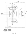
- the power saving control target circuit 103 may have a logic gate part 801 having two inputs as shown in FIG. 7 in place of the logic gate part 701 having one input as shown in FIG. 6 .
- the circuit shown in FIG. 7 can also function in the same way as the circuit shown in FIG. 6 and can realize the same effect as in the circuit shown in FIG. 6 .
- the power saving control target circuit 103 may include a logic gate part 903 , a source separating circuit 901 , and a source separating circuit 902 as shown in FIG. 8 .
- the logic gate part 903 functions as a logic gate part including a transistor generating high leak current
- the source separating circuit 901 controls the current supply from the high-potential side power supply
- the source separating circuit 902 controls the current supply from the low-potential side power supply.
- the conduction state of the transistor having a relatively large leak current is controlled by the Pch power saving mode signal and the Nch power saving mode signal.
- the conduction state of the transistor having a relatively large leak current is controlled by the PMOS transistor M 901 and the NMOS transistor M 902 of the source current separating circuit 901 by the Pch power saving mode signal and the Nch power saving mode signal.
- the leak current of the PMOS transistor M 903 is larger than that of the NMOS transistor M 904 in the configuration shown in FIG. 8 .
- the leak current of the PMOS transistor M 903 in the power saving control target circuit 103 is larger than that of the NMOS transistor M 904 as described above, the Pch power saving mode signal output from the P/N leak current comparator 101 is in the high level, and the Nch power saving mode signal is in the low level. Accordingly, the PMOS transistor M 901 of the source current separating circuit 901 is in the OFF state, and the NMOS transistor M 902 is in the ON state.
- the PMOS transistor M 901 Since the PMOS transistor M 901 is turned off, the current is disconnected regardless of whether the PMOS transistor M 903 of the logic gate part 903 is in the ON state or the OFF state. Since the NMOS transistor M 902 is in the ON state, the logic gate part 903 is connected to the low-potential side power supply. However, the PMOS transistor M 903 having a large leak current is not supplied with the current as described above, so that there is no influence on the pass-through current of the power saving control target circuit 103 .
- the leak current of the NMOS transistor M 904 is larger than that of the PMOS transistor M 903 , the PMOS transistor M 901 of the source current separating circuit 901 is in the ON state and the NMOS transistor M 902 is in the OFF state. Also in this case, the NMOS transistor M 904 having a large leak current is not supplied with the current; therefore there is no influence on the pass-through current of the power saving control target circuit 103 . As stated, also in this example, it is possible to effectively reduce the leak current of the circuit due to the variation of the manufacturing process.
- FIG. 9 shows a configuration example of a semiconductor integrated circuit 1000 according to the present embodiment.
- the difference between the first embodiment and the second embodiment is that there are a plurality of P/N leak current comparators 1011 and 1021 in the second embodiment and a plurality of sets of Pch and Nch power saving mode signals are input to the power saving control target circuit 1031 in accordance with characteristics of a plurality of transistors.
- two sets of Pch and Nch power saving mode signals are input to the power saving control target circuit 1031 by the two P/N leak current comparators 1011 and 1021 in the configuration shown in FIG. 9 , the number thereof is not limited.
- FIG. 10 shows a detailed circuit configuration of the power saving control target circuit 1031 shown in FIG. 9 .
- the transistor (or transistor group) having a gate whose ability of Pch is relatively high and the transistor (or transistor group) having a gate whose ability of Nch is relatively low are mixed in the power saving control target circuit 1031 , for example.
- FIG. 10 shows an example of the power saving control target circuit 1031 including two power saving control target circuits 103 (hereinafter referred to as circuit units 103 a and 103 b ) which are the same as shown in FIG. 6 .
- circuit units 103 a and 103 b are the same as shown in FIG. 6 .
- a case is assumed that the characteristics of the PMOS transistor and the NMOS transistor forming the logic gate parts 702 a and 702 b of the circuit units 103 a and 103 b are different. It is assumed here that the leak current of the PMOS transistor M 707 a in the logic gate part 702 a is larger than that of the NMOS transistor M 708 a and the leak current of the NMOS transistor M 708 b in the logic gate part 702 b is larger than that of the PMOS transistor M 707 b .
- the operation in the power saving mode will hereinafter be described according to its condition.
- the P/N leak current comparator 1011 includes transistors manufactured by the same process as that of the PMOS transistor M 707 a and the NMOS transistor M 708 a shown in FIG. 9 .
- the P/N leak current comparator 1021 includes transistors manufactured by the same process as that of the PMOS transistor M 707 b and the NMOS transistor M 708 b shown in FIG. 9 . Accordingly, the high-level leak current determination signal 1 and the low-level leak current determination signal 2 are output from the P/N leak current comparators 1011 and 1021 , respectively. These signals are the comparing result in accordance with the transistor characteristics included in the comparators.
- the leak current determination signal 1 and the leak current determination signal 2 are input to the P/N power saving mode signal generators 1012 and 1022 , respectively. Then a pair of the high-level Pch power saving mode signal 1 and the low-level Nch power saving mode signal 1 , and a pair of the low-level Pch power saving mode signal 2 and the high-level Nch power saving mode signal 2 are output to the circuit units 103 a and 103 b in the power saving control target circuit 1031 .
- the circuit unit 103 a in the power saving control target circuit 1031 receives the Pch power saving mode signal 1 and the Nch power saving mode signal 1 in accordance with the characteristic of the transistor as in the first embodiment so as to be operated.
- the circuit unit 103 b receives the Pch power saving mode signal 2 and the Nch power saving mode signal 2 in accordance with the characteristic of the transistor so as to be operated.
- the operation of each circuit unit 103 a and 103 b is the same as that in the above first embodiment, and the overlapping description thereof will be omitted.
- the leak current can be reduced more effectively by making the P/N leak current comparators 1011 and 1021 corresponding to each of the transistor characteristics correspondent to each other. Even when the different leak current is generated for each circuit unit 103 a and 103 b due to the temperature change or the like, the present invention can deal with this situation.
- the P/N leak current comparator may include resistors R 1201 , R 1202 , R 1203 , R 1204 for dividing the resistance, and a node F and a node G may be connected to different reference voltages.
- resistors R 1201 , R 1202 , R 1203 , R 1204 for dividing the resistance
- a node F and a node G may be connected to different reference voltages.
- the P/N leak current comparator 101 may have a configuration as shown in FIG. 12 .
- the P/N leak current comparator 101 includes a delay circuit 1301 , logic circuits 1302 and 1303 , and a latch circuit 1304 after the output terminal of the comparator 201 shown in FIG. 2 .
- the P/N leak current comparator 101 includes a function of preventing the output logical value of the leak current determination signal from being frequently switched when the leak current value of the PMOS transistor M 201 and the leak current value of the NMOS transistor M 202 are close to each other. The operation by the P/N leak current comparator 101 will now be described.
- the output of the comparator 201 changes from the high level to the low level in less than the predetermined delay time by the delay circuit 1301 .
- the output of the delay circuit 1301 remains the low level.
- the output of the logic circuit 1302 is made low level, and the output of the latch circuit 1304 remains the low level and does not change.
- the output of the latch circuit 1304 which is the output from the P/N leak current comparator 101 , does not change in a change where the output of the comparator 201 temporarily becomes high level.
- the output of the latch circuit 1304 is in the high level and the output of the comparator 201 changes from the high level to the low level.
- the output of the delay circuit 1301 changes from the high level to the low level if the output of the comparator 201 keeps the low-level state for more than a predetermined delay time by the delay circuit 1301 . Accordingly, both ends of the two input terminals of the logic circuit 1303 are in low level. Then the output of the logic circuit 1303 is also made high level and the output of the latch circuit 1304 changes to the low level.
- the output of the comparator 201 changes from the low level to the high level in less than the predetermined delay time by the delay circuit 1301 , the output of the delay circuit 1303 keeps the high level. Then the output of the logic circuit 1303 is made low level, and the output of the latch circuit 1304 keeps the high level and does not change.
- the output of the latch circuit 1304 which is the output from the P/N leak current comparator 101 , does not change in a change where the output of the comparator 201 temporarily becomes low level.
Landscapes
- Physics & Mathematics (AREA)
- Engineering & Computer Science (AREA)
- Computer Hardware Design (AREA)
- Computing Systems (AREA)
- General Engineering & Computer Science (AREA)
- Mathematical Physics (AREA)
- Semiconductor Integrated Circuits (AREA)
- Logic Circuits (AREA)
Abstract
Description
Claims (10)
Applications Claiming Priority (2)
| Application Number | Priority Date | Filing Date | Title |
|---|---|---|---|
| JP2007242012A JP5215622B2 (en) | 2007-09-19 | 2007-09-19 | Semiconductor integrated circuit and method for controlling semiconductor integrated circuit |
| JP2007-242012 | 2007-09-19 |
Publications (2)
| Publication Number | Publication Date |
|---|---|
| US20090072894A1 US20090072894A1 (en) | 2009-03-19 |
| US7719347B2 true US7719347B2 (en) | 2010-05-18 |
Family
ID=40453817
Family Applications (1)
| Application Number | Title | Priority Date | Filing Date |
|---|---|---|---|
| US12/230,907 Expired - Fee Related US7719347B2 (en) | 2007-09-19 | 2008-09-08 | Semiconductor integrated circuit and method of controlling the same |
Country Status (2)
| Country | Link |
|---|---|
| US (1) | US7719347B2 (en) |
| JP (1) | JP5215622B2 (en) |
Cited By (2)
| Publication number | Priority date | Publication date | Assignee | Title |
|---|---|---|---|---|
| US20100052770A1 (en) * | 2008-08-27 | 2010-03-04 | Kimiyoshi Usami | Power-off controlling circuit and power-off controlling method |
| US20100109764A1 (en) * | 2008-10-28 | 2010-05-06 | Lutz Dathe | Circuit, an adjusting method, and use of a control loop |
Families Citing this family (4)
| Publication number | Priority date | Publication date | Assignee | Title |
|---|---|---|---|---|
| US7760011B2 (en) * | 2007-08-10 | 2010-07-20 | Texas Instruments Incorporated | System and method for auto-power gating synthesis for active leakage reduction |
| JP2014093585A (en) * | 2012-11-01 | 2014-05-19 | Fujitsu Semiconductor Ltd | Semiconductor integrated circuit |
| US10620676B1 (en) | 2018-10-11 | 2020-04-14 | Analog Devices Global Unlimited Company | Wake-up control circuit for power-gated integrated circuits |
| US11545072B2 (en) * | 2021-06-08 | 2023-01-03 | Huizhou China Star Optoelectronics Display Co., Ltd. | Driving device of display panel and display device |
Citations (3)
| Publication number | Priority date | Publication date | Assignee | Title |
|---|---|---|---|---|
| US6087892A (en) * | 1998-06-08 | 2000-07-11 | Sun Microsystems, Inc. | Target Ion/Ioff threshold tuning circuit and method |
| JP2006012968A (en) | 2004-06-23 | 2006-01-12 | Nec Electronics Corp | Semiconductor integrated circuit device and design method thereof |
| US7425861B2 (en) * | 2005-06-29 | 2008-09-16 | Qimonda Ag | Device and method for regulating the threshold voltage of a transistor |
Family Cites Families (5)
| Publication number | Priority date | Publication date | Assignee | Title |
|---|---|---|---|---|
| JP4507121B2 (en) * | 1999-09-13 | 2010-07-21 | 株式会社ルネサステクノロジ | Semiconductor integrated circuit device |
| JP2002064150A (en) * | 2000-06-05 | 2002-02-28 | Mitsubishi Electric Corp | Semiconductor device |
| JP4184104B2 (en) * | 2003-01-30 | 2008-11-19 | 株式会社ルネサステクノロジ | Semiconductor device |
| JP4509765B2 (en) * | 2004-12-22 | 2010-07-21 | 株式会社東芝 | MOS type semiconductor integrated circuit device |
| WO2008129625A1 (en) * | 2007-04-10 | 2008-10-30 | Fujitsu Microelectronics Limited | Leak current detector circuit, body bias control circuit, semiconductor device, and semiconductor device testing method |
-
2007
- 2007-09-19 JP JP2007242012A patent/JP5215622B2/en not_active Expired - Fee Related
-
2008
- 2008-09-08 US US12/230,907 patent/US7719347B2/en not_active Expired - Fee Related
Patent Citations (4)
| Publication number | Priority date | Publication date | Assignee | Title |
|---|---|---|---|---|
| US6087892A (en) * | 1998-06-08 | 2000-07-11 | Sun Microsystems, Inc. | Target Ion/Ioff threshold tuning circuit and method |
| JP2006012968A (en) | 2004-06-23 | 2006-01-12 | Nec Electronics Corp | Semiconductor integrated circuit device and design method thereof |
| US7276956B2 (en) | 2004-06-23 | 2007-10-02 | Nec Electronics Corporation | Integrated circuit apparatus controlling source voltage of MOSFET based on temperature |
| US7425861B2 (en) * | 2005-06-29 | 2008-09-16 | Qimonda Ag | Device and method for regulating the threshold voltage of a transistor |
Cited By (5)
| Publication number | Priority date | Publication date | Assignee | Title |
|---|---|---|---|---|
| US20100052770A1 (en) * | 2008-08-27 | 2010-03-04 | Kimiyoshi Usami | Power-off controlling circuit and power-off controlling method |
| US7956678B2 (en) * | 2008-08-27 | 2011-06-07 | Shibaura Institute Of Technology | Power off controlling circuit and power-off controlling method |
| US20100109764A1 (en) * | 2008-10-28 | 2010-05-06 | Lutz Dathe | Circuit, an adjusting method, and use of a control loop |
| US8258860B2 (en) * | 2008-10-28 | 2012-09-04 | Atmel Corporation | Circuit, an adjusting method, and use of a control loop |
| US8525583B2 (en) | 2008-10-28 | 2013-09-03 | Atmel Corporation | Circuit, an adjusting method, and use of a control loop |
Also Published As
| Publication number | Publication date |
|---|---|
| US20090072894A1 (en) | 2009-03-19 |
| JP5215622B2 (en) | 2013-06-19 |
| JP2009076541A (en) | 2009-04-09 |
Similar Documents
| Publication | Publication Date | Title |
|---|---|---|
| KR100476725B1 (en) | Level shifter for detecting grounded power-supply and level shifting method | |
| US7719347B2 (en) | Semiconductor integrated circuit and method of controlling the same | |
| US6759876B2 (en) | Semiconductor integrated circuit | |
| US7332937B2 (en) | Dynamic logic with adaptive keeper | |
| US8018247B2 (en) | Apparatus and method for reducing power consumption using selective power gating | |
| US7109758B2 (en) | System and method for reducing short circuit current in a buffer | |
| US6566932B2 (en) | On-chip system with voltage level converting device for preventing leakage current due to voltage level difference | |
| JP3070373B2 (en) | Level shifter circuit | |
| KR20220031089A (en) | cross domain power control circuit | |
| US6340907B2 (en) | Schmitt trigger circuit having independent threshold voltage setting to provide hysteresis | |
| US7656210B2 (en) | Semiconductor integrated circuit | |
| US6604202B1 (en) | Low power processor | |
| US7804331B2 (en) | Semiconductor device | |
| JP7516332B2 (en) | Bus Buffer Circuit | |
| US20040263206A1 (en) | Pseudo-dynamic latch deracer | |
| JP3696194B2 (en) | Semiconductor integrated circuit | |
| JP2007329893A (en) | Apparatus and method for supplying voltage | |
| US6759877B1 (en) | Dynamic circuitry with on-chip temperature-controlled keeper device | |
| JP3807884B2 (en) | Low power information processing equipment | |
| JP3117404B2 (en) | Input circuit and semiconductor integrated circuit including the same | |
| Di et al. | Ultra-low power multi-threshold asynchronous circuit design | |
| JP4104634B2 (en) | Semiconductor device | |
| US6404238B1 (en) | Ratio logic gate with a current mirror | |
| JP2008219249A (en) | Cmos circuit | |
| JP2025152760A (en) | Semiconductor Devices |
Legal Events
| Date | Code | Title | Description |
|---|---|---|---|
| AS | Assignment |
Owner name: NEC ELECTRONICS CORPORATION, JAPAN Free format text: ASSIGNMENT OF ASSIGNORS INTEREST;ASSIGNOR:SUGIMOTO, HIDEKI;REEL/FRAME:021553/0822 Effective date: 20080826 Owner name: NEC ELECTRONICS CORPORATION,JAPAN Free format text: ASSIGNMENT OF ASSIGNORS INTEREST;ASSIGNOR:SUGIMOTO, HIDEKI;REEL/FRAME:021553/0822 Effective date: 20080826 |
|
| AS | Assignment |
Owner name: RENESAS ELECTRONICS CORPORATION, JAPAN Free format text: CHANGE OF NAME;ASSIGNOR:NEC ELECTRONICS CORPORATION;REEL/FRAME:025214/0687 Effective date: 20100401 |
|
| FEPP | Fee payment procedure |
Free format text: PAYOR NUMBER ASSIGNED (ORIGINAL EVENT CODE: ASPN); ENTITY STATUS OF PATENT OWNER: LARGE ENTITY |
|
| REMI | Maintenance fee reminder mailed | ||
| LAPS | Lapse for failure to pay maintenance fees | ||
| STCH | Information on status: patent discontinuation |
Free format text: PATENT EXPIRED DUE TO NONPAYMENT OF MAINTENANCE FEES UNDER 37 CFR 1.362 |
|
| STCH | Information on status: patent discontinuation |
Free format text: PATENT EXPIRED DUE TO NONPAYMENT OF MAINTENANCE FEES UNDER 37 CFR 1.362 |
|
| FP | Lapsed due to failure to pay maintenance fee |
Effective date: 20140518 |