US7717628B2 - System package using flexible optical and electrical wiring and signal processing method thereof - Google Patents
System package using flexible optical and electrical wiring and signal processing method thereof Download PDFInfo
- Publication number
- US7717628B2 US7717628B2 US12/350,978 US35097809A US7717628B2 US 7717628 B2 US7717628 B2 US 7717628B2 US 35097809 A US35097809 A US 35097809A US 7717628 B2 US7717628 B2 US 7717628B2
- Authority
- US
- United States
- Prior art keywords
- integrated circuit
- rigid substrates
- system package
- substrates
- flexible
- Prior art date
- Legal status (The legal status is an assumption and is not a legal conclusion. Google has not performed a legal analysis and makes no representation as to the accuracy of the status listed.)
- Active
Links
Images


Classifications
-
- G—PHYSICS
- G02—OPTICS
- G02B—OPTICAL ELEMENTS, SYSTEMS OR APPARATUS
- G02B6/00—Light guides; Structural details of arrangements comprising light guides and other optical elements, e.g. couplings
- G02B6/24—Coupling light guides
- G02B6/42—Coupling light guides with opto-electronic elements
- G02B6/43—Arrangements comprising a plurality of opto-electronic elements and associated optical interconnections
-
- H—ELECTRICITY
- H05—ELECTRIC TECHNIQUES NOT OTHERWISE PROVIDED FOR
- H05K—PRINTED CIRCUITS; CASINGS OR CONSTRUCTIONAL DETAILS OF ELECTRIC APPARATUS; MANUFACTURE OF ASSEMBLAGES OF ELECTRICAL COMPONENTS
- H05K1/00—Printed circuits
- H05K1/02—Details
- H05K1/0274—Optical details, e.g. printed circuits comprising integral optical means
-
- H10W40/22—
-
- H10W70/611—
-
- H10W70/688—
-
- H10W90/00—
-
- G—PHYSICS
- G02—OPTICS
- G02B—OPTICAL ELEMENTS, SYSTEMS OR APPARATUS
- G02B6/00—Light guides; Structural details of arrangements comprising light guides and other optical elements, e.g. couplings
- G02B6/24—Coupling light guides
- G02B6/42—Coupling light guides with opto-electronic elements
- G02B6/4201—Packages, e.g. shape, construction, internal or external details
- G02B6/4204—Packages, e.g. shape, construction, internal or external details the coupling comprising intermediate optical elements, e.g. lenses, holograms
- G02B6/4214—Packages, e.g. shape, construction, internal or external details the coupling comprising intermediate optical elements, e.g. lenses, holograms the intermediate optical element having redirecting reflective means, e.g. mirrors, prisms for deflecting the radiation from horizontal to down- or upward direction toward a device
-
- H—ELECTRICITY
- H05—ELECTRIC TECHNIQUES NOT OTHERWISE PROVIDED FOR
- H05K—PRINTED CIRCUITS; CASINGS OR CONSTRUCTIONAL DETAILS OF ELECTRIC APPARATUS; MANUFACTURE OF ASSEMBLAGES OF ELECTRICAL COMPONENTS
- H05K3/00—Apparatus or processes for manufacturing printed circuits
- H05K3/46—Manufacturing multilayer circuits
- H05K3/4688—Composite multilayer circuits, i.e. comprising insulating layers having different properties
- H05K3/4691—Rigid-flexible multilayer circuits comprising rigid and flexible layers, e.g. having in the bending regions only flexible layers
-
- H10W70/60—
-
- H10W70/63—
-
- H10W90/288—
-
- H10W90/724—
Definitions
- the present invention relates to a system package that uses flexible optical and electrical wiring, which connects two rigid substrates having at least one integrated circuit mounted thereon by using a flexible substrate with opto-electric wiring (optical waveguides and electrical wiring) and a signal processing method thereof.
- a system package technology utilizes a technology that forms a package with a multi-chip module formed of several chips, including highly integrated circuits, such as microprocessors in one package.
- RF IC radio-frequency integrated circuit
- Digital IC digital integrated circuit
- Analog IC analog integrated circuit
- Optical IC optical integrated circuit
- the system package is formed by mounting various integrated circuits on one substrate at high density, making it possible to reduce a size of the entire package, as well as perform various electrical functions.
- a system package using opto-electric wiring which can transmit electrical signals as well as optical signals by connecting a plurality of rigid substrates having a plurality of chips integrated thereon, and by using a flexible substrate that is optically and electrically wired and can be changed into various structures. Also, a signal processing method of the system package is provided.
- a system package using flexible opto-electric connections which can solve thermal problems by providing spacing between rigid substrates using a flexible substrate and can minimize electromagnetic wave interference that occurs when connecting high-speed data signals, by using the optical waveguides in the flexible substrate to effectively transmit data.
- a system package using flexible opto-electric wiring comprises a flexible substrate that can electrically and optically connect several rigid substrates having highly integrated electronic and opto-electric elements mounted thereon, and which can be easily bent, and which transmits signals without electromagnetic wave interference. Also, a signal processing method of the system package is disclosed.
- a system package using flexible opto-electric wiring including a plurality of rigid substrates having integrated circuit elements mounted thereon; a plurality of flexible substrates connected to the rigid substrates; and optical and electrical wires that are included in the rigid substrates and the flexible substrates to connect them to each other.
- the rigid substrates can be vertically stacked.
- the integrated circuit element includes an optical integrated circuit with a light source and a photo detector, a digital integrated circuit, an analog integrated circuit, and a high frequency integrated circuit.
- the system package further includes a heat dissipation device and/or an electromagnetic wave shielding device between the rigid substrates.
- a system package comprises at least one flexible substrate having an integrated circuit element mounted thereon and connected by optical and electrical wires.
- a signal processing method of a system package using flexible opto-electric wirings includes steps of applying data signals input by an external system to a first integrated circuit through electrical wires of a first rigid substrate, processing the signals by a processor of the first integrated circuit, and then converting the signals from electrical to optical form; transmitting the converted optical signals to a second rigid substrate via a flexible substrate; and converting the transmitted optical signals to electrical form through a second integrated circuit, processing the converted signals by the processor of the second integrated circuit, and then transmitting them to an external system.
- the external system comprises the flexible substrate, the external system board, and the rigid substrate.
- the system package is formed by connecting the plurality of rigid substrates using the flexible substrate that can be easily bent, it can be changed into various structures and easily installed without any structural limitation.
- the rigid substrates are electrically and optically connected by including opto-electric wiring (optical waveguides and electrical wiring) inside the flexible substrate, high-speed signal transmission can be achieved. Also, as the rigid substrates are formed by being spaced by a predetermined distance from each other, thermal problems caused by the integrated circuits is solved, which prevents the malfunction of the electronic processes.
- the electromagnetic wave interference problem caused due to the signal speed and the wire length is solved, such that errors in transmitting signals are prevented.
- the multi-process chip which can be operated at high-speed and has high reliability, is manufactured by mounting the plurality of processor chips (integrated circuits) in one integrated circuit system package, it can be variously applied to high-speed, high-reliability next generation electronic systems such as a next-generation computer.
- FIG. 1 is a cross-sectional view showing a system package of the prior art
- FIG. 2 is a cross-sectional view showing a system package using flexible opto-electric wiring according to one embodiment of the present invention
- FIGS. 3 and 4 are views showing a structure of a system package using bending properties of a flexible substrate according to one embodiment of the present invention
- FIG. 5 is a view showing a computer having a system package mounted therein according to one embodiment of the present invention
- FIG. 6 is a view showing a system package using flexible opto-electric wiring including an auxiliary device according to another embodiment of the present invention.
- FIG. 7 is a flow chart showing a signal processing method of an integrated circuit system package according to one embodiment of the present invention.
- a system package can be used by integrating a system on package (SOP), a system in package (SIP), and a multi-chip module (MCM).
- SOP system on package
- SIP system in package
- MCM multi-chip module
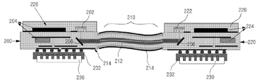
- FIG. 2 is a cross-sectional view showing a system package using flexible opto-electric wiring according to one embodiment of the present invention.
- the system package includes a first rigid substrate 200 , a flexible substrate 210 , and a second rigid substrate 220 .
- the rigid substrate can be made of thermosetting resin, ceramic, teflon and similar materials, for example, it can be made of thermosetting epoxy resin (FR-4) called by ‘prepreg’.
- the flexible substrate can be made of polyimide or similar materials.
- a point of reference between the rigidity and flexibility of the substrates is the possibility of substrate warpage. That is, the rigid substrate is not bent three-dimensionally after being hardened, except to a very minor extent.
- the flexible substrate is the sheet of film-type materials and is characteristic of three-dimensionally bent and curved substrate.
- the flexible substrate can be manufactured by the following process. First, optical waveguide sheets, comprised of the metal thin-film mirror tilted to the left or right, are laminated in the flexible substrate and electrically wired. Then the flexible substrate is inserted into the middle of the rigid substrate. The mechanical alignment or connection between the flexible substrate and the rigid substrate is made by using guide pins and holes (not shown in FIG. 2 ). On the other hand, the electrical connection between the flexible substrate and the rigid substrate is performed by via holes (not shown in FIG. 2 ).
- the first rigid substrate 200 and the second rigid substrate 220 include a light source 202 , a photo detector 222 , a first integrated circuit 204 , a second integrated circuit 224 , a mirror 206 , and a package cover 226 .
- the flexible substrate 210 includes an optical waveguide 212 and an electrical wire 214 .
- the first rigid substrate 200 and the second rigid substrate 220 are connected by using the flexible substrate 210 that can be easily bent, thereby forming the system package.
- the integrated circuit is formed on the flexible substrate, and the integrated circuit system package can be configured of only the flexible substrate. Further, one system package can be formed in a desired structure by using the plurality of rigid substrates 200 / 220 and the plurality of flexible substrates 210 .
- the first rigid substrate 200 includes a light source 202 that is an optical integrated element and comprises a first integrated circuit 204 that is configured of a digital integrated circuit, an analog integrated circuit, and a high frequency integrated circuit.
- the first integrated circuits 204 are mounted on the inside and outside of the first rigid substrate 200 and can be electrically connected through a system board 230 and an electric socket 232 that exist on the outside.
- the data signals input by the external system board 230 are applied to the first integrated circuits 204 through an internal electrical wire 214 in the first rigid substrate 200 and the data signals received in the first integrated circuit 204 are processed using the processor in the inside of the integrated circuit, electric-optic converted, and then transmitted to the optical waveguide 212 of the flexible substrate 210 via the light source 202 .
- the flexible substrate 210 comprises the electrical wire 214 and the optical waveguide 212 and the electrical wire 214 can be used for low-speed data transmission, a control signal line, a power supply line, and a ground line, and the like.
- the optical waveguide 212 can be used for high-speed data transmission, clock and control signal lines, and the like.
- the optical signal transmitted at high-speed through the optical waveguide 212 has no signal interference between the signal lines, unlike the high-speed electrical signals, making it possible to make the transmission length long.
- the second rigid substrate 220 receives the optical signals transmitted by the first rigid substrate 100 via the flexible substrate 210 through the photo detector 222 and the received signals are opto-electric-converted using the second integrated circuit 224 , processed according to the processor inside of the integrated circuit, and transmitted to the external system board 230 .
- a mirror 206 is installed inside of the first and second rigid substrates 200 and 220 at a predetermined angle (for example, 45°), thereby transmitting and receiving the signals without loss.
- the first and second integrated circuits 204 and 224 may be formed with various electronic elements such as capacitors, inductors, and resistors, and the like and the first and second integrated circuits 204 and 224 use a package cover 226 such that they can be protected from foreign materials such as dust.
- the package is formed in an order of the rigid substrate-flexible substrate-rigid substrate, but it is not particularly limited thereto. Therefore, the package may be formed of the rigid substrate having the integrated circuit mounted thereon and the flexible substrate having the integrated circuit mounted thereon or may be formed of only the flexible substrate having the integrated circuit mounted thereon.
- FIGS. 3 and 4 are a view showing the structure of the system package using the bending properties of the flexible substrate according to one embodiment of the present invention.
- FIG. 3 shows a vertically stacked system package
- FIG. 4 shows plane type of system package (i.e., formed on a plane).
- FIG. 5 is a view showing a computer having a system package mounted therein according to one embodiment of the present invention.
- a system package 400 can be effectively installed in a small space by using the flexible opto-electric wiring.
- the flexible opto-electric wiring comprises the optical waveguides and the electrical wires that are formed on the inside and outside of the flexible substrate that can be easily bent.
- FIG. 6 is a view showing a system package using flexible opto-electric wiring including an auxiliary device according to another embodiment of the present invention.
- the system package may comprise at least one auxiliary device 500 formed between the vertically stacked rigid substrates 300 as shown in FIG. 3 or FIG. 5 .
- the auxiliary device 500 is not particularly limited, but may comprise a heat dissipation device (heat sink) and an electromagnetic wave shielding device, and the like. According to the installation of the auxiliary device 500 , the errors in signals caused by the electromagnetic wave interference due to the heat and signals, which are generated by the integrated circuits 110 , 120 , 130 , and 140 are prevented, making it possible to accurately transmit data.
- heat sink heat dissipation device
- electromagnetic wave shielding device and the like.
- FIG. 7 is a flow chart showing the signal processing method of the integrated circuit system package according to another embodiment of the present invention.
- the high-speed data signals are applied from an external system board having the integrated circuit system package mounted thereon to the inside of the first rigid substrate via an electrical socket.
- step S 610 which includes electrical to optical conversion, the data signals applied to the inside of the first rigid substrate are processed through the first integrated circuit mounted on the rigid substrate via the wiring substrate and the processed electrical signals are converted into the optical signals.
- step S 620 which includes transmitting the signals, the converted optical signals are transmitted through the optical waveguides of the flexible substrate via the light source and transmitted to the photodetector of the second rigid substrate connected to the flexible substrate. At this time, the interference between the signals is minimized at the time of transmitting the data at high speed through the transmission of the optical signals, such that the data transmission length is not limited and the data can be transmitted up to a long distance.
- the optical signals received from the first rigid substrate are converted into the electrical signals in the second integrated circuit, processed through the processor of the second integrated circuit, and transmitted to the external system (S 640 ).
- the signals processed through the processor of the second integrated circuit can be transmitted to a third rigid substrate through the second flexible substrate or transmitted to the external system board having the second rigid substrate mounted thereon through the electrical socket.
- the electrical signals processed in the second rigid substrate are reversely subjected to the above processes and transmitted to the first rigid substrate, making it possible to process them in parallel with each other by using all the processors of the first integrated circuit and the second integrated circuit.
Landscapes
- Physics & Mathematics (AREA)
- Engineering & Computer Science (AREA)
- Microelectronics & Electronic Packaging (AREA)
- General Physics & Mathematics (AREA)
- Optics & Photonics (AREA)
- Structure Of Printed Boards (AREA)
- Light Receiving Elements (AREA)
Abstract
Description
Claims (7)
Applications Claiming Priority (2)
| Application Number | Priority Date | Filing Date | Title |
|---|---|---|---|
| KR1020080003925A KR20090078124A (en) | 2008-01-14 | 2008-01-14 | System Package and Flexible Signal Processing Method Using Flexible Photoelectric Wiring |
| KR10-2008-0003925 | 2008-01-14 |
Publications (2)
| Publication Number | Publication Date |
|---|---|
| US20090180733A1 US20090180733A1 (en) | 2009-07-16 |
| US7717628B2 true US7717628B2 (en) | 2010-05-18 |
Family
ID=40850702
Family Applications (1)
| Application Number | Title | Priority Date | Filing Date |
|---|---|---|---|
| US12/350,978 Active US7717628B2 (en) | 2008-01-14 | 2009-01-09 | System package using flexible optical and electrical wiring and signal processing method thereof |
Country Status (2)
| Country | Link |
|---|---|
| US (1) | US7717628B2 (en) |
| KR (1) | KR20090078124A (en) |
Cited By (6)
| Publication number | Priority date | Publication date | Assignee | Title |
|---|---|---|---|---|
| US20100195967A1 (en) * | 2009-02-02 | 2010-08-05 | Ibiden Co., Ltd. | Opto-electrical hybrid wiring board and method for manufacturing the same |
| US20110097034A1 (en) * | 2009-10-27 | 2011-04-28 | Kabushiki Kaisha Toshiba | Mounting structure |
| CN103560119A (en) * | 2013-11-05 | 2014-02-05 | 华进半导体封装先导技术研发中心有限公司 | Three-dimensional flexible substrate packaging structure used for multi-shield chips and three-dimensional flexible substrate manufacturing method |
| CN103745959A (en) * | 2014-01-09 | 2014-04-23 | 华进半导体封装先导技术研发中心有限公司 | Three-dimension system packaging structure based on rigid-flexible combined printed circuit board |
| US20180364071A1 (en) * | 2017-06-16 | 2018-12-20 | Daniel Rivera | Photonic computer system comprised of stack disk arrays running on but not limited to quantum software |
| US10459160B2 (en) | 2017-01-31 | 2019-10-29 | Corning Optical Communications LLC | Glass waveguide assemblies for OE-PCBs and methods of forming OE-PCBs |
Families Citing this family (14)
| Publication number | Priority date | Publication date | Assignee | Title |
|---|---|---|---|---|
| US7885494B2 (en) * | 2008-07-02 | 2011-02-08 | Sony Ericsson Mobile Communications Ab | Optical signaling for a package-on-package stack |
| JP2013167750A (en) * | 2012-02-15 | 2013-08-29 | Hitachi Cable Ltd | Photoelectric composite wiring module |
| CN103762203B (en) * | 2014-01-09 | 2016-08-24 | 华进半导体封装先导技术研发中心有限公司 | Radiator structure based on rigid flexible system printed circuit board (PCB) three-dimension packaging and preparation method |
| CN103763848B (en) * | 2014-01-09 | 2017-01-25 | 华进半导体封装先导技术研发中心有限公司 | Mixed signal system three-dimensional packaging structure based on digital-analog mixture requirements and manufacturing method |
| CN104900611B (en) * | 2015-06-09 | 2017-09-08 | 中国科学院微电子研究所 | Three-dimensional packaging heat dissipation structure based on flexible substrate and its preparation method |
| US20160377356A1 (en) * | 2015-06-25 | 2016-12-29 | Asia Vital Components Co., Ltd. | Flexible and transformable water-cooling device |
| WO2017099730A1 (en) * | 2015-12-08 | 2017-06-15 | Intel Corporation | Wireless interconnects on flexible cables between computing platforms |
| US10094788B2 (en) * | 2015-12-21 | 2018-10-09 | Applied Materials, Inc. | Surface acoustic wave sensors in semiconductor processing equipment |
| US9633950B1 (en) * | 2016-02-10 | 2017-04-25 | Qualcomm Incorporated | Integrated device comprising flexible connector between integrated circuit (IC) packages |
| KR102628512B1 (en) * | 2016-07-14 | 2024-01-25 | 삼성전자주식회사 | Electronic device |
| US10912204B2 (en) | 2018-03-30 | 2021-02-02 | Samsung Electro-Mechanics Co., Ltd. | Electronic device and rigid-flexible substrate module |
| US10638616B1 (en) * | 2018-10-30 | 2020-04-28 | Taiwan Semiconductor Manufacturing Co., Ltd. | Circuit carrier and manifacturing method thereof |
| CN115706104A (en) * | 2021-08-13 | 2023-02-17 | 华为技术有限公司 | On-board optical interconnection device and communication equipment |
| CN119252809B (en) * | 2024-09-29 | 2025-06-13 | 南通大学 | A novel three-dimensional packaging structure based on flexible substrate and chip heat dissipation method |
Citations (7)
| Publication number | Priority date | Publication date | Assignee | Title |
|---|---|---|---|---|
| US5757998A (en) * | 1996-10-02 | 1998-05-26 | International Business Machines Corporation | Multigigabit adaptable transceiver module |
| US6611635B1 (en) * | 1998-10-09 | 2003-08-26 | Fujitsu Limited | Opto-electronic substrates with electrical and optical interconnections and methods for making |
| US20040218848A1 (en) * | 2003-04-30 | 2004-11-04 | Industrial Technology Research Institute | Flexible electronic/optical interconnection film assembly and method for manufacturing |
| US20070019914A1 (en) * | 2005-07-25 | 2007-01-25 | Fuji Xerox Co., Ltd. | Optical waveguide film, and light transmission and reception module |
| US7333682B2 (en) * | 2004-09-22 | 2008-02-19 | Hitachi Cable, Ltd. | Photoelectric composite interconnection assembly and electronics device using same |
| US20080075405A1 (en) * | 2006-09-19 | 2008-03-27 | Ibiden Co., Ltd | Optical interconnect device and method for manufacturing the same |
| US7509001B2 (en) * | 2006-12-21 | 2009-03-24 | Hitachi Cable Ltd. | Optical circuit board |
-
2008
- 2008-01-14 KR KR1020080003925A patent/KR20090078124A/en not_active Ceased
-
2009
- 2009-01-09 US US12/350,978 patent/US7717628B2/en active Active
Patent Citations (7)
| Publication number | Priority date | Publication date | Assignee | Title |
|---|---|---|---|---|
| US5757998A (en) * | 1996-10-02 | 1998-05-26 | International Business Machines Corporation | Multigigabit adaptable transceiver module |
| US6611635B1 (en) * | 1998-10-09 | 2003-08-26 | Fujitsu Limited | Opto-electronic substrates with electrical and optical interconnections and methods for making |
| US20040218848A1 (en) * | 2003-04-30 | 2004-11-04 | Industrial Technology Research Institute | Flexible electronic/optical interconnection film assembly and method for manufacturing |
| US7333682B2 (en) * | 2004-09-22 | 2008-02-19 | Hitachi Cable, Ltd. | Photoelectric composite interconnection assembly and electronics device using same |
| US20070019914A1 (en) * | 2005-07-25 | 2007-01-25 | Fuji Xerox Co., Ltd. | Optical waveguide film, and light transmission and reception module |
| US20080075405A1 (en) * | 2006-09-19 | 2008-03-27 | Ibiden Co., Ltd | Optical interconnect device and method for manufacturing the same |
| US7509001B2 (en) * | 2006-12-21 | 2009-03-24 | Hitachi Cable Ltd. | Optical circuit board |
Cited By (10)
| Publication number | Priority date | Publication date | Assignee | Title |
|---|---|---|---|---|
| US20100195967A1 (en) * | 2009-02-02 | 2010-08-05 | Ibiden Co., Ltd. | Opto-electrical hybrid wiring board and method for manufacturing the same |
| US8275223B2 (en) * | 2009-02-02 | 2012-09-25 | Ibiden Co., Ltd. | Opto-electrical hybrid wiring board and method for manufacturing the same |
| US8340480B2 (en) | 2009-02-02 | 2012-12-25 | Ibiden Co., Ltd. | Opto-electrical hybrid wiring board and method for manufacturing the same |
| US20110097034A1 (en) * | 2009-10-27 | 2011-04-28 | Kabushiki Kaisha Toshiba | Mounting structure |
| US8380022B2 (en) * | 2009-10-27 | 2013-02-19 | Kabushiki Kaisha Toshiba | Mounting structure |
| CN103560119A (en) * | 2013-11-05 | 2014-02-05 | 华进半导体封装先导技术研发中心有限公司 | Three-dimensional flexible substrate packaging structure used for multi-shield chips and three-dimensional flexible substrate manufacturing method |
| CN103560119B (en) * | 2013-11-05 | 2016-06-01 | 华进半导体封装先导技术研发中心有限公司 | For shielding three-dimension flexible substrate encapsulation structure and the making method of chip more |
| CN103745959A (en) * | 2014-01-09 | 2014-04-23 | 华进半导体封装先导技术研发中心有限公司 | Three-dimension system packaging structure based on rigid-flexible combined printed circuit board |
| US10459160B2 (en) | 2017-01-31 | 2019-10-29 | Corning Optical Communications LLC | Glass waveguide assemblies for OE-PCBs and methods of forming OE-PCBs |
| US20180364071A1 (en) * | 2017-06-16 | 2018-12-20 | Daniel Rivera | Photonic computer system comprised of stack disk arrays running on but not limited to quantum software |
Also Published As
| Publication number | Publication date |
|---|---|
| US20090180733A1 (en) | 2009-07-16 |
| KR20090078124A (en) | 2009-07-17 |
Similar Documents
| Publication | Publication Date | Title |
|---|---|---|
| US7717628B2 (en) | System package using flexible optical and electrical wiring and signal processing method thereof | |
| US7470069B1 (en) | Optoelectronic MCM package | |
| CN104011856B (en) | Film interpolater for IC apparatus | |
| US7215845B1 (en) | Optical interconnect architecture | |
| KR100911508B1 (en) | Photoelectric integrated circuit device and transmission device using same | |
| US6685364B1 (en) | Enhanced folded flexible cable packaging for use in optical transceivers | |
| US20210014965A1 (en) | Hybrid carrier board and manufacturing method, assembly, and optical module thereof | |
| US20090032921A1 (en) | Printed wiring board structure and electronic apparatus | |
| US10332937B2 (en) | Semiconductor device having a protruding interposer edge face | |
| US8164917B2 (en) | Base plate for use in a multi-chip module | |
| US20080078571A1 (en) | Device mounting board and semiconductor module | |
| US9523830B2 (en) | Optical module and transmitting device | |
| US10020249B2 (en) | Electronic device package using a substrate side coaxial interface | |
| JP2007293018A (en) | Photoelectric composite module and optical input / output device | |
| TWI262582B (en) | LSI package, circuit device including the same, and manufacturing method of circuit device | |
| WO2007088959A1 (en) | Optical module | |
| JP2004063861A (en) | Optical communication apparatus, optical transmitter, optical transceiver, and optical transmission system | |
| JP4630409B2 (en) | Optoelectronic integrated circuit device | |
| US7249896B2 (en) | Array optical sub-assembly | |
| JP2004235636A (en) | Integrated VCSEL on ASIC module using flexible electrical connections | |
| US6659656B2 (en) | Packaging architecture for a multiple array transceiver using a winged flexible cable for optimal wiring | |
| US20110091168A1 (en) | Opto-electrical assemblies and associated apparatus and methods | |
| KR20100095185A (en) | All-in-one embedded connection module | |
| CN102573374A (en) | Electronic apparatus, method for mounting a device, and optical communication apparatus | |
| WO2010131578A1 (en) | Semiconductor device with built-in optical signal input and output device and electronic device equipped with same |
Legal Events
| Date | Code | Title | Description |
|---|---|---|---|
| AS | Assignment |
Owner name: KOREA PHOTONICS TECHNOLOGY INSTITUTE, KOREA, REPUB Free format text: ASSIGNMENT OF ASSIGNORS INTEREST;ASSIGNORS:HWANG, SUNG HWAN;RHO, BYUNG SUP;LIM, JUNG WOON;AND OTHERS;REEL/FRAME:022080/0638 Effective date: 20090108 Owner name: KOREA PHOTONICS TECHNOLOGY INSTITUTE,KOREA, REPUBL Free format text: ASSIGNMENT OF ASSIGNORS INTEREST;ASSIGNORS:HWANG, SUNG HWAN;RHO, BYUNG SUP;LIM, JUNG WOON;AND OTHERS;REEL/FRAME:022080/0638 Effective date: 20090108 |
|
| STCF | Information on status: patent grant |
Free format text: PATENTED CASE |
|
| FPAY | Fee payment |
Year of fee payment: 4 |
|
| MAFP | Maintenance fee payment |
Free format text: PAYMENT OF MAINTENANCE FEE, 8TH YR, SMALL ENTITY (ORIGINAL EVENT CODE: M2552) Year of fee payment: 8 |
|
| MAFP | Maintenance fee payment |
Free format text: PAYMENT OF MAINTENANCE FEE, 12TH YR, SMALL ENTITY (ORIGINAL EVENT CODE: M2553); ENTITY STATUS OF PATENT OWNER: SMALL ENTITY Year of fee payment: 12 |