US7715726B2 - High immunity clock regeneration over optically isolated channel - Google Patents
High immunity clock regeneration over optically isolated channel Download PDFInfo
- Publication number
- US7715726B2 US7715726B2 US11/751,389 US75138907A US7715726B2 US 7715726 B2 US7715726 B2 US 7715726B2 US 75138907 A US75138907 A US 75138907A US 7715726 B2 US7715726 B2 US 7715726B2
- Authority
- US
- United States
- Prior art keywords
- circuit
- clock signal
- opto
- isolator
- input
- Prior art date
- Legal status (The legal status is an assumption and is not a legal conclusion. Google has not performed a legal analysis and makes no representation as to the accuracy of the status listed.)
- Expired - Fee Related, expires
Links
Images


Classifications
-
- H—ELECTRICITY
- H03—ELECTRONIC CIRCUITRY
- H03M—CODING; DECODING; CODE CONVERSION IN GENERAL
- H03M1/00—Analogue/digital conversion; Digital/analogue conversion
- H03M1/06—Continuously compensating for, or preventing, undesired influence of physical parameters
- H03M1/08—Continuously compensating for, or preventing, undesired influence of physical parameters of noise
- H03M1/0827—Continuously compensating for, or preventing, undesired influence of physical parameters of noise of electromagnetic or electrostatic field noise, e.g. preventing crosstalk by shielding or optical isolation
-
- H—ELECTRICITY
- H03—ELECTRONIC CIRCUITRY
- H03M—CODING; DECODING; CODE CONVERSION IN GENERAL
- H03M3/00—Conversion of analogue values to or from differential modulation
- H03M3/30—Delta-sigma modulation
- H03M3/322—Continuously compensating for, or preventing, undesired influence of physical parameters
- H03M3/368—Continuously compensating for, or preventing, undesired influence of physical parameters of noise other than the quantisation noise already being shaped inherently by delta-sigma modulators
-
- H—ELECTRICITY
- H03—ELECTRONIC CIRCUITRY
- H03M—CODING; DECODING; CODE CONVERSION IN GENERAL
- H03M1/00—Analogue/digital conversion; Digital/analogue conversion
- H03M1/12—Analogue/digital converters
-
- H—ELECTRICITY
- H03—ELECTRONIC CIRCUITRY
- H03M—CODING; DECODING; CODE CONVERSION IN GENERAL
- H03M3/00—Conversion of analogue values to or from differential modulation
- H03M3/30—Delta-sigma modulation
- H03M3/458—Analogue/digital converters using delta-sigma modulation as an intermediate step
Definitions
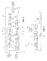
- ADC 68 operates in the conventional manner, converting an analog input signal, such as a signal received from a motor voltage or current sensing circuit, to a digital output signal.
- Sigma-delta ADCs are sensitive to clock jitter and operate best when the clock signal has a duty cycle of exactly 50 percent.
- the clock signal synthesized by PLL 66 has a very precise 50 percent duty cycle, even if the signal that is input to PLL 66 does not have a 50 percent duty cycle.
- the inherent low-pass characteristic of PLL 66 both filters out any clock jitter that may occur due to electrical or optical imperfections in the optically isolated clock channel defined by opto-isolator 48 and rejects any high-frequency voltage spikes that may be transmitted across the channel.
Landscapes
- Engineering & Computer Science (AREA)
- Theoretical Computer Science (AREA)
- Physics & Mathematics (AREA)
- Electromagnetism (AREA)
- Stabilization Of Oscillater, Synchronisation, Frequency Synthesizers (AREA)
- Compression, Expansion, Code Conversion, And Decoders (AREA)
- Electronic Switches (AREA)
Abstract
Description
Claims (14)
Priority Applications (2)
| Application Number | Priority Date | Filing Date | Title |
|---|---|---|---|
| US11/751,389 US7715726B2 (en) | 2007-05-21 | 2007-05-21 | High immunity clock regeneration over optically isolated channel |
| JP2008133243A JP2009081829A (en) | 2007-05-21 | 2008-05-21 | High immunity clock regeneration over optically isolated channel |
Applications Claiming Priority (1)
| Application Number | Priority Date | Filing Date | Title |
|---|---|---|---|
| US11/751,389 US7715726B2 (en) | 2007-05-21 | 2007-05-21 | High immunity clock regeneration over optically isolated channel |
Publications (2)
| Publication Number | Publication Date |
|---|---|
| US20080292325A1 US20080292325A1 (en) | 2008-11-27 |
| US7715726B2 true US7715726B2 (en) | 2010-05-11 |
Family
ID=40072510
Family Applications (1)
| Application Number | Title | Priority Date | Filing Date |
|---|---|---|---|
| US11/751,389 Expired - Fee Related US7715726B2 (en) | 2007-05-21 | 2007-05-21 | High immunity clock regeneration over optically isolated channel |
Country Status (2)
| Country | Link |
|---|---|
| US (1) | US7715726B2 (en) |
| JP (1) | JP2009081829A (en) |
Cited By (4)
| Publication number | Priority date | Publication date | Assignee | Title |
|---|---|---|---|---|
| US20120018615A1 (en) * | 2010-07-22 | 2012-01-26 | Azad Siahmakoun | Photonic second-order delta-sigma modulator |
| US10389434B1 (en) * | 2018-11-06 | 2019-08-20 | Analog Devices, Inc. | Bi-directional data isolator with dynamic communication |
| US11246200B2 (en) * | 2019-09-19 | 2022-02-08 | Kabushiki Kaisha Toshiba | LED drive control circuitry, electronic circuitry, and LED drive control method |
| US12050487B2 (en) * | 2022-03-18 | 2024-07-30 | Kabushiki Kaisha Toshiba | Electronic circuitry |
Families Citing this family (8)
| Publication number | Priority date | Publication date | Assignee | Title |
|---|---|---|---|---|
| US8116055B2 (en) * | 2007-06-21 | 2012-02-14 | Avago Technologies Ecbu Ip (Singapore) Pte. Ltd. | Methods and apparatuses for performing common mode pulse compensation in an opto-isolator |
| US7808759B2 (en) * | 2007-06-21 | 2010-10-05 | Avago Technologies Ecbu Ip (Singapore) Pte. Ltd. | Methods and apparatuses for performing common mode pulse compensation in an opto-isolator |
| MX2013002476A (en) * | 2010-09-13 | 2013-06-11 | Micro Motion Inc | Opto-isolation circuit. |
| DE102012112234A1 (en) * | 2012-12-13 | 2014-06-18 | Endress + Hauser Gmbh + Co. Kg | Device for synchronizing clock frequencies |
| US9479325B1 (en) * | 2013-04-12 | 2016-10-25 | Maxim Integrated Products, Inc. | Reduced frequency backwards clock for isolated sigma-delta modulators |
| EP3573236A4 (en) * | 2017-01-18 | 2020-01-22 | Mitsubishi Electric Corporation | ISOLATOR CIRCUIT |
| JP2024002555A (en) * | 2022-06-24 | 2024-01-11 | ローム株式会社 | signal transmission device |
| CN116561038A (en) * | 2023-04-26 | 2023-08-08 | 深圳市锐能微科技有限公司 | Serial communication method, device, serial communication system and medium |
Citations (1)
| Publication number | Priority date | Publication date | Assignee | Title |
|---|---|---|---|---|
| US20040041947A1 (en) * | 2002-08-29 | 2004-03-04 | Lsi Logic Corporation | Frequency controller |
Family Cites Families (9)
| Publication number | Priority date | Publication date | Assignee | Title |
|---|---|---|---|---|
| JPS63246918A (en) * | 1987-04-01 | 1988-10-13 | Nec Corp | Polyphase clock generating circuit |
| JPS63292820A (en) * | 1987-05-26 | 1988-11-30 | Matsushita Electric Works Ltd | Pulse generation circuit |
| JPH06284155A (en) * | 1992-11-25 | 1994-10-07 | Yamaha Corp | Modulator and demodulator |
| JP3277038B2 (en) * | 1993-08-05 | 2002-04-22 | シャープ株式会社 | Optical transmission equipment |
| JP3968770B2 (en) * | 2001-05-02 | 2007-08-29 | 富士ゼロックス株式会社 | Signal transmission system and apparatus |
| JP4045754B2 (en) * | 2001-05-07 | 2008-02-13 | 富士ゼロックス株式会社 | Optical transmission system and apparatus |
| JP4871458B2 (en) * | 2001-06-13 | 2012-02-08 | 株式会社高見沢サイバネティックス | Data conversion device and telemeter device |
| JP2006157849A (en) * | 2004-10-26 | 2006-06-15 | Seiko Epson Corp | Frequency divider circuit and semiconductor integrated circuit having the same |
| JP4805746B2 (en) * | 2006-07-27 | 2011-11-02 | 株式会社山武 | ΔΣ A / D converter |
-
2007
- 2007-05-21 US US11/751,389 patent/US7715726B2/en not_active Expired - Fee Related
-
2008
- 2008-05-21 JP JP2008133243A patent/JP2009081829A/en active Pending
Patent Citations (1)
| Publication number | Priority date | Publication date | Assignee | Title |
|---|---|---|---|---|
| US20040041947A1 (en) * | 2002-08-29 | 2004-03-04 | Lsi Logic Corporation | Frequency controller |
Cited By (7)
| Publication number | Priority date | Publication date | Assignee | Title |
|---|---|---|---|---|
| US20120018615A1 (en) * | 2010-07-22 | 2012-01-26 | Azad Siahmakoun | Photonic second-order delta-sigma modulator |
| US10389434B1 (en) * | 2018-11-06 | 2019-08-20 | Analog Devices, Inc. | Bi-directional data isolator with dynamic communication |
| US10659150B1 (en) * | 2018-11-06 | 2020-05-19 | Analog Devices, Inc. | Bi-directional data isolator with dynamic communication |
| US11246200B2 (en) * | 2019-09-19 | 2022-02-08 | Kabushiki Kaisha Toshiba | LED drive control circuitry, electronic circuitry, and LED drive control method |
| US20220117055A1 (en) * | 2019-09-19 | 2022-04-14 | Kabushiki Kaisha Toshiba | Led drive control circuitry, electronic circuitry, and led drive control method |
| US11706854B2 (en) * | 2019-09-19 | 2023-07-18 | Kabushiki Kaisha Toshiba | LED drive control circuitry, electronic circuitry, and LED drive control method |
| US12050487B2 (en) * | 2022-03-18 | 2024-07-30 | Kabushiki Kaisha Toshiba | Electronic circuitry |
Also Published As
| Publication number | Publication date |
|---|---|
| US20080292325A1 (en) | 2008-11-27 |
| JP2009081829A (en) | 2009-04-16 |
Similar Documents
| Publication | Publication Date | Title |
|---|---|---|
| US7715726B2 (en) | High immunity clock regeneration over optically isolated channel | |
| US8368441B2 (en) | Semiconductor integrated circuit having an on-chip PLL and operating method thereof | |
| US6041090A (en) | Data sampling and recover in a phase-locked loop (PLL) | |
| JP5102603B2 (en) | Semiconductor integrated circuit | |
| US7710304B2 (en) | A/D converter and semiconductor device | |
| US8405465B2 (en) | Duty cycle translator methods and apparatus | |
| CN104113303B (en) | 50% duty ratio clock generation circuit | |
| US9425781B2 (en) | Syncless unit interval variation tolerant PWM receiver circuit, system and method | |
| CN101997629A (en) | Transceiver and operating method thereof | |
| US20060214712A1 (en) | Digital pulse width modulator | |
| US20090128198A1 (en) | Digital frequency synthesizer | |
| JP5959422B2 (en) | Clock recovery circuit, light receiving circuit, optical coupling device, and frequency synthesizer | |
| CN110365331B (en) | A lock detection device for integrated phase-locked loop | |
| US7826578B1 (en) | Circuits and methods for noise management in systems including an asynchronously-operable data port | |
| JP2013009083A (en) | A/d converter | |
| US11706854B2 (en) | LED drive control circuitry, electronic circuitry, and LED drive control method | |
| US8396112B2 (en) | Circuitry and method for transferring data, and circuitry and method utilizing clock pulses | |
| US7567641B2 (en) | Sample rate conversion systems with an independent internal oscillator | |
| US10698439B1 (en) | Efficient clock forwarding scheme | |
| CN113900478A (en) | Clock module design method suitable for SoC chip | |
| JP5642615B2 (en) | Oscillator | |
| JP2003121506A5 (en) | ||
| CN1198271A (en) | PLL | |
| CN213365516U (en) | Interface conversion circuit and interface conversion device | |
| CN101507115B (en) | Semiconductor device and system and method of crystal sharing |
Legal Events
| Date | Code | Title | Description |
|---|---|---|---|
| AS | Assignment |
Owner name: AVAGO TECHNOLOGIES ECBU IP (SINGAPORE) PTE. LTD., Free format text: ASSIGNMENT OF ASSIGNORS INTEREST;ASSIGNORS:CHEN, LEI;CHOW, FUN KOK;REEL/FRAME:020515/0641 Effective date: 20070518 Owner name: AVAGO TECHNOLOGIES ECBU IP (SINGAPORE) PTE. LTD.,S Free format text: ASSIGNMENT OF ASSIGNORS INTEREST;ASSIGNORS:CHEN, LEI;CHOW, FUN KOK;REEL/FRAME:020515/0641 Effective date: 20070518 |
|
| STCF | Information on status: patent grant |
Free format text: PATENTED CASE |
|
| AS | Assignment |
Owner name: AVAGO TECHNOLOGIES GENERAL IP (SINGAPORE) PTE. LTD., SINGAPORE Free format text: MERGER;ASSIGNOR:AVAGO TECHNOLOGIES ECBU IP (SINGAPORE) PTE. LTD.;REEL/FRAME:030369/0528 Effective date: 20121030 Owner name: AVAGO TECHNOLOGIES GENERAL IP (SINGAPORE) PTE. LTD Free format text: MERGER;ASSIGNOR:AVAGO TECHNOLOGIES ECBU IP (SINGAPORE) PTE. LTD.;REEL/FRAME:030369/0528 Effective date: 20121030 |
|
| FPAY | Fee payment |
Year of fee payment: 4 |
|
| AS | Assignment |
Owner name: DEUTSCHE BANK AG NEW YORK BRANCH, AS COLLATERAL AGENT, NEW YORK Free format text: PATENT SECURITY AGREEMENT;ASSIGNOR:AVAGO TECHNOLOGIES GENERAL IP (SINGAPORE) PTE. LTD.;REEL/FRAME:032851/0001 Effective date: 20140506 Owner name: DEUTSCHE BANK AG NEW YORK BRANCH, AS COLLATERAL AG Free format text: PATENT SECURITY AGREEMENT;ASSIGNOR:AVAGO TECHNOLOGIES GENERAL IP (SINGAPORE) PTE. LTD.;REEL/FRAME:032851/0001 Effective date: 20140506 |
|
| AS | Assignment |
Owner name: AVAGO TECHNOLOGIES GENERAL IP (SINGAPORE) PTE. LTD., SINGAPORE Free format text: TERMINATION AND RELEASE OF SECURITY INTEREST IN PATENT RIGHTS (RELEASES RF 032851-0001);ASSIGNOR:DEUTSCHE BANK AG NEW YORK BRANCH, AS COLLATERAL AGENT;REEL/FRAME:037689/0001 Effective date: 20160201 Owner name: AVAGO TECHNOLOGIES GENERAL IP (SINGAPORE) PTE. LTD Free format text: TERMINATION AND RELEASE OF SECURITY INTEREST IN PATENT RIGHTS (RELEASES RF 032851-0001);ASSIGNOR:DEUTSCHE BANK AG NEW YORK BRANCH, AS COLLATERAL AGENT;REEL/FRAME:037689/0001 Effective date: 20160201 |
|
| AS | Assignment |
Owner name: BANK OF AMERICA, N.A., AS COLLATERAL AGENT, NORTH CAROLINA Free format text: PATENT SECURITY AGREEMENT;ASSIGNOR:AVAGO TECHNOLOGIES GENERAL IP (SINGAPORE) PTE. LTD.;REEL/FRAME:037808/0001 Effective date: 20160201 Owner name: BANK OF AMERICA, N.A., AS COLLATERAL AGENT, NORTH Free format text: PATENT SECURITY AGREEMENT;ASSIGNOR:AVAGO TECHNOLOGIES GENERAL IP (SINGAPORE) PTE. LTD.;REEL/FRAME:037808/0001 Effective date: 20160201 |
|
| AS | Assignment |
Owner name: AVAGO TECHNOLOGIES GENERAL IP (SINGAPORE) PTE. LTD., SINGAPORE Free format text: TERMINATION AND RELEASE OF SECURITY INTEREST IN PATENTS;ASSIGNOR:BANK OF AMERICA, N.A., AS COLLATERAL AGENT;REEL/FRAME:041710/0001 Effective date: 20170119 Owner name: AVAGO TECHNOLOGIES GENERAL IP (SINGAPORE) PTE. LTD Free format text: TERMINATION AND RELEASE OF SECURITY INTEREST IN PATENTS;ASSIGNOR:BANK OF AMERICA, N.A., AS COLLATERAL AGENT;REEL/FRAME:041710/0001 Effective date: 20170119 |
|
| MAFP | Maintenance fee payment |
Free format text: PAYMENT OF MAINTENANCE FEE, 8TH YEAR, LARGE ENTITY (ORIGINAL EVENT CODE: M1552) Year of fee payment: 8 |
|
| AS | Assignment |
Owner name: AVAGO TECHNOLOGIES INTERNATIONAL SALES PTE. LIMITED, SINGAPORE Free format text: MERGER;ASSIGNOR:AVAGO TECHNOLOGIES GENERAL IP (SINGAPORE) PTE. LTD.;REEL/FRAME:047196/0687 Effective date: 20180509 Owner name: AVAGO TECHNOLOGIES INTERNATIONAL SALES PTE. LIMITE Free format text: MERGER;ASSIGNOR:AVAGO TECHNOLOGIES GENERAL IP (SINGAPORE) PTE. LTD.;REEL/FRAME:047196/0687 Effective date: 20180509 |
|
| AS | Assignment |
Owner name: AVAGO TECHNOLOGIES INTERNATIONAL SALES PTE. LIMITED, SINGAPORE Free format text: CORRECTIVE ASSIGNMENT TO CORRECT THE EFFECTIVE DATE OF MERGER TO 9/5/2018 PREVIOUSLY RECORDED AT REEL: 047196 FRAME: 0687. ASSIGNOR(S) HEREBY CONFIRMS THE MERGER;ASSIGNOR:AVAGO TECHNOLOGIES GENERAL IP (SINGAPORE) PTE. LTD.;REEL/FRAME:047630/0344 Effective date: 20180905 Owner name: AVAGO TECHNOLOGIES INTERNATIONAL SALES PTE. LIMITE Free format text: CORRECTIVE ASSIGNMENT TO CORRECT THE EFFECTIVE DATE OF MERGER TO 9/5/2018 PREVIOUSLY RECORDED AT REEL: 047196 FRAME: 0687. ASSIGNOR(S) HEREBY CONFIRMS THE MERGER;ASSIGNOR:AVAGO TECHNOLOGIES GENERAL IP (SINGAPORE) PTE. LTD.;REEL/FRAME:047630/0344 Effective date: 20180905 |
|
| AS | Assignment |
Owner name: AVAGO TECHNOLOGIES INTERNATIONAL SALES PTE. LIMITE Free format text: CORRECTIVE ASSIGNMENT TO CORRECT THE PROPERTY NUMBERS PREVIOUSLY RECORDED AT REEL: 47630 FRAME: 344. ASSIGNOR(S) HEREBY CONFIRMS THE ASSIGNMENT;ASSIGNOR:AVAGO TECHNOLOGIES GENERAL IP (SINGAPORE) PTE. LTD.;REEL/FRAME:048883/0267 Effective date: 20180905 Owner name: AVAGO TECHNOLOGIES INTERNATIONAL SALES PTE. LIMITED, SINGAPORE Free format text: CORRECTIVE ASSIGNMENT TO CORRECT THE PROPERTY NUMBERS PREVIOUSLY RECORDED AT REEL: 47630 FRAME: 344. ASSIGNOR(S) HEREBY CONFIRMS THE ASSIGNMENT;ASSIGNOR:AVAGO TECHNOLOGIES GENERAL IP (SINGAPORE) PTE. LTD.;REEL/FRAME:048883/0267 Effective date: 20180905 |
|
| FEPP | Fee payment procedure |
Free format text: MAINTENANCE FEE REMINDER MAILED (ORIGINAL EVENT CODE: REM.); ENTITY STATUS OF PATENT OWNER: LARGE ENTITY |
|
| LAPS | Lapse for failure to pay maintenance fees |
Free format text: PATENT EXPIRED FOR FAILURE TO PAY MAINTENANCE FEES (ORIGINAL EVENT CODE: EXP.); ENTITY STATUS OF PATENT OWNER: LARGE ENTITY |
|
| STCH | Information on status: patent discontinuation |
Free format text: PATENT EXPIRED DUE TO NONPAYMENT OF MAINTENANCE FEES UNDER 37 CFR 1.362 |
|
| FP | Lapsed due to failure to pay maintenance fee |
Effective date: 20220511 |