US7715200B2 - Stacked semiconductor module, method of fabricating the same, and electronic system using the same - Google Patents
Stacked semiconductor module, method of fabricating the same, and electronic system using the same Download PDFInfo
- Publication number
- US7715200B2 US7715200B2 US12/232,990 US23299008A US7715200B2 US 7715200 B2 US7715200 B2 US 7715200B2 US 23299008 A US23299008 A US 23299008A US 7715200 B2 US7715200 B2 US 7715200B2
- Authority
- US
- United States
- Prior art keywords
- tabs
- group
- flexible pcb
- via plugs
- semiconductor module
- Prior art date
- Legal status (The legal status is an assumption and is not a legal conclusion. Google has not performed a legal analysis and makes no representation as to the accuracy of the status listed.)
- Active, expires
Links
Images


Classifications
-
- H—ELECTRICITY
- H05—ELECTRIC TECHNIQUES NOT OTHERWISE PROVIDED FOR
- H05K—PRINTED CIRCUITS; CASINGS OR CONSTRUCTIONAL DETAILS OF ELECTRIC APPARATUS; MANUFACTURE OF ASSEMBLAGES OF ELECTRICAL COMPONENTS
- H05K1/00—Printed circuits
- H05K1/02—Details
- H05K1/14—Structural association of two or more printed circuits
- H05K1/147—Structural association of two or more printed circuits at least one of the printed circuits being bent or folded, e.g. by using a flexible printed circuit
-
- H—ELECTRICITY
- H05—ELECTRIC TECHNIQUES NOT OTHERWISE PROVIDED FOR
- H05K—PRINTED CIRCUITS; CASINGS OR CONSTRUCTIONAL DETAILS OF ELECTRIC APPARATUS; MANUFACTURE OF ASSEMBLAGES OF ELECTRICAL COMPONENTS
- H05K1/00—Printed circuits
- H05K1/02—Details
- H05K1/11—Printed elements for providing electric connections to or between printed circuits
- H05K1/117—Pads along the edge of rigid circuit boards, e.g. for pluggable connectors
-
- H—ELECTRICITY
- H05—ELECTRIC TECHNIQUES NOT OTHERWISE PROVIDED FOR
- H05K—PRINTED CIRCUITS; CASINGS OR CONSTRUCTIONAL DETAILS OF ELECTRIC APPARATUS; MANUFACTURE OF ASSEMBLAGES OF ELECTRICAL COMPONENTS
- H05K1/00—Printed circuits
- H05K1/18—Printed circuits structurally associated with non-printed electric components
- H05K1/189—Printed circuits structurally associated with non-printed electric components characterised by the use of a flexible or folded printed circuit
-
- H—ELECTRICITY
- H05—ELECTRIC TECHNIQUES NOT OTHERWISE PROVIDED FOR
- H05K—PRINTED CIRCUITS; CASINGS OR CONSTRUCTIONAL DETAILS OF ELECTRIC APPARATUS; MANUFACTURE OF ASSEMBLAGES OF ELECTRICAL COMPONENTS
- H05K2201/00—Indexing scheme relating to printed circuits covered by H05K1/00
- H05K2201/04—Assemblies of printed circuits
- H05K2201/042—Stacked spaced PCBs; Planar parts of folded flexible circuits having mounted components in between or spaced from each other
-
- H—ELECTRICITY
- H05—ELECTRIC TECHNIQUES NOT OTHERWISE PROVIDED FOR
- H05K—PRINTED CIRCUITS; CASINGS OR CONSTRUCTIONAL DETAILS OF ELECTRIC APPARATUS; MANUFACTURE OF ASSEMBLAGES OF ELECTRICAL COMPONENTS
- H05K2201/00—Indexing scheme relating to printed circuits covered by H05K1/00
- H05K2201/05—Flexible printed circuits [FPCs]
- H05K2201/056—Folded around rigid support or component
-
- H—ELECTRICITY
- H05—ELECTRIC TECHNIQUES NOT OTHERWISE PROVIDED FOR
- H05K—PRINTED CIRCUITS; CASINGS OR CONSTRUCTIONAL DETAILS OF ELECTRIC APPARATUS; MANUFACTURE OF ASSEMBLAGES OF ELECTRICAL COMPONENTS
- H05K2201/00—Indexing scheme relating to printed circuits covered by H05K1/00
- H05K2201/09—Shape and layout
- H05K2201/09209—Shape and layout details of conductors
- H05K2201/09372—Pads and lands
- H05K2201/09445—Pads for connections not located at the edge of the PCB, e.g. for flexible circuits
-
- H—ELECTRICITY
- H05—ELECTRIC TECHNIQUES NOT OTHERWISE PROVIDED FOR
- H05K—PRINTED CIRCUITS; CASINGS OR CONSTRUCTIONAL DETAILS OF ELECTRIC APPARATUS; MANUFACTURE OF ASSEMBLAGES OF ELECTRICAL COMPONENTS
- H05K2201/00—Indexing scheme relating to printed circuits covered by H05K1/00
- H05K2201/09—Shape and layout
- H05K2201/09209—Shape and layout details of conductors
- H05K2201/09372—Pads and lands
- H05K2201/0949—Pad close to a hole, not surrounding the hole
-
- H—ELECTRICITY
- H05—ELECTRIC TECHNIQUES NOT OTHERWISE PROVIDED FOR
- H05K—PRINTED CIRCUITS; CASINGS OR CONSTRUCTIONAL DETAILS OF ELECTRIC APPARATUS; MANUFACTURE OF ASSEMBLAGES OF ELECTRICAL COMPONENTS
- H05K2201/00—Indexing scheme relating to printed circuits covered by H05K1/00
- H05K2201/10—Details of components or other objects attached to or integrated in a printed circuit board
- H05K2201/10007—Types of components
- H05K2201/10159—Memory
-
- H—ELECTRICITY
- H05—ELECTRIC TECHNIQUES NOT OTHERWISE PROVIDED FOR
- H05K—PRINTED CIRCUITS; CASINGS OR CONSTRUCTIONAL DETAILS OF ELECTRIC APPARATUS; MANUFACTURE OF ASSEMBLAGES OF ELECTRICAL COMPONENTS
- H05K2203/00—Indexing scheme relating to apparatus or processes for manufacturing printed circuits covered by H05K3/00
- H05K2203/15—Position of the PCB during processing
- H05K2203/1572—Processing both sides of a PCB by the same process; Providing a similar arrangement of components on both sides; Making interlayer connections from two sides
-
- H—ELECTRICITY
- H05—ELECTRIC TECHNIQUES NOT OTHERWISE PROVIDED FOR
- H05K—PRINTED CIRCUITS; CASINGS OR CONSTRUCTIONAL DETAILS OF ELECTRIC APPARATUS; MANUFACTURE OF ASSEMBLAGES OF ELECTRICAL COMPONENTS
- H05K3/00—Apparatus or processes for manufacturing printed circuits
- H05K3/30—Assembling printed circuits with electric components, e.g. with resistor
- H05K3/32—Assembling printed circuits with electric components, e.g. with resistor electrically connecting electric components or wires to printed circuits
- H05K3/321—Assembling printed circuits with electric components, e.g. with resistor electrically connecting electric components or wires to printed circuits by conductive adhesives
- H05K3/323—Assembling printed circuits with electric components, e.g. with resistor electrically connecting electric components or wires to printed circuits by conductive adhesives by applying an anisotropic conductive adhesive layer over an array of pads
-
- H—ELECTRICITY
- H05—ELECTRIC TECHNIQUES NOT OTHERWISE PROVIDED FOR
- H05K—PRINTED CIRCUITS; CASINGS OR CONSTRUCTIONAL DETAILS OF ELECTRIC APPARATUS; MANUFACTURE OF ASSEMBLAGES OF ELECTRICAL COMPONENTS
- H05K3/00—Apparatus or processes for manufacturing printed circuits
- H05K3/36—Assembling printed circuits with other printed circuits
- H05K3/361—Assembling flexible printed circuits with other printed circuits
-
- H—ELECTRICITY
- H05—ELECTRIC TECHNIQUES NOT OTHERWISE PROVIDED FOR
- H05K—PRINTED CIRCUITS; CASINGS OR CONSTRUCTIONAL DETAILS OF ELECTRIC APPARATUS; MANUFACTURE OF ASSEMBLAGES OF ELECTRICAL COMPONENTS
- H05K3/00—Apparatus or processes for manufacturing printed circuits
- H05K3/46—Manufacturing multilayer circuits
- H05K3/4688—Composite multilayer circuits, i.e. comprising insulating layers having different properties
- H05K3/4691—Rigid-flexible multilayer circuits comprising rigid and flexible layers, e.g. having in the bending regions only flexible layers
Definitions
- Example Embodiments relate to a semiconductor device and methods of fabricating the same, and more particularly, to a stacked memory module including a plurality of printed circuit boards (PCBs) on which memory devices are mounted, a method of fabricating the module, and an electronic system using the module.
- PCBs printed circuit boards
- a memory module may include a plurality of memory devices mounted on a printed circuit board (PCB).
- PCB printed circuit board
- a method of increasing the number of the memory devices mounted on a single PCB or a method of increasing the capacity of each of the memory devices may be employed.
- the method of increasing the capacity of each of the memory devices may involve developments of new process techniques of elevating integration density and an increase of new equipment, thereby increasing fabrication costs and risk bearing.
- a vast amount of research has been conducted on the method of increasing the number of the memory devices mounted on the single PCB because the method is relatively advantageous in terms of cost.
- An example of the method of increasing the number of the memory devices has been disclosed in U.S. Pat. No. 6,021,048 entitled “High Speed Memory Module” by Smith.
- connection device requires high endurance and reliability and an advanced joining technique. In other words, a malfunction may occur due to a defect in the connection device, thereby sharply lowering production efficiency. Furthermore, owing to the thicknesses of respective memory modules and the thickness of the connection device, only a limited number of memory modules may be connected to one another.
- Example embodiments provide a high-capacity stacked semiconductor module that may facilitate mass production.
- Example embodiments also provide an electronic system adopting a stacked semiconductor module.
- example embodiments provide a method of fabricating a high-capacity stacked semiconductor module, which may facilitate mass production.
- a stacked semiconductor module may include a first semiconductor module with a rigid printed circuit board (PCB).
- a plurality of first semiconductor devices may be mounted on the rigid PCB.
- the rigid PCB may have a first surface and an oppositely facing second surface.
- a number L of first tabs may be on the first surface
- a number K of second tabs are on the second surface.
- a stacked semiconductor module in accordance with example embodiments, may also include a second semiconductor module adjacent to the second surface of the rigid PCB.
- the second semiconductor module may include a first flexible PCB and a plurality of second semiconductor devices mounted on the first flexible PCB.
- the first flexible PCB may have a third surface and an oppositely facing fourth surface.
- a number M of third tabs may be on the third surface, and a number N of fourth tabs may be on the fourth surface.
- a first conductive adhesive may be between the second tabs and the third tabs and each of K, L, M, and N may be an integer ranging from 2 to 1000.
- the third tabs may be electrically connected to corresponding ones of the second tabs.
- An electronic system may include an electronic board and the above described stacked semiconductor module.
- a stacked module may include a first module and a second module.
- the first module may include a rigid printed circuit board with first tabs and a first plurality of semiconductor devices connected to the rigid printed circuit board.
- the second module may include a flexible printed circuit board with inner tabs and outer tabs and a second plurality of semiconductor devices connected to the flexible printed circuit board.
- the flexible printed circuit board may be connected to the rigid printed circuit board.
- FIGS. 1-24 represent non-limiting, example embodiments as described herein.
- FIG. 1 is a partial perspective view of an electronic system having a stacked semiconductor module and an electronic board according to example embodiments;
- FIG. 2 is a plan view of one surface of a stacked semiconductor module according to example embodiments
- FIG. 3 is a cross-sectional view taken along line I-I′ of FIG. 2 , which illustrate a stacked semiconductor module according to an example embodiment
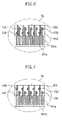
- FIGS. 4 through 9 are detailed enlarged views of a portion “Te” of FIG. 2 , which illustrate the stacked semiconductor module shown in FIG. 3 ;
- FIG. 10 is a cross-sectional view taken along line II-II′ of FIG. 4 ;
- FIG. 11 is a cross-sectional view taken along line III-III′ of FIG. 4 ;
- FIG. 12 is a cross-sectional view taken along line I-I′ of FIG. 2 , which illustrates a stacked semiconductor module according to another example embodiment
- FIGS. 13 through 16 are detailed enlarged views of a portion “Te” of FIG. 2 , which illustrate the stacked semiconductor module shown in FIG. 12 ;
- FIG. 17 is a cross-sectional view taken along line II-II′ of FIG. 4 , which illustrates the stacked semiconductor module shown in FIG. 12 ;
- FIG. 18 is a cross-sectional view taken along line III-III′ of FIG. 4 , which illustrates the stacked semiconductor module shown in FIG. 12 ;
- FIGS. 19 and 20 are cross-sectional views taken along line I-I′, which illustrate stacked semiconductor modules according to other example embodiments.
- FIGS. 21 through 24 are cross-sectional views illustrating a method of fabricating a stacked semiconductor module according to yet another example embodiment.
- first, second, etc. may be used herein to describe various elements, components, regions, layers, and/or sections, these elements, components, regions, layers, and/or sections should not be limited by these terms. These terms are only used to distinguish one element, component, region, layer, and/or section from another element, component, region, layer, and/or section. Thus, a first element, component, region, layer, or section discussed below could be termed a second element, component, region, layer, or section without departing from the teachings of example embodiments.
- spatially relative terms such as “beneath”, “below”, “lower”, “above”, “upper”, and the like, may be used herein for ease of description to describe one element or feature's relationship to another element(s) or feature(s) as illustrated in the figures. It will be understood that the spatially relative terms are intended to encompass different orientations of the device in use or operation in addition to the orientation depicted in the figures. For example, if the device in the figures is turned over, elements described as “below” or “beneath” other elements or features would then be oriented “above” the other elements or features. Thus, the exemplary term “below” can encompass both an orientation of above and below. The device may be otherwise oriented (rotated 90 degrees or at other orientations) and the spatially relative descriptors used herein interpreted accordingly.
- Embodiments described herein will refer to plan views and/or cross-sectional views by way of ideal schematic views. Accordingly, the views may be modified depending on manufacturing technologies and/or tolerances. Therefore, example embodiments are not limited to those shown in the views, but include modifications in configuration formed on the basis of manufacturing processes. Therefore, regions exemplified in figures have schematic properties and shapes of regions shown in figures exemplify specific shapes or regions of elements, and do not limit example embodiments.
- FIG. 1 is a partial perspective view of an electronic system including a stacked semiconductor module and an electronic board according to example embodiments.
- FIG. 2 is a plan view of one surface of a stacked semiconductor module according to example embodiments.
- the electronic system may include an electronic board 41 , a stacked semiconductor module 300 , and connectors 43 .
- the connectors 43 may be mounted on the electronic board 41 and may function to electrically connect the stacked semiconductor module 300 with the electronic board 41 .
- the electronic board 41 may be a mainboard for a personal computer.
- the stacked semiconductor module 300 may include a first semiconductor module 100 and a second semiconductor module 200 .
- the first semiconductor module 100 may include a rigid printed circuit board (PCB) 50 and a plurality of semiconductor devices 71 and 73 .
- the semiconductor devices 71 and 73 may be regularly mounted on one surface or both surfaces of the rigid PCB 50 .
- a register 56 , a phase-locked loop (PLL) 55 , and/or an additional logic chip 54 may also be mounted on the rigid PCB 50 .
- the register 56 , the PLL 55 , and the additional logic chip 54 may be selectively mounted or selectively omitted.
- the second semiconductor module 200 may include a flexible PCB 60 and other semiconductor devices (not shown). Although the register 56 , the PLL 55 , and the additional logic chip 54 may be selectively mounted also on the flexible PCB 60 , a description thereof will be omitted for brevity.
- the rigid PCB 50 and the flexible PCB 60 may include tabs T 11 , T 21 , T 31 , T 34 , T 41 , T 44 , T 45 , T 51 , T 54 , and T 62 at their end.
- the tabs T 11 , T 21 , T 31 , T 34 , T 41 , T 44 , T 45 , T 51 , T 54 , and T 62 may be formed of copper (Cu), tungsten (W), tungsten nitride (WN), titanium (Ti), titanium nitride (TiN), tantalum (Ta), tantalum nitride (TaN), gold (Au), and/or a combination thereof.
- the tabs T 11 , T 21 , T 31 , T 34 , T 41 , T 44 , T 45 , T 51 , T 54 , and T 62 may be formed by coating Au on a Cu surface.
- the semiconductor devices 71 and 73 , the other semiconductor devices, the register 56 , the PLL 55 , and the additional logic chip 54 may be electrically connected in series or parallel with the tabs T 11 , T 21 , T 31 , T 34 , T 41 , T 44 , T 45 , T 51 , T 54 , and T 62 .
- the flexible PCB 60 may bend or fold to contact the rigid PCB 50 .
- a portion of the flexible PCB 60 may wrap an end portion of the rigid PCB 50 .
- the tabs T 11 , T 21 , T 31 , T 34 , T 41 , T 44 , T 45 , T 51 , T 54 , and T 62 may be partially exposed at an end portion of the stacked semiconductor module 300 .
- the stacked semiconductor module 300 may be inserted into each of the connectors 43 .
- the semiconductor devices 71 and 73 and the other semiconductor devices may be electrically connected to the electronic board 41 by the tabs T 11 , T 21 , T 31 , T 34 , T 41 , T 44 , T 45 , T 51 , T 54 , and T 62 and the connectors 43 .
- the semiconductor devices 71 and 73 and the other semiconductor devices may be memory devices.
- the first semiconductor module 100 and/or the second semiconductor module 200 may be memory modules.
- the semiconductor devices 71 and 73 may be mounted in equal numbers.
- the semiconductor devices 71 and 73 may be mounted in equal number to 4, 8, 9, 16, 18, or a multiple thereof on the rigid PCB 50
- other semiconductor devices may be mounted in equal number to 4, 8, 9, 16, 18, or a multiple thereof on the flexible PCB 60 .
- the stacked semiconductor module 300 may be a stacked memory module.
- FIG. 3 is a cross-sectional view taken along line I-I′ of FIG. 2 , which illustrates a stacked semiconductor module according to an example embodiment.
- FIGS. 4 through 9 are detailed enlarged views of a portion “Te” of FIG. 2 , which illustrate the stacked semiconductor module shown in FIG. 3 .
- FIG. 10 is a cross-sectional view taken along line II-II′ of FIG. 4 .
- FIG. 11 is a cross-sectional view taken along line III-III′ of FIG. 4 .
- the stacked semiconductor module according to example embodiment 1 may include a first semiconductor module 100 , a second semiconductor module 200 A, and a third semiconductor module 200 B.
- the first semiconductor module 100 may include a rigid PCB 50 with first through fourth semiconductor devices 71 , 72 , 73 , and 74 .
- the rigid PCB 50 may include first via plugs P 31 and first and second tabs T 41 and T 31 .
- the semiconductor devices 71 , 72 , 73 , and 74 may be mounted on the rigid PCB 50 using conductive connection units, for example, solder balls 59 .
- the semiconductor devices 71 , 72 , 73 , and 74 may be electrically connected to the first and second tabs T 41 and T 31 by the solder balls 59 and embedded interconnection lines (not shown) of the rigid PCB 50 .
- the rigid PCB 50 may have a first surface 501 on one face of the rigid PCB 50 and a second surface 502 on an opposite face of the rigid PCB 50 .
- the first tabs T 41 may be formed on the first surface 501 and the second tabs T 31 may be formed on the second surface 502 .
- the first and second tabs T 41 and T 31 may be formed across from each other at an end portion of the rigid PCB 50 .
- the first via plugs P 31 may be in contact with the first and second tabs T 31 and T 41 through the rigid PCB 50 .
- the first via plugs P 31 may be formed adjacent to the tabs T 41 and T 31 and between the semiconductor devices 71 , 72 , 73 , and 74 and the tabs T 41 and T 31 .
- the first via plugs P 31 may be formed of Cu, W, WN, Ti, TiN, Ta, TaN, and/or a combination thereof.
- the semiconductor devices 71 , 72 , 73 , and 74 may be regularly mounted on one surface or both surfaces of the rigid PCB 50 .
- first and third semiconductor devices 71 and 73 may be mounted on the first surface 501 of the rigid PCB 50
- second and fourth semiconductor devices 72 and 74 may be mounted on the second surface 502 thereof.
- the second and third semiconductor modules 200 A and 200 B may include flexible PCBs 60 A and 60 B and fifth through twelfth semiconductor devices 81 , 82 , 83 , 84 , 85 , 86 , 87 , and 88 .
- the flexible PCB 60 A may have a third surface 601 on one face of the flexible PCB 60 A and a fourth surface 602 on an opposite face of the flexible PCB 60 A.
- the flexible PCB 60 B may include a fifth surface 603 on one face of the flexible PCB 60 B and a sixth surface 604 on opposite face of the flexible PCB 60 B.
- Each of the flexible PCBs 60 A and 60 B may include a subsidiary board 67 .
- the flexible PCBs 60 A and 60 B may include second via plugs P 11 and third through sixth tabs T 21 , T 11 , T 51 , and T 62 .
- the subsidiary board 67 may be formed using prepreg and/or Cu foil.
- the subsidiary board 67 may be partially bonded to each of the flexible PCBs 60 A and 60 B.
- the subsidiary board 67 may serve as a redistribution layer.
- the subsidiary board 67 may function to reduce the bending effect of the flexible PCBs 60 A and 60 B.
- portions of the flexible PCBs 60 A and 60 B to which the subsidiary boards 67 are bonded may be stiffened.
- the flexible PCBs 60 A and 60 B may be called rigid-flexible PCBs.
- Portions of the flexible PCBs 60 A and 60 B on which the subsidiary boards 67 are not mounted may be defined as connection sections 60 F.
- the connection sections 60 F may easily bend.
- the subsidiary board 67 may be omitted.
- the flexible PCBs 60 A and 60 B may bend or fold to contact the rigid PCB 50 .
- the flexible PCBs 60 A and 60 B may bend to wrap an end portion of the rigid PCB 50 .
- each of the flexible PCBs 60 A and 60 B may overlap the rigid PCB 50 .
- the flexible PCBs 60 A and 60 B may cover both surfaces of the rigid PCB 50 .
- the fifth tabs T 51 may face the first tabs T 41
- the third tabs T 21 may face the second tabs T 31 .
- the flexible PCBs 60 A and 60 B may be bonded to the rigid PCB 50 using a conductive adhesive 91 .
- the conductive adhesive 91 may include an anisotropic conductive film (ACF) or anisotropic conductive paste (ACP).
- ACF anisotropic conductive film
- ACP anisotropic conductive paste
- the conductive adhesive 91 may be bonded between the fifth tabs T 51 and the first tabs T 41 and between the third tabs T 21 and the second tabs T 31 .
- the conductive adhesive 91 may electrically connect the fifth tabs T 51 with the first tabs T 41 and electrically connect the third tabs T 21 with the second tabs T 31 .
- the third tabs T 21 may be formed on the third surface 601
- the fourth tabs T 11 may be formed on the fourth surface 602 .
- the third tabs T 21 and fourth tabs T 11 may be formed across from on another on the flexible PCB 60 A.
- the fifth tabs T 51 may be formed on the fifth surface 603
- the sixth tabs T 62 may be formed on the sixth surface 604 .
- the fifth and sixth tabs T 51 and T 62 may be formed across from one another on the flexible PCB 60 B.
- the second via plugs P 11 may be in contact with the third and fourth tabs T 21 and T 11 through the flexible PCB 60 A.
- the second via plugs P 11 may be formed adjacent to the tabs T 21 and T 11 .
- the second via plugs P 11 may also be formed between the semiconductor devices 81 , 82 , 83 , and 84 and the tabs T 21 and T 11 .
- the second via plugs P 11 may be formed of Cu, W, WN, Ti, TiN, Ta, TaN, and/or a combination thereof.
- the fifth through twelfth semiconductor devices 81 , 82 , 83 , 84 , 85 , 86 , 87 , and 88 may be regularly mounted on one surface or both surfaces of the flexible PCBs 60 A and 60 B.
- the sixth and eighth semiconductor devices 82 and 84 may be mounted on the third surface 601 of the flexible PCB 60 A to face the second and fourth semiconductor devices 72 and 74
- the fifth and seventh semiconductor devices 81 and 83 may be mounted on the fourth surface 602 of the flexible PCB 60 A across from the sixth and eighth semiconductor devices 82 and 84 .
- the tenth and twelfth semiconductor devices 86 and 88 may be mounted on the fifth surface 603 of the flexible PCB 60 B to face first and third semiconductor devices 71 and 73
- the ninth and eleventh semiconductor devices 85 and 87 may be mounted on the sixth surface 604 of the flexible PCB 60 B across from the tenth and twelfth semiconductor devices 86 and 88 .
- the fifth through twelfth semiconductor devices 81 , 82 , 83 , 84 , 85 , 86 , 87 , and 88 may be mounted on the flexible PCBs 60 A and 60 B using conductive connection units, such as the solder balls 59 .
- the fifth through twelfth semiconductor devices 81 , 82 , 83 , 84 , 85 , 86 , 87 , and 88 may be electrically connected to the third through sixth tabs T 21 , T 11 , T 51 , and T 62 by the solder balls 59 and embedded interconnection lines (not shown) of the flexible PCBs 60 A and 60 B.
- the second and third semiconductor modules 200 A and 200 B may be bonded to the first semiconductor module 100 using an adhesive plate 93 .
- the adhesive plate 93 may be formed between the second semiconductor device 72 and the sixth semiconductor device 82 and between the fourth semiconductor device 74 and the eighth semiconductor device 84 .
- the adhesive plate 93 may be formed between the first semiconductor device 71 and the tenth semiconductor device 86 and between the third semiconductor device 73 and the twelfth semiconductor device 88 .
- the adhesive plate 93 may be an adhesive tape functioning as a heat sink.
- a number N of fourth tabs T 11 may be formed on the fourth surface 602 .
- N may be an integer ranging from 2 to 1000.
- one hundred and twenty fourth tabs T 11 may be formed on the fourth surface 602 .
- the fourth tabs T 11 may be electrically connected to the fifth to eighth semiconductor devices 81 , 82 , 83 , and 84 by internal interconnection lines L 11 .
- the second via plugs P 11 may be in contact with the internal interconnection lines L 11 , respectively.
- the internal interconnection lines L 11 may be formed of Cu, W, WN, Ti, TiN, Ta, TaN, and/or a combination thereof.
- a number M of third tabs T 21 may be formed on the third surface 601 .
- the third tabs T 21 may include a first group of third tabs T 21 a and a second group of third tabs T 21 b .
- M may be an integer ranging from 2 to 1000, which may be larger than N.
- two hundred and forty third tabs T 21 may be formed on the third surface 601 .
- the first group third tabs T 21 a may be in contact with the second via plugs P 11 through the internal interconnection lines L 21 .
- the first group of the third tabs T 21 a may be electrically connected to the fourth tabs T 11 by the second via plugs P 11 .
- a second group of third tabs T 21 b may be electrically connected to the fifth through eighth semiconductor devices 81 , 82 , 83 , and 84 by other internal interconnection lines L 22 .
- the second group of the third tabs T 21 b may include a number N of third tabs.
- the second group of the third tabs T 21 b may include one hundred and twenty third tabs.
- the first group of third tabs T 21 a and the second group of third tabs T 21 b may be arranged alternately on the third surface 601 .
- the first group of the third tabs T 21 a may include third tabs in equal number to the fourth tabs T 11 .
- the first group of third tabs T 21 a may include a number N of third tabs.
- first group of third tabs T 21 a may include one hundred and twenty third tabs.
- a pitch between the first group of third tabs T 21 a and the second group of third tabs T 21 b may be smaller than a pitch between the fourth tabs T 11 .
- the width of the tabs in the first group of third tabs T 21 a and the width of the tabs in the second group of third tabs T 21 b may be smaller than that of the fourth tabs T 11 .
- a number K of second tabs T 31 may be formed on the second surface 502 .
- K may be an integer ranging from 2 to 1000, which may be larger than N.
- K may be equal to M.
- the second tabs T 31 may include a first group second tabs T 31 a and a second group of second tabs T 31 b .
- the first group of second tabs T 31 a may be electrically connected to the first through fourth semiconductor devices 71 , 72 , 73 , and 74 by internal interconnection lines L 31 .
- the first group of the second tabs T 31 a may be connected to the first via plugs P 31 by the internal interconnection lines L 31 .
- the second group of the second tabs T 31 b may be in contact with third via plugs P 32 through other internal interconnection lines L 32 .
- the second group of the second tabs T 31 b may include second tabs in equal number to the second group of third tabs T 21 b.
- the tabs of the first group of second tabs T 31 a and the tabs of the second group of second tabs T 31 b may be arranged alternately on the second surface 502 .
- the first group of the second tabs T 31 a may include second tabs in equal number to the fourth tabs T 11 .
- the first group of second tabs T 31 a may include a number N of second tabs. Therefore, first group T 31 a may include one hundred and twenty second tabs.
- a pitch between the tabs of the first group of second tabs T 31 a and the tabs of the second group of second tabs T 31 b may be equal to a pitch between the tabs of the first group of third tabs T 21 a and the second group of third tabs T 21 b .
- the width of the second tabs in groups T 31 a and T 31 b may be equal to that of the third tabs in groups T 21 a and T 21 b.
- a number L of first tabs T 41 may be formed on the first surface 501 .
- L may be an integer ranging from 2 to 1000, which may be larger than N.
- L may be equal to K.
- L may be equal to M.
- two hundred and forty first tabs T 41 may be formed on the first surface 501 .
- the first tabs T 41 may include a first group of first tabs T 41 a and a second group of first tabs T 41 b .
- a first group of the first tabs T 41 a may be connected to the first via plugs P 31 by internal interconnection lines L 41 .
- a second group of the first tabs T 41 b may be electrically connected to the first through fourth semiconductor devices 71 , 72 , 73 , and 74 by other internal interconnection lines L 42 .
- the second group of the first tabs T 41 b may be in contact with the third via plugs P 32 through the internal interconnection lines L 42 .
- the second group of the first tabs T 41 b may include first tabs in equal number to the second tabs of the second group of second tabs T 31 b .
- the second group of the first tabs T 41 b may be electrically connected to the second group of the second tabs T 31 b by the third via plugs P 32 .
- the first tabs of the first group T 41 a and the first tabs of the second group T 41 b may be arranged alternately on the first surface 501 .
- the first group of the first tabs T 41 a may include first tabs in equal number to the fourth tabs T 11 .
- the first group T 41 a may include a number N of first tabs. Therefore, the first group T 41 a may include one hundred and twenty first tabs.
- a pitch between the tabs of the first group of first tabs T 41 a and the tabs of the second group of first tabs T 41 b may be equal to a pitch between the second tabs in groups T 31 a and T 31 b .
- the width of the tabs of the first group of first tabs T 41 a and the width of the tabs of the second group of first tabs T 41 b may be equal to that of the second tabs in groups T 31 a and T 31 b.
- a number G of fifth tabs T 51 may be formed on the fifth surface 603 .
- G may be an integer ranging from 2 to 1000, which may be larger than N.
- G may be equal to L.
- G may be equal to K.
- G may be equal to M.
- the fifth tabs T 51 may include a first group of fifth tabs T 51 a and a second group of fifth tabs T 51 b .
- the first group of the fifth tabs T 51 a may be electrically connected to the ninth through twelfth semiconductor devices 85 , 86 , 87 , and 88 by internal interconnection lines L 51 .
- the second group of the fifth tabs T 51 b may be connected to fourth via plugs P 52 by other internal interconnection lines L 52 .
- the second group of the fifth tabs T 51 b may include fifth tabs in equal number to the first tabs of the second group of the first tabs T 41 b.
- the fifth tabs in groups T 51 a and T 51 b may be arranged alternately on the fifth surface 603 .
- the first group of the fifth tabs T 51 a may include fifth tabs in equal number to the fourth tabs T 11 .
- the first group T 51 a may include a number N of fifth tabs. Therefore, the first group T 51 a may include 120 fifth tabs.
- a pitch between the fifth tabs in groups T 51 a and T 51 b may be equal to a pitch between the first tabs in groups T 41 a and T 41 b .
- the width of the fifth tabs in groups T 51 a and T 51 b may be equal to that of the first tabs in groups T 41 a and T 41 b.
- a number H of sixth tabs T 62 may be formed on the sixth surface 604 .
- H may be an integer ranging from 2 to 1000.
- the sixth tabs T 62 may be electrically connected to the ninth to twelfth semiconductor devices 85 , 86 , 87 , and 88 by internal interconnection lines L 62 .
- the fourth via plugs P 52 may be in contact with the internal interconnection lines L 62 .
- the sixth tabs T 62 may be electrically connected to the second group of the fifth tabs T 51 b by the fourth via plugs P 52 .
- a pitch between the sixth tabs T 62 may be equal to a pitch between the fourth tabs T 11 .
- the first group of the first tabs T 41 a may be electrically connected to the first group of the second tabs T 31 a via the first via plugs P 31 formed through the rigid PCB 50 .
- the first group of the third tabs T 21 a may be electrically connected to the fourth tabs T 11 via the second via plugs P 11 formed through the flexible PCB 60 A.
- the first group of the third tabs T 21 a may be electrically connected to the first group of the second tabs T 31 a by the conductive adhesive 91 .
- the first group of the first tabs T 41 a may be electrically connected to the first group of the fifth tabs T 51 a by the conductive adhesive 91 .
- the fourth tabs T 11 may be electrically connected to the first through twelfth semiconductor devices 71 , 72 , 73 , 74 , 81 , 82 , 83 , 84 , 85 , 86 , 87 , and 88 via the first and second via plugs P 31 and P 11 , the conductive adhesive 91 , and the internal interconnection lines L 11 , L 21 , L 31 , L 41 , and L 51 .
- the surfaces of the rigid PCB 50 and the flexible PCBs 60 A and 60 B may be covered with an insulating layer 7 .
- the surfaces of the fourth tabs T 11 and the sixth tabs T 62 may be covered with a conductive layer with low corrosiveness and oxidation properties, for example, an Au layer 8 .
- the second group of the first tabs T 41 b may be electrically connected to the second group of the second tabs T 31 b via the third via plugs P 32 formed through the rigid PCB 50 .
- the second group of the fifth tabs T 51 b may be electrically connected to the sixth tabs T 62 via the fourth via plugs P 52 formed through the flexible PCB 60 B.
- the second group of the third tabs T 21 b may be electrically connected to the second group of the second tabs T 31 b by the conductive adhesive 91 .
- the second group of the first tabs T 41 b may be electrically connected to the second group of the fifth tabs T 51 b by the conductive adhesive 91 .
- the sixth tabs T 62 may be electrically connected to the first through twelfth semiconductor devices 71 , 72 , 73 , 74 , 81 , 82 , 83 , 84 , 85 , 86 , 87 , and 88 via the third and fourth via plugs P 32 and P 52 , the conductive adhesive 91 , and the internal interconnection lines L 22 , L 32 , L 42 , L 52 , and L 62 .
- the stacked semiconductor module according to Example embodiment 1 may be a double-data-rate two (DDR-2) memory module.
- the first through twelfth semiconductor devices 71 , 72 , 73 , 74 , 81 , 82 , 83 , 84 , 85 , 86 , 87 , and 88 may be memory devices, such as dynamic random access memory (DRAM) devices.
- the first through twelfth semiconductor devices 71 , 72 , 73 , 74 , 81 , 82 , 83 , 84 , 85 , 86 , 87 , and 88 may be single memory chips or multi-chip packages (MCPs).
- Each of the flexible PCBs 60 A and 60 B may be thinner than the rigid PCB 50 .
- the rigid PCB 50 may have a thickness of about 0.6 mm
- each of the flexible PCBs 60 A and 60 B may have a thickness of about 0.3 mm.
- One hundred and twenty fourth tabs T 11 and one hundred and twenty sixth tabs T 62 may be provided, and two hundred and forty first tabs T 41 , two hundred and forty second tabs T 31 , two hundred and forty third tabs T 21 , and two hundred and forty fifth tabs T 51 may be provided.
- each of the first group of the first tabs T 41 a , the second group of the first tabs T 41 b , the first group of the second tabs T 31 a , the second group of the second tabs T 31 b , the first group of the third tabs T 21 a , the second group of the third tabs T 21 b , the first group of the fifth tabs T 51 a , and the second group of the fifth tabs T 51 b may include two hundred and twenty tabs.
- the fourth tabs T 11 , the first group of the third tabs T 21 a , the first group of the second tabs T 31 a , the first group of the first tabs T 41 a , and the first group of the fifth tabs T 51 a may be electrically connected to one another by the first and second via plugs P 31 and P 11 and the conductive adhesive 91 .
- the sixth tabs T 62 , the second group of the fifth tabs T 51 b , the second group of the first tabs T 41 b , the second group of the second tabs T 31 b , and the second group of the third tabs T 21 b may be electrically connected to one another by the third and fourth via plugs P 32 and P 52 and the conductive adhesive 91 .
- the fourth tabs T 11 may be electrically connected to the first through twelfth semiconductor devices 71 , 72 , 73 , 74 , 81 , 82 , 83 , 84 , 85 , 86 , 87 , and 88 via the first and second via plugs P 31 and P 11 ), the conductive adhesive 91 , and the internal interconnection lines L 11 , L 21 , L 31 , L 41 , and L 51 .
- the sixth tabs T 62 may be electrically connected to the first through twelfth semiconductor devices 71 , 72 , 73 , 74 , 81 , 82 , 83 , 84 , 85 , 86 , 87 , and 88 via the third and fourth via plugs P 32 and P 52 , the conductive adhesive 91 , and the internal interconnection lines L 22 , L 32 , L 42 , L 52 , and L 62 .
- the first through fourth via plugs P 31 , P 11 , P 32 , and P 52 may be formed adjacent to the first through sixth tabs T 11 , T 21 , T 31 , T 41 , T 51 , and T 62 .
- the first through fourth via plugs P 31 , P 11 , P 32 , and P 52 may greatly shorten electrical connection paths between the first through twelfth semiconductor devices 71 , 72 , 73 , 74 , 81 , 82 , 83 , 84 , 85 , 86 , 87 , and 88 and the fourth tabs T 11 and electrical connection paths between the first through twelfth semiconductor devices 71 , 72 , 73 , 74 , 81 , 82 , 83 , 84 , 85 , 86 , 87 , and 88 and the sixth tabs T 62 .
- a high-capacity stacked memory module can be embodied.
- FIG. 12 is a cross-sectional view taken along line I-I′ of FIG. 2 , which illustrates a stacked semiconductor module according to another example embodiment.
- FIGS. 13 through 16 are detailed enlarged views of a portion “Te” of FIG. 2 , which illustrate the stacked semiconductor module shown in FIG. 12 .
- FIG. 17 is a cross-sectional view taken along line II-II′ of FIG. 4 , which illustrates the stacked semiconductor module shown in FIG. 12 .
- FIG. 18 is a cross-sectional view taken along line III-III′ of FIG. 4 , which illustrates the stacked semiconductor module shown in FIG. 12 .
- the stacked semiconductor module according to example embodiment 2 may include a first semiconductor module 100 and a second semiconductor module 200 .
- the same description as in Example embodiment 1 will be omitted.
- the first semiconductor module 100 may include a rigid PCB 50 and first through fourth semiconductor devices 71 , 72 , 73 , and 74 .
- the rigid PCB 50 may include third via plugs P 32 and first and second tabs T 44 , T 45 , and T 34 .
- the semiconductor devices 71 , 72 , 73 , and 74 may be electrically connected to the tabs T 44 , T 45 , and T 34 by solder balls 59 and embedded interconnection lines (not shown) of the rigid PCB 50 .
- the rigid PCB 50 may have a first surface 501 on one face of the rigid PCB 50 and a second surface 502 on an opposite face of the rigid PCB 50 .
- the third via plugs P 32 may be in contact with the first and second tabs T 44 , T 45 , and T 34 through the rigid PCB 50 .
- the third via plugs P 32 may be formed adjacent to the tabs T 44 , T 45 , and T 34 between the semiconductor devices 71 , 72 , 73 , and 74 and the tabs T 44 , T 45 , and T 34 .
- the third via plugs P 32 may be formed of Cu, W, WN, Ti, TiN, Ta, TaN, and/or a combination thereof.
- the second semiconductor module 200 may include a flexible PCB 60 and fifth through eighth semiconductor devices 81 , 82 , 83 , and 84 .
- the flexible PCB 60 may include a third surface 601 and a fourth surface 602 , which are on opposite faces of the flexible PCB 60 , and a fifth surface 603 and a sixth surface 604 , which are on opposite faces of the flexible PCB 60 .
- the flexible PCB 60 may include a subsidiary board 67 .
- the flexible PCB 60 may include fourth via plugs P 52 and third through sixth tabs T 21 , T 11 , T 54 , and T 62 .
- the subsidiary board 67 may be formed using prepreg and Cu foil. However, according to other example embodiments, the subsidiary board 67 may be omitted.
- the flexible PCB 60 may bend or fold to contact the rigid PCB 50 .
- the flexible PCB 60 may fold to wrap an end portion of the rigid PCB 50 .
- the flexible PCB 60 may overlap the rigid PCB 50 .
- the flexible PCB 60 may be bonded to the rigid PCB 50 using a conductive adhesive 91 .
- the conductive adhesive 91 may include an ACF or ACP.
- the conductive adhesive 91 may be bonded between the fifth tabs T 54 and the first tabs T 44 and T 45 and between the third tabs T 21 and the second tabs T 34 .
- the conductive adhesive 91 may electrically connect the fifth tabs T 54 with the first tabs T 44 and T 45 and electrically connect the third tabs T 21 with the second tabs T 34 .
- the fourth via plugs P 52 may be in contact with the fifth and sixth tabs T 54 and T 62 through the flexible PCB 60 .
- the fourth via plugs P 52 may be formed adjacent to the fifth and sixth tabs T 54 and T 62 .
- the fourth via plugs P 52 may be formed of Cu, W, WN, Ti, TiN, Ta, TaN, and/or a combination thereof.
- the fifth through eighth semiconductor devices 81 , 82 , 83 , and 84 may be mounted on the flexible PCB 60 using conductive connection units, such as the solder balls 59 .
- the second semiconductor module 200 may be bonded to the first semiconductor module 100 using an adhesive plate 93 .
- the adhesive plate 93 may be an adhesive tape functioning as a heat sink.
- a number N of fourth tabs T 11 , internal interconnection lines L 11 , and second via plugs P 11 may be formed on the fourth surface 602 .
- N may be an integer ranging from 2 to 1000.
- a number M of third tabs T 21 , internal interconnection lines L 21 and L 22 , and second via plugs P 11 which are the same as described with reference to FIG. 5 , may be formed on the third surface 601 , wherein the groups T 21 a and T 21 b are different groups of third tabs T 21 .
- M may be an integer ranging from 2 to 1000, which may be larger than N.
- a number K of second tabs T 34 may be formed on the second surface 502 .
- the second tabs T 34 may include a first group of second tabs T 34 b and a second group of second tabs 34 a .
- K may be an integer ranging from 2 to 1000, which may be larger than N.
- K may be equal to M.
- the first group of the second tabs T 34 b may be electrically connected to the first through fourth semiconductor devices 71 , 72 , 73 , and 74 by internal interconnection lines L 33 .
- a second group of the second tabs T 34 a may be in contact with the third via plugs P 32 through other internal interconnection lines L 34 .
- the second group of the second tabs T 34 a may include second tabs in equal number to the third tabs of the second group of the third tabs T 21 b.
- the first group of second tabs T 34 b and the second group of second tabs T 34 a may be arranged alternately one by one on the second surface 502 .
- the first group of the second tabs T 34 b may include second tabs in equal number to the fourth tabs T 11 .
- the first group T 34 b may include a number N of second tabs. Therefore, the first group T 34 b may include one hundred and twenty second tabs.
- a pitch between the second tabs T 34 may be equal to a pitch between the third tabs T 21 .
- the width of the second tabs in groups T 34 a and T 34 b may be equal to the width of the tabs in groups T 21 a and T 21 b.
- first tabs T 44 may be formed on the first surface 501 .
- the first tabs T 44 may include a first group of first tabs T 44 b and a second group of first tabs T 44 a .
- L may be an integer ranging from 2 to 1000, which may be larger than N.
- L may be equal to K.
- L may be equal to M.
- two hundred and forty first tabs T 44 may be formed on the first surface 501 .
- a second group of the first tabs T 44 a may be electrically connected to the first through fourth semiconductor devices 71 , 72 , 73 , and 74 by internal interconnection lines L 44 .
- the second group of the first tabs T 44 a may be in contact with the third via plugs P 32 through the internal interconnection lines L 44 .
- the second group of the first tabs T 44 a may include first tabs in equal number to the second tabs of the second group of the second tabs T 34 a .
- the second group of the first tabs T 44 a may be electrically connected to the second group of the second tabs T 34 a by the third via plugs P 32 .
- the first tabs of a first group T 44 b and the first tabs of the second group T 44 a may be arranged alternately one by one on the first surface 501 .
- the first group of the first tabs T 44 b may include first tabs in equal number to the second tabs of the first group of the second tabs T 34 b .
- a pitch between the first tabs T 44 may be equal to a pitch between the second tabs T 34 .
- the width of the first tabs T 44 may be equal to that of the second tabs T 34 .
- a number G′ of fifth tabs T 54 may be formed on the fifth surface 603 .
- G′ may be an integer ranging from 2 to 1000.
- G′ may be equal to N.
- the fifth tabs T 54 may be connected to the fourth via plugs P 52 by internal interconnection lines L 54 .
- the fifth tabs T 54 may be provided in equal number to the first tabs of the second group of the first tabs T 44 a .
- a pitch between the fifth tabs T 54 may be greater than a pitch between the first tabs T 44 .
- the width of the fifth tabs T 54 may be equal to that of the fourth tabs T 11 .
- H may be an integer ranging from 2 to 1000.
- one hundred and twenty sixth tabs T 62 may be formed on the sixth surface 604 .
- the sixth tabs T 62 may be electrically connected to the fifth tabs T 54 by the fourth via plugs P 52 .
- a pitch between the sixth tabs T 62 may be equal to a pitch between the fifth tabs T 54 and a pitch between the fourth tabs T 11 .
- a number L′ of first tabs T 45 may be formed on the first surface 501 .
- L′ may be an integer ranging from 2 to 1000.
- L′ may be equal to G′ and H.
- one hundred and twenty first tabs T 45 may be formed on the first surface 501 .
- the first tabs T 45 may be electrically connected to the first through fourth semiconductor devices 71 , 72 , 73 , and 74 by internal interconnection lines L 45 .
- the first tabs T 45 may be in contact with the third via plugs P 32 through the internal interconnection lines L 45 .
- the first tabs T 45 may be provided in equal number to the second tabs of the second group of the second tabs T 34 a .
- the first tabs T 45 may be electrically connected to the second group of the second tabs T 34 a by the third via plugs P 32 .
- a pitch between the first tabs T 45 may be greater than a pitch between the second tabs T 34 .
- the width of the first tabs T 45 may be equal to that of the fourth tabs T 11 .
- a first group of the third tabs T 21 a may be electrically connected to the fourth tabs T 11 via the second via plugs P 11 formed through the flexible PCB 60 .
- the first group of the third tabs T 21 a may be electrically connected to the first group of the second tabs T 34 b by the conductive adhesive 91 .
- the first tabs T 44 b , T 44 a , and T 45 may be electrically connected to the fifth tabs T 54 by the conductive adhesive 91 .
- the fourth tabs T 11 may be electrically connected to the first through eighth semiconductor devices 71 , 72 , 73 , 74 , 81 , 82 , 83 , and 84 via the second via plugs P 11 , the conductive adhesive 91 , and the internal interconnection lines L 11 , L 21 , and L 33 .
- the surfaces of the rigid PCB 50 and the flexible PCB 60 may be covered with an insulating layer 7 .
- the surfaces of the fourth tabs T 11 and the sixth tabs T 62 may be covered with a conductive layer with low corrosiveness and oxidation properties, for example, an Au layer 8 .
- the second group of the first tabs T 44 a and T 45 may be electrically connected to the second group of the second tabs T 34 a via the third via plugs P 32 formed through the rigid PCB 50 .
- the fifth tabs T 54 may be electrically connected to the sixth tabs T 62 via the fourth via plugs P 52 formed through the flexible PCB 60 .
- the second group of the third tabs T 21 b may be electrically connected to the second group of the second tabs T 34 a by the conductive adhesive 91 .
- the first tabs T 44 a , T 44 b , and T 45 may be electrically connected to the fifth tabs T 54 by the conductive adhesive 91 .
- the sixth tabs T 62 may be electrically connected to the first through eighth semiconductor devices 71 , 72 , 73 , 74 , 81 , 82 , 83 , and 84 via the third and fourth via plugs P 32 and P 52 and the internal interconnection lines L 22 , L 34 , L 44 , L 45 , L 54 , and L 62 .
- the stacked semiconductor module according to Example embodiment 2 may be a DDR-2 memory module.
- the first through eighth semiconductor devices 71 , 72 , 73 , 74 , 81 , 82 , 83 , and 84 may be DRAM devices.
- the first through eighth semiconductor devices 71 , 72 , 73 , 74 , 81 , 82 , 83 , and 84 may be single memory chips or MCPs.
- the flexible PCB 60 may be thinner than the rigid PCB 50 .
- One hundred and twenty fourth tabs T 11 , one hundred and twenty fifth tabs T 54 , and one hundred and twenty sixth tabs T 62 may be provided, and two hundred and forty first tabs T 44 , two hundred and forty second tabs T 34 , and two hundred and forty third tabs T 21 may be provided.
- each of the first group of the first tabs T 44 b , the second group of the first tabs T 44 a , the first group of the second tabs T 34 b , the second group of the second tabs T 34 a , the first group of the third tabs T 21 a , and the second group of the third tabs T 21 b may include one hundred and twenty tabs.
- one hundred and twenty first tabs T 45 may be provided.
- the fourth tabs T 11 , the first group of the third tabs T 21 a , and the first group of the second tabs T 34 b may be electrically connected to one another by the second via plugs P 11 and the conductive adhesive 91 .
- the sixth tabs T 62 , the fifth tabs T 54 , the first tabs T 44 b , T 44 a , and T 45 , the second group of the second tabs T 34 a , and the second group of the third tabs T 21 b may be electrically connected to one another by the third and fourth via plugs P 32 and P 52 and the conductive adhesive 91 .
- the fourth tabs T 11 may be electrically connected to the first through eighth semiconductor devices 71 , 72 , 73 , 74 , 81 , 82 , 83 , and 84 via the second via plugs P 11 , the conductive adhesive 91 , and the internal interconnection lines L 11 , L 21 , and L 33 .
- the sixth tabs T 62 may be electrically connected to the first through eighth semiconductor devices 71 , 72 , 73 , 74 , 81 , 82 , 83 , and 84 via the third and fourth via plugs P 32 and P 52 , the conductive adhesive 91 , and the internal interconnection lines L 22 , L 34 , L 44 , L 45 , L 54 , and L 62 .
- the second through fourth via plugs P 11 , P 32 , and P 52 may be formed adjacent to the first through sixth tabs T 11 , T 21 , T 34 , T 44 (T 45 ), T 54 , and T 62 .
- the second through fourth via plugs P 11 , P 32 , and P 52 may greatly shorten electrical connection paths between the first through eighth semiconductor devices 71 , 72 , 73 , 74 , 81 , 82 , 83 , and 84 and the fourth tabs T 11 and electrical connection paths between the first through eighth semiconductor devices 71 , 72 , 73 , 74 , 81 , 82 , 83 , and 84 and the sixth tabs T 62 .
- a high-capacity stacked memory module can be embodied.
- FIG. 19 is a cross-sectional view taken along line I-I′, which illustrates a stacked semiconductor module according to another example embodiment.
- the stacked semiconductor module according to Example embodiment 3 may include a first semiconductor module 100 , a second semiconductor module 200 C, and a third semiconductor module 200 D.
- the first semiconductor module 100 may include a rigid PCB 50 , first through fourth semiconductor devices 71 , 72 , 73 , and 74 , third via plugs P 32 , and first and second tabs T 44 , T 45 , and T 34 , which are about the same as described in Example embodiment 2.
- the second semiconductor module 200 C may include a flexible PCB 60 D, fifth through eighth semiconductor devices 81 , 82 , 83 , and 84 , a subsidiary board 67 , second via plugs (not shown), fourth via plugs P 52 , and third through sixth tabs T 21 , T 11 , T 54 , and T 62 , which are about the same as described in Example embodiment 2.
- One end portion of the flexible PCB 60 D may fold to wrap an end portion of the rigid PCB 50 .
- the flexible PCB 60 D may overlap the rigid PCB 50 .
- the flexible PCB 60 D may be bonded to the rigid PCB 50 using a conductive adhesive 91 .
- the second semiconductor module 200 C may be bonded to the first semiconductor module 100 using an adhesive plate 93 .
- the adhesive plate 93 may be bonded between the second semiconductor device 72 and the sixth semiconductor device 82 and between the fourth semiconductor device 74 and the eighth semiconductor device 84 .
- the third semiconductor module 200 D may include a flexible PCB 60 C, ninth through twelfth semiconductor devices 85 ′, 86 ′, 87 ′, and 88 ′, and a subsidiary board 67 .
- the flexible PCBs 60 C and 60 D may be connected to each other.
- the subsidiary board 67 may not be bonded to a connection section 60 F between the flexible PCBs 60 C and 60 D.
- the connection section 60 F may easily bend.
- the third semiconductor module 200 D may be bonded to the second semiconductor module 200 C using the adhesive plate 93 .
- the adhesive plate 93 may be bonded between the fifth semiconductor device 81 and the eleventh semiconductor device 87 ′ and between the seventh semiconductor device 83 and the ninth semiconductor device 85 ′.
- the flexible printed circuit board 60 C may include a first surface 603 ′ and a second surface 604 ′ on opposite faces of the flexible printed circuit board 60 C.
- the first surface 603 ′ may support the ninth and eleventh semiconductor devices 85 ′ and 87 ′ and the second surface may support the twelfth and tenth semiconductor devices 88 ′ and 86 ′.
- the flexible printed circuit board 60 D may include a first surface 602 and a second surface 601 on opposite faces of the flexible printed circuit board 60 D.
- the first surface 602 may support the fifth and seventh semiconductor devices 81 and 83 and the second surface 601 may support the sixth and eighth semiconductor devices 82 and 84 .
- FIG. 20 is a cross-sectional view taken along line I-I′, which illustrates a stacked semiconductor modules according to another example embodiment.
- the stacked semiconductor module according to example embodiment 4 may include a first semiconductor module 100 and a second semiconductor module 200 E.
- the first semiconductor module 100 may include a rigid PCB 50 , first through fourth semiconductor devices 71 , 72 , 73 , and 74 , third via plugs P 32 , and first and second tabs T 45 and T 34 , which are about the same as described in Example embodiment 2.
- the second semiconductor module 200 E may include a flexible PCB 60 E, fifth through eighth semiconductor devices 81 , 82 , 83 , and 84 , a subsidiary board 67 , second via plugs (not shown), and third and fourth tabs T 21 and T 11 , which are about the same as described in Example embodiment 2.
- One end portion of the flexible PCB 60 E may overlap an end portion of the rigid PCB 50 .
- the flexible PCB 60 E may be bonded to the rigid PCB 50 using a conductive adhesive 91 .
- the second semiconductor module 200 E may be bonded to the first semiconductor module 100 using an adhesive plate 93 .
- the adhesive plate 93 may be bonded between the second semiconductor device 72 and the sixth semiconductor device 82 and between the fourth semiconductor device 74 and the eighth semiconductor device 84 .
- a number L′ of first tabs T 45 may be formed on the first surface 501 in about the same manner as described with reference to FIG. 16 .
- L′ may be an integer ranging from 2 to 1000.
- one hundred and twenty first tabs T 45 may be formed on the first surface 501 .
- the first tabs T 45 may be electrically connected to the first through fourth semiconductor devices through internal interconnection lines L 45 .
- the first tabs T 45 may be in contact with the third via plugs P 32 through the internal interconnection lines L 45 .
- N may be an integer ranging from 2 to 1000.
- a number M of third tabs T 21 , internal interconnection lines L 21 and L 22 , and second via plugs P 1 , which are the same as described with reference to FIG. 5 may be formed on the third surface 601 .
- M may be an integer ranging from 2 to 1000, which may be larger than N.
- a number K of second tabs T 34 may be formed on the second surface 502 .
- K may be an integer ranging from 2 to 1000, which may be larger than L′.
- K may be equal to M.
- two hundred and forty second tabs T 34 may be formed on the second surface 502 .
- a first group of the second tabs T 34 b may be electrically connected to the first through fourth semiconductor devices 71 , 72 , 73 , and 74 by internal interconnection lines L 33 .
- a second group of the second tabs T 34 a may be in contact with the third via plugs P 32 through other internal interconnection lines L 34 .
- the second group of the second tabs T 34 a may include second tabs in equal number to the third tabs of the second group of the third tabs T 21 b . Also, the second group of the second tabs T 34 a may include second tabs in equal number to the first tabs T 45 .
- the second tabs of the first group T 34 b and the second tabs of the second group T 34 a may be arranged alternately on the second surface 502 .
- the first group of the second tabs T 34 b may include second tabs in equal number to the fourth tabs T 11 .
- the first group T 34 b may include a number N of second tabs. Therefore, the first group T 34 b may include one hundred and twenty second tabs.
- a pitch between the second tabs T 34 a and T 34 b may be equal to a pitch between the third tabs in groups T 21 a and T 21 b .
- the width of the second tabs in groups T 34 a and T 34 b may be equal to that of the third tabs in groups T 21 a and T 21 b.
- the stacked semiconductor module according to Example embodiment 4 may be a DDR-2 memory module.
- the first through eighth semiconductor devices 71 , 72 , 73 , 74 , 81 , 82 , 83 , and 84 may be DRAM devices.
- the first through eighth semiconductor devices 71 , 72 , 73 , 74 , 81 , 82 , 83 , and 84 may be single memory chips or MCPs.
- the flexible PCB 60 E may be thinner than the rigid PCB 50 .
- One hundred and twenty fourth tabs T 11 and one hundred and twenty first tabs T 45 may be provided, and two hundred and forty second tabs T 34 and two hundred and forty third tabs T 21 may be provided. Also, each of the first group of the second tabs T 34 b , the second group of the second tabs T 34 a , the first group of the third tabs T 21 a , and the second group of the third tabs T 21 b may include one hundred and twenty tabs.
- the fourth tabs T 11 , the first group of the third tabs T 21 a , and the first group of the second tabs T 34 b may be electrically connected to one another by the second via plugs P 11 and the conductive adhesive 91 .
- the first tabs T 45 , the second group of the second tabs T 34 a , and the second group of the third tabs T 21 b may be electrically connected to one another by the third via plugs P 32 and the conductive adhesive 91 .
- the fourth tabs T 11 may be electrically connected to the first through eighth semiconductor devices 71 , 72 , 73 , 74 , 81 , 82 , 83 , and 84 via the second via plugs P 11 , the conductive adhesive 91 , and the internal interconnection lines L 1 , L 21 , and L 33 .
- the first tabs T 45 may be electrically connected to the first through eighth semiconductor devices 71 , 72 , 73 , 74 , 81 , 82 , 83 , and 84 via the third via plugs P 32 , the conductive adhesive 91 , and the internal interconnection lines L 22 , L 34 , and L 45 .
- the second and third via plugs P 11 and P 32 may be formed adjacent to the first through fourth tabs T 11 , T 21 , T 34 , and T 45 .
- the second and third via plugs P 11 and P 32 may greatly shorten electrical connection paths between the first through eighth semiconductor devices 71 , 72 , 73 , 74 , 81 , 82 , 83 , and 84 and the fourth tabs T 11 and electrical connection paths between the first through eighth semiconductor devices 71 , 72 , 73 , 74 , 81 , 82 , 83 , and 84 and the first tabs T 45 .
- FIGS. 21 through 24 are cross-sectional views illustrating a method of fabricating a stacked semiconductor module according to yet another example embodiment.
- the stacked semiconductor module formed according to Example embodiment 5 may be almost the same as the stacked semiconductor module shown in FIG. 12 , according to example embodiment 2.
- a rigid PCB 50 and a flexible PCB 60 may be prepared.
- a subsidiary board 67 may be formed on a partial region of the flexible PCB 60 .
- a combination of the flexible PCB 60 and the subsidiary board 67 may be called a rigid-flexible PCB.
- the rigid PCB 50 may be formed to have third via plugs P 32 and first and second tabs T 45 and T 34 .
- the rigid PCB 50 may have a first surface 501 and a second surface 502 on opposite sides of the rigid printed circuit board 50 . The surfaces may be separated by the thickness t 1 of the rigid printed circuit board 50 .
- the first tabs T 45 may be the same as described with reference to FIG. 16
- the second tabs T 34 may be the same as described with reference to FIG. 13 .
- the third via plugs P 32 may be formed adjacent to the first and second tabs T 45 and T 34 to penetrate the rigid PCB 50 .
- the first tabs T 45 may be electrically connected to a second group of the second tabs T 34 a via the third via plugs P 32 .
- the third via plugs P 32 may be formed of Cu, W, WN, Ti, TiN, Ta, TaN, or a combination thereof.
- the rigid PCB 50 may be formed of a single or multiple prepreg layer and Cu foil formed therebetween.
- the first and second tabs T 45 and T 34 may be formed at an end portion of the rigid PCB 50 .
- the rigid PCB 50 may be formed to a thickness of about 0.6 mm.
- the flexible PCB 60 may be formed to have second via plugs (refer to P 11 in FIG. 17 ), fourth via plugs P 52 , and third through sixth tabs T 21 , T 11 , T 54 , and T 62 .
- the flexible PCB 60 may have a third surface 601 and a fourth surface 602 on opposite faces of the flexible PCB 60 and may be separated by the thickness t 2 of the flexible PCB 60 .
- the surfaces 601 and 602 may be separated by a thickness t 2 of the flexible PCB 60 .
- the third tabs T 21 may be the same as described with reference to FIG. 5
- the fourth tabs T 11 may be the same as described with reference to FIG. 4
- the fifth tabs T 54 may be the same as described with reference to FIG. 15
- the sixth tabs T 62 may be the same as described with reference to FIG. 18 .
- the flexible PCB 60 may be formed of a single or multiple flexible film and Cu foil interposed therebetween.
- the flexible PCB 60 may be formed to a thickness of about 0.3 mm, which is smaller than the thickness of the rigid PCB 50 .
- the second via plugs P 11 and the fourth via plugs P 52 may be formed through the flexible PCB 60 .
- the second via plugs P 11 may be formed adjacent to the third and fourth tabs T 21 and T 11 .
- the fourth via plugs P 52 may be formed adjacent to the fifth and sixth tabs T 54 and T 62 .
- the second via plugs P 11 and the fourth via plugs P 52 may be formed of Cu, W, WN, Ti, TiN, Ta, TaN, or a combination thereof.
- the fourth tabs T 11 may be electrically connected to a first group of the third tabs T 21 a via the second via plugs P 11 .
- the sixth tabs T 62 may be electrically connected to the fifth tabs T 54 via the fourth via plugs P 52 .
- the subsidiary board 67 may be formed by sequentially stacking prepreg and Cu foil.
- the subsidiary board 67 may serve as a redistribution layer.
- the subsidiary board 67 may function to reduce the bending effect of the flexible PCB 60 .
- a portion of the flexible PCB 60 to which the subsidiary board 67 is bonded may be relatively stiff.
- a process of forming the subsidiary board 67 may be omitted.
- the subsidiary board 67 may not be bonded to the third and sixth tabs T 21 , T 11 , T 54 , and T 62 and their adjacent regions.
- a portion of the flexible PCB 60 on which the subsidiary board 67 is not mounted may be defined as a connection section 60 F.
- the connection section 60 F may easily bend.
- the subsidiary board 67 may be formed on the surface of the flexible PCB 60 .
- the subsidiary board 67 may be embedded between a plurality of flexible films constituting the flexible PCB 60 , although a description thereof will be omitted for brevity.
- first through eighth semiconductor devices 71 , 72 , 73 , 74 , 81 , 82 , 83 , and 84 may be mounted on the rigid PCB 50 and the flexible PCB 60 using conductive connection units, for example, solder balls 59 .
- the fifth through eighth memory devices 81 , 82 , 83 , and 84 may be mounted on the subsidiary board 67 .
- a conductive adhesive 91 may be coated on the first through third tabs T 45 , T 34 , T 21 , and the fifth tabs T 54 .
- the conductive adhesive 91 may be formed of an ACF or ACP.
- the conductive adhesive 91 may be selectively omitted.
- An adhesive plate 93 may be bonded to the surfaces of the second semiconductor device 72 , the fourth semiconductor device 74 , the sixth semiconductor device 82 , and the eighth semiconductor device 84 .
- the adhesive plate 93 may be an adhesive tape functioning as a heat sink. In another case, the adhesive plate 93 may be selectively bonded to one or more of the surfaces of the second semiconductor device 72 , the fourth semiconductor device 74 , the sixth semiconductor device 82 , and the eighth semiconductor device 84 .
- the flexible PCB 60 may bend or fold to contact the rigid PCB 50 .
- an end portion of the flexible PCB 60 may fold to wrap an end portion of the rigid PCB 50 .
- the second tabs T 34 may face the third tabs T 21
- the first tabs T 45 may face the fifth tabs T 54 .
- the second tabs T 34 and the third tabs T 21 may be bonded to each other using the conductive adhesive 91
- the first tabs T 45 and the fifth tabs T 54 also may be bonded to each other using the conductive adhesive 91 .
- the conductive adhesive 91 may bond tabs using pressure and/or heat.
- the conductive adhesive 91 may function to provide mechanical/electrical connection between the first tabs T 45 and the fifth tabs T 54 and between the second tabs T 34 and the third tabs T 21 .
- the adhesive plate 93 may be connected between the second semiconductor device 72 and the sixth semiconductor device 82 and between the fourth semiconductor device 74 and the eighth semiconductor device 84 .
- the adhesive plate 93 may fix the semiconductor devices 72 , 82 , 74 , and 84 to one another.
- a stacked semiconductor module including first and second semiconductor modules is provided.
- the first semiconductor module includes a rigid PCB and a plurality of semiconductor devices mounted on the rigid PCB.
- the second semiconductor module includes a flexible PCB and a plurality of other semiconductor devices mounted on the flexible PCB.
- the flexible PCB is connected to the rigid PCB.
- the bending and folding properties of the flexible PCB facilitates the connection of the flexible PCB to the rigid PCB and ensures reliability.
- tabs of the rigid PCB are electrically connected to tabs of the flexible PCB by via plugs. As a result, signal transmission paths between the tabs and the semiconductor devices can be markedly shortened.
Landscapes
- Engineering & Computer Science (AREA)
- Microelectronics & Electronic Packaging (AREA)
- Wire Bonding (AREA)
Abstract
Description
Claims (18)
Applications Claiming Priority (4)
| Application Number | Priority Date | Filing Date | Title |
|---|---|---|---|
| KR10-2007-0098026 | 2007-09-28 | ||
| KR1020070098026A KR20090032638A (en) | 2007-09-28 | 2007-09-28 | Stacked memory module and method of forming the same |
| KR10-2008-0090880 | 2008-09-17 | ||
| KR20080090880A KR101483272B1 (en) | 2008-09-17 | 2008-09-17 | Stacked semiconductor module, method of forming the same, and an electronic system using the same |
Publications (2)
| Publication Number | Publication Date |
|---|---|
| US20090129041A1 US20090129041A1 (en) | 2009-05-21 |
| US7715200B2 true US7715200B2 (en) | 2010-05-11 |
Family
ID=40641730
Family Applications (1)
| Application Number | Title | Priority Date | Filing Date |
|---|---|---|---|
| US12/232,990 Active 2028-10-29 US7715200B2 (en) | 2007-09-28 | 2008-09-26 | Stacked semiconductor module, method of fabricating the same, and electronic system using the same |
Country Status (1)
| Country | Link |
|---|---|
| US (1) | US7715200B2 (en) |
Cited By (5)
| Publication number | Priority date | Publication date | Assignee | Title |
|---|---|---|---|---|
| US20120318562A1 (en) * | 2011-06-20 | 2012-12-20 | Samsung Electronics Co., Ltd. | Working panel and working panel set comprising array board patterns |
| US8730657B2 (en) | 2011-06-24 | 2014-05-20 | Blackberry Limited | Mobile computing devices |
| US9155194B1 (en) * | 2012-06-28 | 2015-10-06 | Emc Corporation | Memory interconnect arrangement having high data transfer speed signal integrity |
| US9496633B1 (en) * | 2015-06-22 | 2016-11-15 | Intel Corporation | Memory module adaptor card |
| US9504160B2 (en) | 2013-11-20 | 2016-11-22 | Samsung Electronics Co., Ltd. | Semiconductor memory device |
Families Citing this family (3)
| Publication number | Priority date | Publication date | Assignee | Title |
|---|---|---|---|---|
| JP5353614B2 (en) * | 2008-10-06 | 2013-11-27 | 日立化成株式会社 | Board insertion connector and manufacturing method thereof |
| US9549464B2 (en) * | 2013-08-30 | 2017-01-17 | Apple Inc. | Modules for increasing useable space on circuit boards |
| KR20160102770A (en) * | 2015-02-23 | 2016-08-31 | 삼성전자주식회사 | Memory module, memory system including the smae, and data storage system including the memory module |
Citations (19)
| Publication number | Priority date | Publication date | Assignee | Title |
|---|---|---|---|---|
| JPH05335714A (en) | 1992-06-03 | 1993-12-17 | Sony Corp | Multilayer flexible installation substrate |
| JPH10284684A (en) | 1997-04-03 | 1998-10-23 | Hitachi Ltd | Method for mounting semiconductor device and semiconductor chip |
| US5949657A (en) | 1997-12-01 | 1999-09-07 | Karabatsos; Chris | Bottom or top jumpered foldable electronic assembly |
| US6021048A (en) | 1998-02-17 | 2000-02-01 | Smith; Gary W. | High speed memory module |
| US6320750B2 (en) * | 1998-11-24 | 2001-11-20 | Trw Inc. | Sub-modular configurable avionics |
| KR20020031806A (en) | 2000-10-24 | 2002-05-03 | 윤종용 | Memory module having series-connected printed circuit boards |
| US20040085795A1 (en) * | 2002-10-28 | 2004-05-06 | Georg Braun | Memory module and memory configuration with stub-free signal lines and distributed capacitive loads |
| KR20040079780A (en) | 2003-03-10 | 2004-09-16 | (주)아이테크 | method for manufacturing of memory module for memory extension |
| KR20050017353A (en) | 2003-08-13 | 2005-02-22 | 삼성전자주식회사 | Stacked memory module and memoey system |
| JP2005063448A (en) | 2003-08-13 | 2005-03-10 | Samsung Electronics Co Ltd | Stacked memory module and memory system |
| US20060049513A1 (en) * | 2004-09-03 | 2006-03-09 | Staktek Group L.P. | Thin module system and method with thermal management |
| US20060050492A1 (en) | 2004-09-03 | 2006-03-09 | Staktek Group, L.P. | Thin module system and method |
| US20060090102A1 (en) * | 2004-09-03 | 2006-04-27 | Wehrly James D Jr | Circuit module with thermal casing systems and methods |
| US20060091529A1 (en) * | 2004-09-03 | 2006-05-04 | Staktek Group L.P. | High capacity thin module system and method |
| KR20060052696A (en) | 2004-06-11 | 2006-05-19 | 이비덴 가부시키가이샤 | Flexrigid circuit board and method of manufacturing the same |
| KR20060050487A (en) | 2004-09-03 | 2006-05-19 | 스탁텍 그룹 엘.피. | Circuit module system and method |
| JP2007103554A (en) | 2005-10-03 | 2007-04-19 | Rohm Co Ltd | Hybrid integrated circuit device and manufacturing method thereof |
| US20070212919A1 (en) * | 2006-03-08 | 2007-09-13 | Clayton James E | Thin multichip flex-module |
| US20080088001A1 (en) * | 2006-09-11 | 2008-04-17 | Samsung Electronics Co., Ltd. | Package on package and method thereof |
-
2008
- 2008-09-26 US US12/232,990 patent/US7715200B2/en active Active
Patent Citations (21)
| Publication number | Priority date | Publication date | Assignee | Title |
|---|---|---|---|---|
| JPH05335714A (en) | 1992-06-03 | 1993-12-17 | Sony Corp | Multilayer flexible installation substrate |
| JPH10284684A (en) | 1997-04-03 | 1998-10-23 | Hitachi Ltd | Method for mounting semiconductor device and semiconductor chip |
| US5949657A (en) | 1997-12-01 | 1999-09-07 | Karabatsos; Chris | Bottom or top jumpered foldable electronic assembly |
| US6021048A (en) | 1998-02-17 | 2000-02-01 | Smith; Gary W. | High speed memory module |
| US6320750B2 (en) * | 1998-11-24 | 2001-11-20 | Trw Inc. | Sub-modular configurable avionics |
| KR20020031806A (en) | 2000-10-24 | 2002-05-03 | 윤종용 | Memory module having series-connected printed circuit boards |
| US6614664B2 (en) | 2000-10-24 | 2003-09-02 | Samsung Electronics Co., Ltd. | Memory module having series-connected printed circuit boards |
| US20040085795A1 (en) * | 2002-10-28 | 2004-05-06 | Georg Braun | Memory module and memory configuration with stub-free signal lines and distributed capacitive loads |
| KR20040079780A (en) | 2003-03-10 | 2004-09-16 | (주)아이테크 | method for manufacturing of memory module for memory extension |
| JP2005063448A (en) | 2003-08-13 | 2005-03-10 | Samsung Electronics Co Ltd | Stacked memory module and memory system |
| KR20050017353A (en) | 2003-08-13 | 2005-02-22 | 삼성전자주식회사 | Stacked memory module and memoey system |
| US7072201B2 (en) | 2003-08-13 | 2006-07-04 | Samsung Electronics Co., Ltd. | Memory module |
| KR20060052696A (en) | 2004-06-11 | 2006-05-19 | 이비덴 가부시키가이샤 | Flexrigid circuit board and method of manufacturing the same |
| US20060049513A1 (en) * | 2004-09-03 | 2006-03-09 | Staktek Group L.P. | Thin module system and method with thermal management |
| US20060050492A1 (en) | 2004-09-03 | 2006-03-09 | Staktek Group, L.P. | Thin module system and method |
| US20060090102A1 (en) * | 2004-09-03 | 2006-04-27 | Wehrly James D Jr | Circuit module with thermal casing systems and methods |
| US20060091529A1 (en) * | 2004-09-03 | 2006-05-04 | Staktek Group L.P. | High capacity thin module system and method |
| KR20060050487A (en) | 2004-09-03 | 2006-05-19 | 스탁텍 그룹 엘.피. | Circuit module system and method |
| JP2007103554A (en) | 2005-10-03 | 2007-04-19 | Rohm Co Ltd | Hybrid integrated circuit device and manufacturing method thereof |
| US20070212919A1 (en) * | 2006-03-08 | 2007-09-13 | Clayton James E | Thin multichip flex-module |
| US20080088001A1 (en) * | 2006-09-11 | 2008-04-17 | Samsung Electronics Co., Ltd. | Package on package and method thereof |
Cited By (7)
| Publication number | Priority date | Publication date | Assignee | Title |
|---|---|---|---|---|
| US20120318562A1 (en) * | 2011-06-20 | 2012-12-20 | Samsung Electronics Co., Ltd. | Working panel and working panel set comprising array board patterns |
| US8730657B2 (en) | 2011-06-24 | 2014-05-20 | Blackberry Limited | Mobile computing devices |
| US9155194B1 (en) * | 2012-06-28 | 2015-10-06 | Emc Corporation | Memory interconnect arrangement having high data transfer speed signal integrity |
| US9504160B2 (en) | 2013-11-20 | 2016-11-22 | Samsung Electronics Co., Ltd. | Semiconductor memory device |
| US9496633B1 (en) * | 2015-06-22 | 2016-11-15 | Intel Corporation | Memory module adaptor card |
| US9716361B2 (en) | 2015-06-22 | 2017-07-25 | Intel Corporation | Memory module adaptor card |
| US9954332B2 (en) | 2015-06-22 | 2018-04-24 | Intel Corporation | Memory module adaptor card |
Also Published As
| Publication number | Publication date |
|---|---|
| US20090129041A1 (en) | 2009-05-21 |
Similar Documents
| Publication | Publication Date | Title |
|---|---|---|
| US7715200B2 (en) | Stacked semiconductor module, method of fabricating the same, and electronic system using the same | |
| US7696616B2 (en) | Stacked type semiconductor device and method of fabricating stacked type semiconductor device | |
| US7616452B2 (en) | Flex circuit constructions for high capacity circuit module systems and methods | |
| US7423885B2 (en) | Die module system | |
| US7760513B2 (en) | Modified core for circuit module system and method | |
| US7606040B2 (en) | Memory module system and method | |
| US9674940B2 (en) | Electronic device and semiconductor package with thermally conductive via | |
| US8178960B2 (en) | Stacked semiconductor package and method of manufacturing thereof | |
| US20060050492A1 (en) | Thin module system and method | |
| WO2013106173A1 (en) | Stackable microelectronic package structures | |
| US20090300912A1 (en) | Flex Circuit Apparatus and Method for Adding Capacitance while Conserving Circuit Board Surface Area | |
| US8089774B2 (en) | Printed circuit board and semiconductor memory module using the same | |
| US20100062621A1 (en) | Horizontal Dual In-line Memory Modules | |
| US8169066B2 (en) | Semiconductor package | |
| TWI771461B (en) | Printed circuit board | |
| US20090115045A1 (en) | Stacked package module and method for fabricating the same | |
| US9504152B2 (en) | Printed circuit board for semiconductor package | |
| KR100810613B1 (en) | Memory module having improved discrete devices architecture | |
| US20090267229A1 (en) | Chip package structure | |
| KR101483272B1 (en) | Stacked semiconductor module, method of forming the same, and an electronic system using the same | |
| US7821803B2 (en) | Memory module having star-type topology and method of fabricating the same | |
| KR20090032638A (en) | Stacked memory module and method of forming the same | |
| CN101212864B (en) | Inter-connecting structure between multi-layer base board and producing method | |
| KR100668847B1 (en) | Package stack | |
| KR20060136142A (en) | Package stack |
Legal Events
| Date | Code | Title | Description |
|---|---|---|---|
| AS | Assignment |
Owner name: SAMSUNG ELECTRONICS CO., LTD., KOREA, REPUBLIC OF Free format text: ASSIGNMENT OF ASSIGNORS INTEREST;ASSIGNORS:CHO, JUNG-CHANG;LEE, YANG-JE;CHOI, HYUN-SEOK;AND OTHERS;REEL/FRAME:022216/0989;SIGNING DATES FROM 20081120 TO 20081126 Owner name: SAMSUNG ELECTRO-MECHANICS, KOREA, REPUBLIC OF Free format text: ASSIGNMENT OF ASSIGNORS INTEREST;ASSIGNORS:CHO, JUNG-CHANG;LEE, YANG-JE;CHOI, HYUN-SEOK;AND OTHERS;REEL/FRAME:022216/0989;SIGNING DATES FROM 20081120 TO 20081126 Owner name: SAMSUNG ELECTRONICS CO., LTD.,KOREA, REPUBLIC OF Free format text: ASSIGNMENT OF ASSIGNORS INTEREST;ASSIGNORS:CHO, JUNG-CHANG;LEE, YANG-JE;CHOI, HYUN-SEOK;AND OTHERS;SIGNING DATES FROM 20081120 TO 20081126;REEL/FRAME:022216/0989 Owner name: SAMSUNG ELECTRO-MECHANICS,KOREA, REPUBLIC OF Free format text: ASSIGNMENT OF ASSIGNORS INTEREST;ASSIGNORS:CHO, JUNG-CHANG;LEE, YANG-JE;CHOI, HYUN-SEOK;AND OTHERS;SIGNING DATES FROM 20081120 TO 20081126;REEL/FRAME:022216/0989 |
|
| STCF | Information on status: patent grant |
Free format text: PATENTED CASE |
|
| FPAY | Fee payment |
Year of fee payment: 4 |
|
| MAFP | Maintenance fee payment |
Free format text: PAYMENT OF MAINTENANCE FEE, 8TH YEAR, LARGE ENTITY (ORIGINAL EVENT CODE: M1552) Year of fee payment: 8 |
|
| MAFP | Maintenance fee payment |
Free format text: PAYMENT OF MAINTENANCE FEE, 12TH YEAR, LARGE ENTITY (ORIGINAL EVENT CODE: M1553); ENTITY STATUS OF PATENT OWNER: LARGE ENTITY Year of fee payment: 12 |