US7714428B2 - High power semiconductor package and method of making the same - Google Patents
High power semiconductor package and method of making the same Download PDFInfo
- Publication number
- US7714428B2 US7714428B2 US11/951,634 US95163407A US7714428B2 US 7714428 B2 US7714428 B2 US 7714428B2 US 95163407 A US95163407 A US 95163407A US 7714428 B2 US7714428 B2 US 7714428B2
- Authority
- US
- United States
- Prior art keywords
- base metal
- semiconductor package
- metal layer
- power semiconductor
- base
- Prior art date
- Legal status (The legal status is an assumption and is not a legal conclusion. Google has not performed a legal analysis and makes no representation as to the accuracy of the status listed.)
- Active, expires
Links
Images


Classifications
-
- H—ELECTRICITY
- H10—SEMICONDUCTOR DEVICES; ELECTRIC SOLID-STATE DEVICES NOT OTHERWISE PROVIDED FOR
- H10W—GENERIC PACKAGES, INTERCONNECTIONS, CONNECTORS OR OTHER CONSTRUCTIONAL DETAILS OF DEVICES COVERED BY CLASS H10
- H10W90/00—Package configurations
- H10W90/701—Package configurations characterised by the relative positions of pads or connectors relative to package parts
-
- H—ELECTRICITY
- H10—SEMICONDUCTOR DEVICES; ELECTRIC SOLID-STATE DEVICES NOT OTHERWISE PROVIDED FOR
- H10W—GENERIC PACKAGES, INTERCONNECTIONS, CONNECTORS OR OTHER CONSTRUCTIONAL DETAILS OF DEVICES COVERED BY CLASS H10
- H10W40/00—Arrangements for thermal protection or thermal control
- H10W40/20—Arrangements for cooling
- H10W40/25—Arrangements for cooling characterised by their materials
- H10W40/255—Arrangements for cooling characterised by their materials having a laminate or multilayered structure, e.g. direct bond copper [DBC] ceramic substrates
-
- H—ELECTRICITY
- H10—SEMICONDUCTOR DEVICES; ELECTRIC SOLID-STATE DEVICES NOT OTHERWISE PROVIDED FOR
- H10W—GENERIC PACKAGES, INTERCONNECTIONS, CONNECTORS OR OTHER CONSTRUCTIONAL DETAILS OF DEVICES COVERED BY CLASS H10
- H10W40/00—Arrangements for thermal protection or thermal control
- H10W40/70—Fillings or auxiliary members in containers or in encapsulations for thermal protection or control
- H10W40/77—Auxiliary members characterised by their shape
- H10W40/778—Auxiliary members characterised by their shape in encapsulations
-
- H—ELECTRICITY
- H10—SEMICONDUCTOR DEVICES; ELECTRIC SOLID-STATE DEVICES NOT OTHERWISE PROVIDED FOR
- H10W—GENERIC PACKAGES, INTERCONNECTIONS, CONNECTORS OR OTHER CONSTRUCTIONAL DETAILS OF DEVICES COVERED BY CLASS H10
- H10W70/00—Package substrates; Interposers; Redistribution layers [RDL]
- H10W70/60—Insulating or insulated package substrates; Interposers; Redistribution layers
- H10W70/67—Insulating or insulated package substrates; Interposers; Redistribution layers characterised by their insulating layers or insulating parts
- H10W70/68—Shapes or dispositions thereof
- H10W70/6875—Shapes or dispositions thereof being on a metallic substrate, e.g. insulated metal substrates [IMS]
-
- H—ELECTRICITY
- H10—SEMICONDUCTOR DEVICES; ELECTRIC SOLID-STATE DEVICES NOT OTHERWISE PROVIDED FOR
- H10W—GENERIC PACKAGES, INTERCONNECTIONS, CONNECTORS OR OTHER CONSTRUCTIONAL DETAILS OF DEVICES COVERED BY CLASS H10
- H10W72/00—Interconnections or connectors in packages
-
- H—ELECTRICITY
- H10—SEMICONDUCTOR DEVICES; ELECTRIC SOLID-STATE DEVICES NOT OTHERWISE PROVIDED FOR
- H10W—GENERIC PACKAGES, INTERCONNECTIONS, CONNECTORS OR OTHER CONSTRUCTIONAL DETAILS OF DEVICES COVERED BY CLASS H10
- H10W90/00—Package configurations
-
- H—ELECTRICITY
- H10—SEMICONDUCTOR DEVICES; ELECTRIC SOLID-STATE DEVICES NOT OTHERWISE PROVIDED FOR
- H10W—GENERIC PACKAGES, INTERCONNECTIONS, CONNECTORS OR OTHER CONSTRUCTIONAL DETAILS OF DEVICES COVERED BY CLASS H10
- H10W99/00—Subject matter not provided for in other groups of this subclass
-
- H—ELECTRICITY
- H10—SEMICONDUCTOR DEVICES; ELECTRIC SOLID-STATE DEVICES NOT OTHERWISE PROVIDED FOR
- H10W—GENERIC PACKAGES, INTERCONNECTIONS, CONNECTORS OR OTHER CONSTRUCTIONAL DETAILS OF DEVICES COVERED BY CLASS H10
- H10W72/00—Interconnections or connectors in packages
- H10W72/071—Connecting or disconnecting
- H10W72/073—Connecting or disconnecting of die-attach connectors
-
- H—ELECTRICITY
- H10—SEMICONDUCTOR DEVICES; ELECTRIC SOLID-STATE DEVICES NOT OTHERWISE PROVIDED FOR
- H10W—GENERIC PACKAGES, INTERCONNECTIONS, CONNECTORS OR OTHER CONSTRUCTIONAL DETAILS OF DEVICES COVERED BY CLASS H10
- H10W72/00—Interconnections or connectors in packages
- H10W72/071—Connecting or disconnecting
- H10W72/075—Connecting or disconnecting of bond wires
-
- H—ELECTRICITY
- H10—SEMICONDUCTOR DEVICES; ELECTRIC SOLID-STATE DEVICES NOT OTHERWISE PROVIDED FOR
- H10W—GENERIC PACKAGES, INTERCONNECTIONS, CONNECTORS OR OTHER CONSTRUCTIONAL DETAILS OF DEVICES COVERED BY CLASS H10
- H10W72/00—Interconnections or connectors in packages
- H10W72/50—Bond wires
- H10W72/541—Dispositions of bond wires
- H10W72/547—Dispositions of multiple bond wires
- H10W72/5473—Dispositions of multiple bond wires multiple bond wires connected to a common bond pad
-
- H—ELECTRICITY
- H10—SEMICONDUCTOR DEVICES; ELECTRIC SOLID-STATE DEVICES NOT OTHERWISE PROVIDED FOR
- H10W—GENERIC PACKAGES, INTERCONNECTIONS, CONNECTORS OR OTHER CONSTRUCTIONAL DETAILS OF DEVICES COVERED BY CLASS H10
- H10W72/00—Interconnections or connectors in packages
- H10W72/851—Dispositions of multiple connectors or interconnections
- H10W72/874—On different surfaces
- H10W72/884—Die-attach connectors and bond wires
-
- H—ELECTRICITY
- H10—SEMICONDUCTOR DEVICES; ELECTRIC SOLID-STATE DEVICES NOT OTHERWISE PROVIDED FOR
- H10W—GENERIC PACKAGES, INTERCONNECTIONS, CONNECTORS OR OTHER CONSTRUCTIONAL DETAILS OF DEVICES COVERED BY CLASS H10
- H10W74/00—Encapsulations, e.g. protective coatings
-
- H—ELECTRICITY
- H10—SEMICONDUCTOR DEVICES; ELECTRIC SOLID-STATE DEVICES NOT OTHERWISE PROVIDED FOR
- H10W—GENERIC PACKAGES, INTERCONNECTIONS, CONNECTORS OR OTHER CONSTRUCTIONAL DETAILS OF DEVICES COVERED BY CLASS H10
- H10W74/00—Encapsulations, e.g. protective coatings
- H10W74/10—Encapsulations, e.g. protective coatings characterised by their shape or disposition
- H10W74/111—Encapsulations, e.g. protective coatings characterised by their shape or disposition the semiconductor body being completely enclosed
- H10W74/114—Encapsulations, e.g. protective coatings characterised by their shape or disposition the semiconductor body being completely enclosed by a substrate and the encapsulations
-
- H—ELECTRICITY
- H10—SEMICONDUCTOR DEVICES; ELECTRIC SOLID-STATE DEVICES NOT OTHERWISE PROVIDED FOR
- H10W—GENERIC PACKAGES, INTERCONNECTIONS, CONNECTORS OR OTHER CONSTRUCTIONAL DETAILS OF DEVICES COVERED BY CLASS H10
- H10W90/00—Package configurations
- H10W90/701—Package configurations characterised by the relative positions of pads or connectors relative to package parts
- H10W90/751—Package configurations characterised by the relative positions of pads or connectors relative to package parts of bond wires
- H10W90/756—Package configurations characterised by the relative positions of pads or connectors relative to package parts of bond wires between a chip and a stacked lead frame, conducting package substrate or heat sink
Definitions
- the present invention relates to a semiconductor package, and more particularly, to a high power semiconductor package generating a lot of heat.
- Electric power devices for example, silicon-controlled rectifiers (SCRs), power transistors, insulated-gate bipolar transistors (IGBTs), MOS transistors, power rectifiers, electric power regulators, inverters, converters, or high power semiconductor chips combining the above listed devices are designed to operate within a voltage range of 30V through 1000V or higher.
- the high power semiconductor chips operate at high voltages unlike low power semiconductor chips such as logic devices or memory devices, and thus, generally are required to have a high heat dissipation efficiency for dissipating heat generated from the high power semiconductor chip and also to have a high electrical insulation property under high operational voltages.
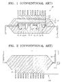
- FIG. 1 is a cross-sectional view of a conventional high power semiconductor package 100 .
- a substrate 40 in the high power semiconductor package 100 can include a base metal layer 10 for transmitting the heat to a heat dissipation plate 80 , a base electrical insulation layer 20 formed on the base metal layer 10 , and a conductive pattern 30 formed on the base insulation layer 20 .
- a high power semiconductor chip 50 a and/or a low power semiconductor chip 50 b can be mounted on the substrate 40 .
- An insulation member 52 for insulating the conductive pattern 30 from the low power semiconductor chip 50 b can be disposed between the conductive pattern 30 and the low power semiconductor chip 50 b.
- Wire bonding pads 51 that are electrically connected to corresponding conductive patterns 30 can be formed on the high power semiconductor chip 50 a and the low power semiconductor chip 50 b.
- the wire bonding pads 51 of the high power semiconductor chip 50 a and the low power semiconductor chip 50 b are electrically connected to the conductive patterns 30 by bonding wires 70 .
- the conductive patterns 30 are connected to leads 60 which form external terminals of the semiconductor package 100 and the high power semiconductor package 100 is completed by performing a transfer molding process using a molding material such as an epoxy molding compound (EMC).
- EMC epoxy molding compound
- the high power semiconductor package 100 generates a lot of heat during operating, and thus, the heat dissipation plate 80 is attached onto the base metal layer 10 .
- the heat dissipation plate 80 is generally formed of a metal having superior thermal conductivity.
- the heat dissipation plate 80 can be attached onto the base metal layer 10 using an attachment member 85 such as a heat-resistant grease.
- FIG. 2 is a schematic side view illustrating a circuit for electrical insulation testing of the high power semiconductor package 100 of FIG. 1 .
- the high power semiconductor chip 50 a operates at the high voltage, for example 600V or higher, in a normal operation mode, and the base electrical insulation layer 20 that insulates the conductive patterns 30 from the base metal layer 10 is required to have high voltage electrical insulating properties. In order to evaluate the insulation property of the base insulation layer 20 , the high power semiconductor package 100 undergoes the electrical insulation tests.
- the electrical insulation test can be performed by checking whether an electric current flows between the heat dissipation plate 80 and the leads 60 while applying a high voltage between the heat dissipation plate 80 and all of the leads 60 that protrude from the semiconductor package 100 .
- the heat-resistant grease 85 is an electrical insulator, the above electrical insulation test cannot reflect the insulation property of the base insulation layer 20 exactly.
- the base metal layer 10 and the heat dissipation plate 80 may sometimes be desirable to electrically connect together the base metal layer 10 and the heat dissipation plate 80 and have the heat dissipation plate 80 grounded in order to provide the high power semiconductor package 100 with an external ground for attenuating electrical noise.
- the package 100 shown in FIG. 1 it may be difficult to provide the base metal layer with the reliable external grounding if the heat-resistant grease 85 has electrical insulating properties.
- the present invention provides a high power semiconductor package that is used with a heat dissipation plate, capable of providing a reliable electrical insulation test and a reliable external ground.
- a high power semiconductor package including: a substrate including a base metal layer, a base insulation layer formed on the base metal layer, and a plurality of conductive patterns formed on the base insulation layer; one or more high power semiconductor chips mounted on the substrate, each including a plurality of bonding pads; one or more first leads having end portions that are electrically connected to the corresponding conductive patterns; and second lead having end portion electrically connected to the base metal layer.
- the bonding pads may be electrically connected to the conductive patterns through first wires.
- the first leads may be connected to the conductive patterns using a soldering process and/or second wires.
- the base insulation layer may include an opening exposing a surface of the base metal layer, and the surface of the base metal layer exposed by the opening may be directly connected to the second lead through a third wire.
- the base insulation layer may include an opening exposing a surface of the base metal layer, the surface of the base metal layer exposed by the opening may be electrically connected to one of the conductive patterns through a third wire, and the second lead may be connected to the conductive pattern that is connected through the third wire using a soldering process.
- the base insulation layer may include an opening exposing a surface of the base metal layer, a connection pad may be formed on the exposed surface of the base metal layer and the second lead may be connected to the connection pad using a soldering.
- the leads electrically connected to the base metal layer are formed, and thus, the insulation property of the base insulation layer in the high power semiconductor package can be tested by performing the processes of the electrical insulation test only between the leads. Accordingly, easy and reliable electrical insulation test processes can be provided according to the present invention.
- independent ground electrodes can be provided by the second leads that are electrically connected to the base metal layer, and thus, an external ground that is more reliable than the conventional ground through the heat-resistant grease can be achieved.
- FIG. 1 is a cross-sectional view of a high power semiconductor package according to the conventional art
- FIG. 2 is a schematic side view of a circuit for electrical insulation testing of the high power semiconductor package of FIG. 1 ;
- FIG. 3 is a cross-sectional side view of a high power semiconductor package according to an embodiment of the present invention.
- FIG. 4 is a cross-sectional plan view of an inner structure of a high power semiconductor package similar to the package shown in FIG. 3 ;
- FIG. 5 is a cross-sectional side view of a high power semiconductor package according to another embodiment of the present invention.
- FIG. 6 is a cross-sectional plan view of an inner structure of a high power semiconductor package similar to the package shown in FIG. 5 .
- first and second etc. are used to denote various members, components, layers, and/or parts, however, the members, components, layers, and/or parts are not limited by the above terms.
- the above terms are used only to distinguish one member, component, region, layer, or part from the other regions, layers, or parts. Therefore, a first member, component, region, layer, or part described hereafter can denote a second member, component, region, layer, or part without departing from teachings of the present invention.
- FIG. 3 is a cross-sectional view of a high power semiconductor package 1000 according to an embodiment of the present invention
- FIG. 4 is a plan view of an inner structure of a high power semiconductor package similar to the package 1000 shown in FIG. 3 .
- a substrate 410 that is, for example, a printed circuit board or a ceramic substrate, includes a base metal layer 110 , a base insulation layer 210 formed on the base metal layer 110 , and conductive patterns 30 formed on the base insulation layer 210 .
- the base metal layer 110 can be formed of a metal material having a high thermal conductivity, such as aluminum or copper.
- the base insulation layer 210 can be formed from a ceramic-based insulation material or a resin-based insulation material.
- a high power semiconductor chip 50 a can be mounted on the conductive pattern 30 providing a drain electrode.
- a low power semiconductor chip 50 b such as a driver integrated circuit (IC) for controlling and driving the high power semiconductor chip 500 a can be mounted on the substrate 410 .
- a smart power module can be constructed.
- An electrical insulation member 52 for insulating the conductive pattern 30 from the low power semiconductor chips 50 b can be disposed between the conductive pattern 30 and the low power semiconductor chip 50 b.
- two or more high power semiconductor chips 50 a and/or two or more low power semiconductor chips 50 b can be stacked on the substrate 400 .
- Wire bonding pads 51 formed on upper portions of the high power semiconductor chips 50 a and/or the low power semiconductor chips 500 b are electrically connected to the conductive patterns 30 through first bonding wires 710 .
- a plurality of leads including leads 600 a and 600 b , provide the package 1000 with external terminals.
- First lead 600 a of the leads 600 a and 600 b may be leads for inputting/outputting signal and/or power, which are electrically connected to bonding pads 51 of the high power semiconductor chip 50 a and the low power semiconductor chip 50 b through the second bonding wire 720 as in a conventional high power semiconductor package 100 described in FIG. 1 .
- Second lead 600 b of the leads 600 a and 600 b may be electrically connected to the base metal layer 110 .
- an opening 200 h exposing a surface of the base metal layer 110 is formed on the base insulation layer 210 , and the surface of the base metal layer 110 exposed by the opening 200 h and the second lead 600 b can be electrically connected directly to the base insulation layer 210 through a third bonding wire 730 .
- the surface of the base metal layer 210 exposed by the opening 200 h is electrically connected to one of the conductive patterns 30 through a third bonding wire 730
- the second lead 600 b is connected to the conductive pattern 30 using a soldering process.
- an expanded contact region 600 be for ensuring an area contacting the bonding wire 730 can be formed on an end portion of the lead 600 b .
- the base insulating layer 210 and the conductive pattern 30 have an opening for the lead 600 b.
- FIGS. 3 and 4 illustrate the leads 600 a and 600 b protruding from both sides of the high power semiconductor packages
- the leads 600 a and 600 b may be formed on only one side or on the bottom side of the high power semiconductor packages.
- the leads 600 a and 600 b may be protruded outwardly from the high power semiconductor package 1000 in various configurations.
- the configuration of the leads 600 a and 600 b does not limit the scope of the present invention.
- a transfer molding process using an EMC is performed to complete the fabrication of the high power semiconductor package 1000 .
- FIG. 5 is a side cross-sectional view of a high power semiconductor package 2010 according to another embodiment of the present invention
- FIG. 6 is a plan cross-sectional view of an inner structure of a high power semiconductor package 2010 similar to the package 2000 of FIG. 5 .
- a high power semiconductor chip 50 a and/or a lower power semiconductor chip 50 b can be mounted on a substrate 420 .
- Two or more high power semiconductor chips 50 a and/or two or more low power semiconductor chips 50 b can be mounted, and can be stacked on the substrate 420 respectively.
- Bonding pads 51 formed on upper portions of the high power semiconductor chip 50 a and/or the low power semiconductor chip 50 b can be electrically connected to conductive patterns 310 through first bonding wires 710 .
- the first lead 600 a may be a lead which is electrically connected to the bonding pads 51 of the high power semiconductor chip 50 a or the low power semiconductor chip 50 b , for inputting/outputting signals or electric power.
- the first lead 600 a can be electrically connected to one of the bonding pads 51 using solder and/or second bonding wires 720 .
- a part of the base insulation layer 220 for example, an edge portion of the base insulation layer 220 , can be removed to expose a surface of the base metal layer 120 .
- a connection pad 640 that can be electrically connected to the second lead 600 b is formed on the exposed surface of the base metal layer 120 , and the second lead 600 b and the connection pad 640 are bonded to each other using, for example, a soldering process or metal bumping process, and thus, the base metal layer 120 can be electrically connected to the second lead 600 b.
- FIGS. 5 and 6 illustrate the leads 600 a and 600 b protruding from both sides of the high power semiconductor packages, however, the leads 600 a and 600 b can be formed only on one side or on the bottom side of the high power semiconductor packages.
- a transfer molding process for injecting an EMC is performed to complete the fabrication of the high power semiconductor package 2000 .
- the second leads 600 b of the embodiments of the present invention can be used as grounding electrodes for attenuating electrical noise.
- some of the conductive patterns 310 that are electrically connected to the semiconductor chips 50 a and 50 b can be connected to the second leads 600 b in order to provide the high power semiconductor package 2010 with common ground electrodes.
- the substrate is not limited to the printed circuit board, and a lead frame that is a support member of the high power semiconductor chip may be used as the substrate of the present invention.
- the leads electrically connected to the base metal layer are formed, and thus, the insulation property of the base insulation layer in the high power semiconductor package can be tested by performing the processes of electrical insulation test only between the leads. Accordingly, an easy and reliable electrical insulation test process can be provided according to the present invention.
- independent ground electrodes can be provided by the leads that are electrically connected to the base metal layer to provide external grounding that is more reliable than the conventional grounding through the heat-resistant grease.
Landscapes
- Cooling Or The Like Of Semiconductors Or Solid State Devices (AREA)
Abstract
Description
Claims (16)
Applications Claiming Priority (2)
| Application Number | Priority Date | Filing Date | Title |
|---|---|---|---|
| KR10-2006-0124110 | 2006-12-07 | ||
| KR1020060124110A KR101194041B1 (en) | 2006-12-07 | 2006-12-07 | High power semiconductor device |
Publications (2)
| Publication Number | Publication Date |
|---|---|
| US20080136015A1 US20080136015A1 (en) | 2008-06-12 |
| US7714428B2 true US7714428B2 (en) | 2010-05-11 |
Family
ID=39497006
Family Applications (1)
| Application Number | Title | Priority Date | Filing Date |
|---|---|---|---|
| US11/951,634 Active 2028-07-23 US7714428B2 (en) | 2006-12-07 | 2007-12-06 | High power semiconductor package and method of making the same |
Country Status (2)
| Country | Link |
|---|---|
| US (1) | US7714428B2 (en) |
| KR (1) | KR101194041B1 (en) |
Cited By (1)
| Publication number | Priority date | Publication date | Assignee | Title |
|---|---|---|---|---|
| US8604610B1 (en) | 2012-06-13 | 2013-12-10 | Fairchild Semiconductor Corporation | Flexible power module semiconductor packages |
Families Citing this family (16)
| Publication number | Priority date | Publication date | Assignee | Title |
|---|---|---|---|---|
| DE102007009341A1 (en) * | 2006-12-21 | 2008-06-26 | Abb Technology Ag | Method and device for optimizing the alarm configuration |
| KR101524545B1 (en) * | 2008-02-28 | 2015-06-01 | 페어차일드코리아반도체 주식회사 | Power device package and the method of fabricating the same |
| KR101519062B1 (en) * | 2008-03-31 | 2015-05-11 | 페어차일드코리아반도체 주식회사 | Semiconductor Device Package |
| JPWO2011018973A1 (en) * | 2009-08-11 | 2013-01-17 | アルプス電気株式会社 | MEMS sensor package |
| KR101826727B1 (en) * | 2011-01-14 | 2018-02-08 | 엘지이노텍 주식회사 | Heat sink and method for manufacturing thereof |
| CN102208403B (en) * | 2011-05-24 | 2013-03-20 | 嘉兴斯达半导体股份有限公司 | Half-bridge power module |
| US20150075849A1 (en) * | 2013-09-17 | 2015-03-19 | Jia Lin Yap | Semiconductor device and lead frame with interposer |
| KR102059610B1 (en) * | 2015-12-18 | 2019-12-26 | 주식회사 엘지화학 | Radiant heating system of printed circuit board using high conductance radiator pad |
| JP6686691B2 (en) * | 2016-05-16 | 2020-04-22 | 株式会社デンソー | Electronic device |
| CN106356345A (en) * | 2016-11-24 | 2017-01-25 | 敦南微电子(无锡)有限公司 | High thermal conductivity high power bridge rectifier structure |
| CN107946272A (en) * | 2017-11-20 | 2018-04-20 | 中航(重庆)微电子有限公司 | A kind of power MOSFET inverter modules of high integration |
| US10957618B2 (en) * | 2018-05-29 | 2021-03-23 | Apex Microtechnology, Inc. | Thermally conductive electronic packaging |
| WO2019234910A1 (en) * | 2018-06-08 | 2019-12-12 | 新電元工業株式会社 | Semiconductor module |
| US20230245942A1 (en) * | 2022-01-31 | 2023-08-03 | Texas Instruments Incorporated | Semiconductor device package with integral heat slug |
| JP7847490B2 (en) * | 2022-06-28 | 2026-04-17 | 三菱電機株式会社 | Power converter |
| KR20240003596A (en) * | 2022-07-01 | 2024-01-09 | 현대자동차주식회사 | Power module |
Citations (6)
| Publication number | Priority date | Publication date | Assignee | Title |
|---|---|---|---|---|
| US5306948A (en) * | 1991-10-03 | 1994-04-26 | Hitachi, Ltd. | Semiconductor device and semiconductor module having auxiliary high power supplying terminals |
| US5471089A (en) | 1992-06-30 | 1995-11-28 | Mitsubishi Denki Kabushiki Kaisha | Semiconductor power module |
| US5513072A (en) | 1993-11-18 | 1996-04-30 | Kabushiki Kaisha Toshiba | Power module using IMS as heat spreader |
| US5519252A (en) | 1992-07-24 | 1996-05-21 | Fuji Electric Co., Ltd. | Power semiconductor device employing pin block connection arrangement for facilitated and economized manufacture |
| US5521437A (en) | 1993-07-05 | 1996-05-28 | Mitsubishi Denki Kabushiki Kaisha | Semiconductor power module having an improved composite board and method of fabricating the same |
| US6002166A (en) | 1996-11-28 | 1999-12-14 | Mitsubishi Denki Kabushiki Kaisha | Semiconductor device |
Family Cites Families (1)
| Publication number | Priority date | Publication date | Assignee | Title |
|---|---|---|---|---|
| US6326678B1 (en) | 1993-09-03 | 2001-12-04 | Asat, Limited | Molded plastic package with heat sink and enhanced electrical performance |
-
2006
- 2006-12-07 KR KR1020060124110A patent/KR101194041B1/en not_active Expired - Fee Related
-
2007
- 2007-12-06 US US11/951,634 patent/US7714428B2/en active Active
Patent Citations (6)
| Publication number | Priority date | Publication date | Assignee | Title |
|---|---|---|---|---|
| US5306948A (en) * | 1991-10-03 | 1994-04-26 | Hitachi, Ltd. | Semiconductor device and semiconductor module having auxiliary high power supplying terminals |
| US5471089A (en) | 1992-06-30 | 1995-11-28 | Mitsubishi Denki Kabushiki Kaisha | Semiconductor power module |
| US5519252A (en) | 1992-07-24 | 1996-05-21 | Fuji Electric Co., Ltd. | Power semiconductor device employing pin block connection arrangement for facilitated and economized manufacture |
| US5521437A (en) | 1993-07-05 | 1996-05-28 | Mitsubishi Denki Kabushiki Kaisha | Semiconductor power module having an improved composite board and method of fabricating the same |
| US5513072A (en) | 1993-11-18 | 1996-04-30 | Kabushiki Kaisha Toshiba | Power module using IMS as heat spreader |
| US6002166A (en) | 1996-11-28 | 1999-12-14 | Mitsubishi Denki Kabushiki Kaisha | Semiconductor device |
Cited By (1)
| Publication number | Priority date | Publication date | Assignee | Title |
|---|---|---|---|---|
| US8604610B1 (en) | 2012-06-13 | 2013-12-10 | Fairchild Semiconductor Corporation | Flexible power module semiconductor packages |
Also Published As
| Publication number | Publication date |
|---|---|
| KR101194041B1 (en) | 2012-10-24 |
| KR20080052081A (en) | 2008-06-11 |
| US20080136015A1 (en) | 2008-06-12 |
Similar Documents
| Publication | Publication Date | Title |
|---|---|---|
| US7714428B2 (en) | High power semiconductor package and method of making the same | |
| US9559068B2 (en) | Wafer scale package for high power devices | |
| US5398160A (en) | Compact power module with a heat spreader | |
| US8796831B2 (en) | Complex semiconductor packages and methods of fabricating the same | |
| US9209114B2 (en) | Power module package with a fastening unit including a non-conductive portion | |
| JP4950280B2 (en) | Low inductance bond wireless joint package for high power density devices, especially for IGBTs and diodes | |
| US9202798B2 (en) | Power module package and method for manufacturing the same | |
| US7709947B2 (en) | Semiconductor device having semiconductor element with back electrode on insulating substrate | |
| US7842545B2 (en) | Semiconductor package having insulated metal substrate and method of fabricating the same | |
| US20140167237A1 (en) | Power module package | |
| US20140110833A1 (en) | Power module package | |
| CN100562999C (en) | Circuit module | |
| JPH1174433A (en) | Semiconductor device | |
| US9655265B2 (en) | Electronic module | |
| US20040245651A1 (en) | Semiconductor device and method for fabricating the same | |
| US6664629B2 (en) | Semiconductor device | |
| US7492038B2 (en) | Semiconductor device | |
| US20250210493A1 (en) | Semiconductor device | |
| JPH077037A (en) | Semiconductor integrated circuit device | |
| CN114556554A (en) | Substrate, packaging structure and electronic equipment | |
| CN114068504A (en) | Semiconductor module | |
| JP2002076258A (en) | Semiconductor device |
Legal Events
| Date | Code | Title | Description |
|---|---|---|---|
| AS | Assignment |
Owner name: FAIRCHILD KOREA SEMICONDUCTOR, LTD., KOREA, DEMOCR Free format text: ASSIGNMENT OF ASSIGNORS INTEREST;ASSIGNORS:LEE, KEUN-HYUK;LIM, SEUNG-WON;REEL/FRAME:020205/0007 Effective date: 20071206 Owner name: FAIRCHILD KOREA SEMICONDUCTOR, LTD.,KOREA, DEMOCRA Free format text: ASSIGNMENT OF ASSIGNORS INTEREST;ASSIGNORS:LEE, KEUN-HYUK;LIM, SEUNG-WON;REEL/FRAME:020205/0007 Effective date: 20071206 |
|
| FEPP | Fee payment procedure |
Free format text: PAYOR NUMBER ASSIGNED (ORIGINAL EVENT CODE: ASPN); ENTITY STATUS OF PATENT OWNER: LARGE ENTITY |
|
| STCF | Information on status: patent grant |
Free format text: PATENTED CASE |
|
| FPAY | Fee payment |
Year of fee payment: 4 |
|
| MAFP | Maintenance fee payment |
Free format text: PAYMENT OF MAINTENANCE FEE, 8TH YEAR, LARGE ENTITY (ORIGINAL EVENT CODE: M1552) Year of fee payment: 8 |
|
| AS | Assignment |
Owner name: SEMICONDUCTOR COMPONENTS INDUSTRIES, LLC, ARIZONA Free format text: ASSIGNMENT OF ASSIGNORS INTEREST;ASSIGNOR:FAIRCHILD KOREA SEMICONDUCTOR, LTD.;REEL/FRAME:044361/0205 Effective date: 20171102 |
|
| AS | Assignment |
Owner name: DEUTSCHE BANK AG NEW YORK BRANCH, AS COLLATERAL AGENT, NEW YORK Free format text: PATENT SECURITY AGREEMENT;ASSIGNORS:SEMICONDUCTOR COMPONENTS INDUSTRIES, LLC;FAIRCHILD SEMICONDUCTOR CORPORATION;REEL/FRAME:044481/0541 Effective date: 20170504 Owner name: DEUTSCHE BANK AG NEW YORK BRANCH, AS COLLATERAL AG Free format text: PATENT SECURITY AGREEMENT;ASSIGNORS:SEMICONDUCTOR COMPONENTS INDUSTRIES, LLC;FAIRCHILD SEMICONDUCTOR CORPORATION;REEL/FRAME:044481/0541 Effective date: 20170504 |
|
| MAFP | Maintenance fee payment |
Free format text: PAYMENT OF MAINTENANCE FEE, 12TH YEAR, LARGE ENTITY (ORIGINAL EVENT CODE: M1553); ENTITY STATUS OF PATENT OWNER: LARGE ENTITY Year of fee payment: 12 |
|
| AS | Assignment |
Owner name: FAIRCHILD SEMICONDUCTOR CORPORATION, ARIZONA Free format text: RELEASE OF SECURITY INTEREST IN PATENTS RECORDED AT REEL 04481, FRAME 0541;ASSIGNOR:DEUTSCHE BANK AG NEW YORK BRANCH, AS COLLATERAL AGENT;REEL/FRAME:064072/0459 Effective date: 20230622 Owner name: SEMICONDUCTOR COMPONENTS INDUSTRIES, LLC, ARIZONA Free format text: RELEASE OF SECURITY INTEREST IN PATENTS RECORDED AT REEL 04481, FRAME 0541;ASSIGNOR:DEUTSCHE BANK AG NEW YORK BRANCH, AS COLLATERAL AGENT;REEL/FRAME:064072/0459 Effective date: 20230622 |