US7714079B2 - Patternable low dielectric constant materials and their use in ULSI interconnection - Google Patents
Patternable low dielectric constant materials and their use in ULSI interconnection Download PDFInfo
- Publication number
- US7714079B2 US7714079B2 US11/933,530 US93353007A US7714079B2 US 7714079 B2 US7714079 B2 US 7714079B2 US 93353007 A US93353007 A US 93353007A US 7714079 B2 US7714079 B2 US 7714079B2
- Authority
- US
- United States
- Prior art keywords
- low
- acid
- film stack
- cured
- sensitive
- Prior art date
- Legal status (The legal status is an assumption and is not a legal conclusion. Google has not performed a legal analysis and makes no representation as to the accuracy of the status listed.)
- Expired - Fee Related
Links
- 0 [1*]C(C)C([2*])C Chemical compound [1*]C(C)C([2*])C 0.000 description 14
- ACEJATUPWDHDTM-UHFFFAOYSA-N C.C.C.C.C.C.C.C.C.C.C.C.C.C.C.C.C.C.C.C.C.C.C.C.C.C.C.C.C.C.C.C.C.C.C.C.CC(C)C(C)C(C(=O)O)C(F)(F)F.CC(C)C(C)c1ccc(O)cc1.CC(C)CCC(C)(O)C(F)(F)F.CC(CC(O)C(F)(F)F)C(C)C(C)c1ccc(O)cc1.CC(CCC(=O)O)C(C)C(C)c1ccc(O)cc1.CC(CCC(=O)OCCO)C(C)CC(C)(O)C(F)(F)F.CC(CCC(C)(O)C(F)(F)F)C(C)CC(O)C(F)(F)F.CC(CCc1ccc(C(C)(O)C(F)(F)F)cc1)C(C)CC(O)C(F)(F)F.CC(CCc1ccc(O)cc1)C(C)CC(O)C(F)(F)F.CC(CO)C(C)CCC(C)(O)C(F)(F)F.OC(CC1CC2CCC1C2)(C(F)(F)F)C(F)(F)F Chemical compound C.C.C.C.C.C.C.C.C.C.C.C.C.C.C.C.C.C.C.C.C.C.C.C.C.C.C.C.C.C.C.C.C.C.C.C.CC(C)C(C)C(C(=O)O)C(F)(F)F.CC(C)C(C)c1ccc(O)cc1.CC(C)CCC(C)(O)C(F)(F)F.CC(CC(O)C(F)(F)F)C(C)C(C)c1ccc(O)cc1.CC(CCC(=O)O)C(C)C(C)c1ccc(O)cc1.CC(CCC(=O)OCCO)C(C)CC(C)(O)C(F)(F)F.CC(CCC(C)(O)C(F)(F)F)C(C)CC(O)C(F)(F)F.CC(CCc1ccc(C(C)(O)C(F)(F)F)cc1)C(C)CC(O)C(F)(F)F.CC(CCc1ccc(O)cc1)C(C)CC(O)C(F)(F)F.CC(CO)C(C)CCC(C)(O)C(F)(F)F.OC(CC1CC2CCC1C2)(C(F)(F)F)C(F)(F)F ACEJATUPWDHDTM-UHFFFAOYSA-N 0.000 description 1
- KZNJUHBCNBUGRL-UHFFFAOYSA-N C=C(C(=O)O)C(F)(F)F.C=C(C(=O)OC)C(F)(F)F.C=C(C(=O)OCCO)C(F)(F)F.C=C(C)C(=O)OC(C)(C)C.C=C(C)C(=O)OCCO.C=C(F)F.C=C(OC(C)(C)C)C(=C)C(F)(F)F.C=CC(=O)OC(C)(C)C.C=CC1CCC(O)CC1.C=CC1CCCC2OC12.C=Cc1ccc(C(C)(O)C(F)(F)F)cc1.C=Cc1ccc(O)cc1.CC(=O)OC(CC1CC2C=CC1C2)(C(F)(F)F)C(F)(F)F.CC(CC1CC2C=CC1C2)(C(F)(F)F)C(F)(F)F.CFF.O=C(O)C1CC2C=CC1C2.O=C1C=CC(=O)O1.OC(CC1CC2C=CC1C2)(C(F)(F)F)C(F)(F)F.OC(F)(C1CC2C=CC1C2)C(F)(F)F Chemical compound C=C(C(=O)O)C(F)(F)F.C=C(C(=O)OC)C(F)(F)F.C=C(C(=O)OCCO)C(F)(F)F.C=C(C)C(=O)OC(C)(C)C.C=C(C)C(=O)OCCO.C=C(F)F.C=C(OC(C)(C)C)C(=C)C(F)(F)F.C=CC(=O)OC(C)(C)C.C=CC1CCC(O)CC1.C=CC1CCCC2OC12.C=Cc1ccc(C(C)(O)C(F)(F)F)cc1.C=Cc1ccc(O)cc1.CC(=O)OC(CC1CC2C=CC1C2)(C(F)(F)F)C(F)(F)F.CC(CC1CC2C=CC1C2)(C(F)(F)F)C(F)(F)F.CFF.O=C(O)C1CC2C=CC1C2.O=C1C=CC(=O)O1.OC(CC1CC2C=CC1C2)(C(F)(F)F)C(F)(F)F.OC(F)(C1CC2C=CC1C2)C(F)(F)F KZNJUHBCNBUGRL-UHFFFAOYSA-N 0.000 description 1
- DLMCKMKXLVMIGN-UHFFFAOYSA-N CC(=O)C1CC2CC(C)C1C2.CC(C)C1=CC=C(C(O)(C(F)(F)F)C(F)(F)F)C=C1.CC(C)C1=CC=C(O)C=C1.CC1CC2CC(CC(O)(C(F)(F)F)C(F)(F)F)C1C2.CC1CC2CC1C(C(O)(C(F)(F)F)C(F)(F)F)C2.CCC(C(=O)O)C(F)(F)F.CCC(C)C(=O)O.CCC(O)(C(F)(F)F)C(F)(F)F.CCC(O)C(F)(F)F.CCC1=CC=C(CC(O)(F)C(F)(F)F)C=C1.CCC1=CC=C(O)C=C1.CCCC(=O)O.CCCC(=O)OC(C1CCC(C(O)(C(F)(F)F)C(F)(F)F)CC1)(C(F)(F)F)C(F)(F)F.CCCC(O)(C(F)(F)F)C(F)(F)F.CCCC1=CC=C(C(O)(C(F)(F)F)C(F)(F)F)C=C1.CCCC1=CC=C(CC(O)(F)C(F)(F)F)C=C1.CCCC1=CC=C(O)C=C1.CFF.CFF Chemical compound CC(=O)C1CC2CC(C)C1C2.CC(C)C1=CC=C(C(O)(C(F)(F)F)C(F)(F)F)C=C1.CC(C)C1=CC=C(O)C=C1.CC1CC2CC(CC(O)(C(F)(F)F)C(F)(F)F)C1C2.CC1CC2CC1C(C(O)(C(F)(F)F)C(F)(F)F)C2.CCC(C(=O)O)C(F)(F)F.CCC(C)C(=O)O.CCC(O)(C(F)(F)F)C(F)(F)F.CCC(O)C(F)(F)F.CCC1=CC=C(CC(O)(F)C(F)(F)F)C=C1.CCC1=CC=C(O)C=C1.CCCC(=O)O.CCCC(=O)OC(C1CCC(C(O)(C(F)(F)F)C(F)(F)F)CC1)(C(F)(F)F)C(F)(F)F.CCCC(O)(C(F)(F)F)C(F)(F)F.CCCC1=CC=C(C(O)(C(F)(F)F)C(F)(F)F)C=C1.CCCC1=CC=C(CC(O)(F)C(F)(F)F)C=C1.CCCC1=CC=C(O)C=C1.CFF.CFF DLMCKMKXLVMIGN-UHFFFAOYSA-N 0.000 description 1
- BSAMIHNJQILJIF-UHFFFAOYSA-N CC(C)C1=CC=C(CC(O)(C(F)(F)F)C(F)(F)F)C=C1.CCC1=CC=C(CC(O)(C(F)(F)F)C(F)(F)F)C=C1.CCCC1=CC=C(CC(O)(C(F)(F)F)C(F)(F)F)C=C1.CCCC1=CC=C(O)C=C1 Chemical compound CC(C)C1=CC=C(CC(O)(C(F)(F)F)C(F)(F)F)C=C1.CCC1=CC=C(CC(O)(C(F)(F)F)C(F)(F)F)C=C1.CCCC1=CC=C(CC(O)(C(F)(F)F)C(F)(F)F)C=C1.CCCC1=CC=C(O)C=C1 BSAMIHNJQILJIF-UHFFFAOYSA-N 0.000 description 1
- ZWWLGVPFHQMJEH-UHFFFAOYSA-N CC.CC(C)C1=CC=C(C(O)(C(F)(F)F)C(F)(F)F)C=C1.CC(C)C1=CC=C(O)C=C1.CC1CC2CC(C(=O)O)C1C2.CC1CC2CC(CC(O)(C(F)(F)F)C(F)(F)F)C1C2.CCC(C(=O)O)C(F)(F)F.CCC(C)C(=O)O.CCC(O)(C(F)(F)F)C(F)(F)F.CCC(O)C(F)(F)F.CCC1=CC=C(CC(O)(F)C(F)(F)F)C=C1.CCC1=CC=C(O)C=C1.CCCC(=O)O.CCCC(=O)OC(C1CCC(C(O)(C(F)(F)F)C(F)(F)F)CC1)(C(F)(F)F)C(F)(F)F.CCCC(O)(C(F)(F)F)C(F)(F)F.CCCC1=CC=C(C(O)(C(F)(F)F)C(F)(F)F)C=C1.CCCC1=CC=C(CC(O)(F)C(F)(F)F)C=C1.CCCC1=CC=C(O)C=C1.CFF.CFF.OC(C1CC2CCC1C2)(C(F)(F)F)C(F)(F)F Chemical compound CC.CC(C)C1=CC=C(C(O)(C(F)(F)F)C(F)(F)F)C=C1.CC(C)C1=CC=C(O)C=C1.CC1CC2CC(C(=O)O)C1C2.CC1CC2CC(CC(O)(C(F)(F)F)C(F)(F)F)C1C2.CCC(C(=O)O)C(F)(F)F.CCC(C)C(=O)O.CCC(O)(C(F)(F)F)C(F)(F)F.CCC(O)C(F)(F)F.CCC1=CC=C(CC(O)(F)C(F)(F)F)C=C1.CCC1=CC=C(O)C=C1.CCCC(=O)O.CCCC(=O)OC(C1CCC(C(O)(C(F)(F)F)C(F)(F)F)CC1)(C(F)(F)F)C(F)(F)F.CCCC(O)(C(F)(F)F)C(F)(F)F.CCCC1=CC=C(C(O)(C(F)(F)F)C(F)(F)F)C=C1.CCCC1=CC=C(CC(O)(F)C(F)(F)F)C=C1.CCCC1=CC=C(O)C=C1.CFF.CFF.OC(C1CC2CCC1C2)(C(F)(F)F)C(F)(F)F ZWWLGVPFHQMJEH-UHFFFAOYSA-N 0.000 description 1
- WQMWMGDLFFBWFB-UHFFFAOYSA-N CCC(C(=O)OC(C)(C)C)C(F)(F)F.CCC(C)C(=O)OC(C)(C)C.CCCC(=O)OC(C)(C)C.CO[Si](C)(C)C(C)c1ccc(OC(=O)OC(C)(C)C)cc1.CO[Si](C)(C)C1CC2CC1CC2C(O)(C(F)(F)F)C(F)(F)F.CO[Si](C)(C)CCc1ccc(O)cc1 Chemical compound CCC(C(=O)OC(C)(C)C)C(F)(F)F.CCC(C)C(=O)OC(C)(C)C.CCCC(=O)OC(C)(C)C.CO[Si](C)(C)C(C)c1ccc(OC(=O)OC(C)(C)C)cc1.CO[Si](C)(C)C1CC2CC1CC2C(O)(C(F)(F)F)C(F)(F)F.CO[Si](C)(C)CCc1ccc(O)cc1 WQMWMGDLFFBWFB-UHFFFAOYSA-N 0.000 description 1
- UJBRYIQCSKHHHY-UHFFFAOYSA-N COCN(CC1=NC(N(COC)COC)=NC(N(COC)COC)=N1)OC.COCN1CCCN(COC)C1=O.COCN1CN(C)CN(COC)C1=O.COCN1COCN(COC)C1=O.[H]CC1=NC(N(C[H])OC)=NC(NCOC)=N1 Chemical compound COCN(CC1=NC(N(COC)COC)=NC(N(COC)COC)=N1)OC.COCN1CCCN(COC)C1=O.COCN1CN(C)CN(COC)C1=O.COCN1COCN(COC)C1=O.[H]CC1=NC(N(C[H])OC)=NC(NCOC)=N1 UJBRYIQCSKHHHY-UHFFFAOYSA-N 0.000 description 1
- GNBCQANWHPNGBC-UHFFFAOYSA-N CO[N]1(N)O[N](N)(ON(N)ON(N)OI)ON(N)ON(N)O1 Chemical compound CO[N]1(N)O[N](N)(ON(N)ON(N)OI)ON(N)ON(N)O1 GNBCQANWHPNGBC-UHFFFAOYSA-N 0.000 description 1
Images


Classifications
-
- G—PHYSICS
- G03—PHOTOGRAPHY; CINEMATOGRAPHY; ANALOGOUS TECHNIQUES USING WAVES OTHER THAN OPTICAL WAVES; ELECTROGRAPHY; HOLOGRAPHY
- G03F—PHOTOMECHANICAL PRODUCTION OF TEXTURED OR PATTERNED SURFACES, e.g. FOR PRINTING, FOR PROCESSING OF SEMICONDUCTOR DEVICES; MATERIALS THEREFOR; ORIGINALS THEREFOR; APPARATUS SPECIALLY ADAPTED THEREFOR
- G03F7/00—Photomechanical, e.g. photolithographic, production of textured or patterned surfaces, e.g. printing surfaces; Materials therefor, e.g. comprising photoresists; Apparatus specially adapted therefor
- G03F7/004—Photosensitive materials
- G03F7/075—Silicon-containing compounds
- G03F7/0757—Macromolecular compounds containing Si-O, Si-C or Si-N bonds
-
- G—PHYSICS
- G03—PHOTOGRAPHY; CINEMATOGRAPHY; ANALOGOUS TECHNIQUES USING WAVES OTHER THAN OPTICAL WAVES; ELECTROGRAPHY; HOLOGRAPHY
- G03F—PHOTOMECHANICAL PRODUCTION OF TEXTURED OR PATTERNED SURFACES, e.g. FOR PRINTING, FOR PROCESSING OF SEMICONDUCTOR DEVICES; MATERIALS THEREFOR; ORIGINALS THEREFOR; APPARATUS SPECIALLY ADAPTED THEREFOR
- G03F7/00—Photomechanical, e.g. photolithographic, production of textured or patterned surfaces, e.g. printing surfaces; Materials therefor, e.g. comprising photoresists; Apparatus specially adapted therefor
- G03F7/004—Photosensitive materials
- G03F7/075—Silicon-containing compounds
-
- C—CHEMISTRY; METALLURGY
- C08—ORGANIC MACROMOLECULAR COMPOUNDS; THEIR PREPARATION OR CHEMICAL WORKING-UP; COMPOSITIONS BASED THEREON
- C08G—MACROMOLECULAR COMPOUNDS OBTAINED OTHERWISE THAN BY REACTIONS ONLY INVOLVING UNSATURATED CARBON-TO-CARBON BONDS
- C08G77/00—Macromolecular compounds obtained by reactions forming a linkage containing silicon with or without sulfur, nitrogen, oxygen or carbon in the main chain of the macromolecule
- C08G77/04—Polysiloxanes
- C08G77/22—Polysiloxanes containing silicon bound to organic groups containing atoms other than carbon, hydrogen and oxygen
- C08G77/24—Polysiloxanes containing silicon bound to organic groups containing atoms other than carbon, hydrogen and oxygen halogen-containing groups
-
- C—CHEMISTRY; METALLURGY
- C09—DYES; PAINTS; POLISHES; NATURAL RESINS; ADHESIVES; COMPOSITIONS NOT OTHERWISE PROVIDED FOR; APPLICATIONS OF MATERIALS NOT OTHERWISE PROVIDED FOR
- C09D—COATING COMPOSITIONS, e.g. PAINTS, VARNISHES OR LACQUERS; FILLING PASTES; CHEMICAL PAINT OR INK REMOVERS; INKS; CORRECTING FLUIDS; WOODSTAINS; PASTES OR SOLIDS FOR COLOURING OR PRINTING; USE OF MATERIALS THEREFOR
- C09D183/00—Coating compositions based on macromolecular compounds obtained by reactions forming in the main chain of the macromolecule a linkage containing silicon, with or without sulfur, nitrogen, oxygen, or carbon only; Coating compositions based on derivatives of such polymers
- C09D183/04—Polysiloxanes
- C09D183/08—Polysiloxanes containing silicon bound to organic groups containing atoms other than carbon, hydrogen, and oxygen
-
- G—PHYSICS
- G03—PHOTOGRAPHY; CINEMATOGRAPHY; ANALOGOUS TECHNIQUES USING WAVES OTHER THAN OPTICAL WAVES; ELECTROGRAPHY; HOLOGRAPHY
- G03F—PHOTOMECHANICAL PRODUCTION OF TEXTURED OR PATTERNED SURFACES, e.g. FOR PRINTING, FOR PROCESSING OF SEMICONDUCTOR DEVICES; MATERIALS THEREFOR; ORIGINALS THEREFOR; APPARATUS SPECIALLY ADAPTED THEREFOR
- G03F7/00—Photomechanical, e.g. photolithographic, production of textured or patterned surfaces, e.g. printing surfaces; Materials therefor, e.g. comprising photoresists; Apparatus specially adapted therefor
- G03F7/004—Photosensitive materials
- G03F7/0046—Photosensitive materials with perfluoro compounds, e.g. for dry lithography
-
- H—ELECTRICITY
- H10—SEMICONDUCTOR DEVICES; ELECTRIC SOLID-STATE DEVICES NOT OTHERWISE PROVIDED FOR
- H10P—GENERIC PROCESSES OR APPARATUS FOR THE MANUFACTURE OR TREATMENT OF DEVICES COVERED BY CLASS H10
- H10P14/00—Formation of materials, e.g. in the shape of layers or pillars
- H10P14/60—Formation of materials, e.g. in the shape of layers or pillars of insulating materials
- H10P14/65—Formation of materials, e.g. in the shape of layers or pillars of insulating materials characterised by treatments performed before or after the formation of the materials
- H10P14/6516—Formation of materials, e.g. in the shape of layers or pillars of insulating materials characterised by treatments performed before or after the formation of the materials of treatments performed after formation of the materials
- H10P14/6536—Formation of materials, e.g. in the shape of layers or pillars of insulating materials characterised by treatments performed before or after the formation of the materials of treatments performed after formation of the materials by exposure to radiation, e.g. visible light
- H10P14/6538—Formation of materials, e.g. in the shape of layers or pillars of insulating materials characterised by treatments performed before or after the formation of the materials of treatments performed after formation of the materials by exposure to radiation, e.g. visible light by exposure to UV light
-
- H—ELECTRICITY
- H10—SEMICONDUCTOR DEVICES; ELECTRIC SOLID-STATE DEVICES NOT OTHERWISE PROVIDED FOR
- H10P—GENERIC PROCESSES OR APPARATUS FOR THE MANUFACTURE OR TREATMENT OF DEVICES COVERED BY CLASS H10
- H10P14/00—Formation of materials, e.g. in the shape of layers or pillars
- H10P14/60—Formation of materials, e.g. in the shape of layers or pillars of insulating materials
- H10P14/68—Organic materials, e.g. photoresists
- H10P14/683—Organic materials, e.g. photoresists carbon-based polymeric organic materials, e.g. polyimides, poly cyclobutene or PVC
-
- H—ELECTRICITY
- H10—SEMICONDUCTOR DEVICES; ELECTRIC SOLID-STATE DEVICES NOT OTHERWISE PROVIDED FOR
- H10W—GENERIC PACKAGES, INTERCONNECTIONS, CONNECTORS OR OTHER CONSTRUCTIONAL DETAILS OF DEVICES COVERED BY CLASS H10
- H10W20/00—Interconnections in chips, wafers or substrates
- H10W20/01—Manufacture or treatment
- H10W20/071—Manufacture or treatment of dielectric parts thereof
- H10W20/072—Manufacture or treatment of dielectric parts thereof of dielectric parts comprising air gaps
-
- H—ELECTRICITY
- H10—SEMICONDUCTOR DEVICES; ELECTRIC SOLID-STATE DEVICES NOT OTHERWISE PROVIDED FOR
- H10W—GENERIC PACKAGES, INTERCONNECTIONS, CONNECTORS OR OTHER CONSTRUCTIONAL DETAILS OF DEVICES COVERED BY CLASS H10
- H10W20/00—Interconnections in chips, wafers or substrates
- H10W20/01—Manufacture or treatment
- H10W20/071—Manufacture or treatment of dielectric parts thereof
- H10W20/081—Manufacture or treatment of dielectric parts thereof by forming openings in the dielectric parts
-
- H—ELECTRICITY
- H10—SEMICONDUCTOR DEVICES; ELECTRIC SOLID-STATE DEVICES NOT OTHERWISE PROVIDED FOR
- H10W—GENERIC PACKAGES, INTERCONNECTIONS, CONNECTORS OR OTHER CONSTRUCTIONAL DETAILS OF DEVICES COVERED BY CLASS H10
- H10W20/00—Interconnections in chips, wafers or substrates
- H10W20/40—Interconnections external to wafers or substrates, e.g. back-end-of-line [BEOL] metallisations or vias connecting to gate electrodes
- H10W20/45—Interconnections external to wafers or substrates, e.g. back-end-of-line [BEOL] metallisations or vias connecting to gate electrodes characterised by their insulating parts
- H10W20/46—Interconnections external to wafers or substrates, e.g. back-end-of-line [BEOL] metallisations or vias connecting to gate electrodes characterised by their insulating parts comprising air gaps
-
- H—ELECTRICITY
- H10—SEMICONDUCTOR DEVICES; ELECTRIC SOLID-STATE DEVICES NOT OTHERWISE PROVIDED FOR
- H10W—GENERIC PACKAGES, INTERCONNECTIONS, CONNECTORS OR OTHER CONSTRUCTIONAL DETAILS OF DEVICES COVERED BY CLASS H10
- H10W20/00—Interconnections in chips, wafers or substrates
- H10W20/40—Interconnections external to wafers or substrates, e.g. back-end-of-line [BEOL] metallisations or vias connecting to gate electrodes
- H10W20/45—Interconnections external to wafers or substrates, e.g. back-end-of-line [BEOL] metallisations or vias connecting to gate electrodes characterised by their insulating parts
- H10W20/48—Insulating materials thereof
-
- H—ELECTRICITY
- H10—SEMICONDUCTOR DEVICES; ELECTRIC SOLID-STATE DEVICES NOT OTHERWISE PROVIDED FOR
- H10P—GENERIC PROCESSES OR APPARATUS FOR THE MANUFACTURE OR TREATMENT OF DEVICES COVERED BY CLASS H10
- H10P14/00—Formation of materials, e.g. in the shape of layers or pillars
- H10P14/60—Formation of materials, e.g. in the shape of layers or pillars of insulating materials
- H10P14/63—Formation of materials, e.g. in the shape of layers or pillars of insulating materials characterised by the formation processes
- H10P14/6326—Deposition processes
- H10P14/6342—Liquid deposition, e.g. spin-coating, sol-gel techniques or spray coating
-
- H—ELECTRICITY
- H10—SEMICONDUCTOR DEVICES; ELECTRIC SOLID-STATE DEVICES NOT OTHERWISE PROVIDED FOR
- H10P—GENERIC PROCESSES OR APPARATUS FOR THE MANUFACTURE OR TREATMENT OF DEVICES COVERED BY CLASS H10
- H10P14/00—Formation of materials, e.g. in the shape of layers or pillars
- H10P14/60—Formation of materials, e.g. in the shape of layers or pillars of insulating materials
- H10P14/66—Formation of materials, e.g. in the shape of layers or pillars of insulating materials characterised by the type of materials
- H10P14/665—Porous materials
-
- H—ELECTRICITY
- H10—SEMICONDUCTOR DEVICES; ELECTRIC SOLID-STATE DEVICES NOT OTHERWISE PROVIDED FOR
- H10P—GENERIC PROCESSES OR APPARATUS FOR THE MANUFACTURE OR TREATMENT OF DEVICES COVERED BY CLASS H10
- H10P14/00—Formation of materials, e.g. in the shape of layers or pillars
- H10P14/60—Formation of materials, e.g. in the shape of layers or pillars of insulating materials
- H10P14/66—Formation of materials, e.g. in the shape of layers or pillars of insulating materials characterised by the type of materials
- H10P14/668—Formation of materials, e.g. in the shape of layers or pillars of insulating materials characterised by the type of materials the materials being characterised by the deposition precursor materials
- H10P14/6681—Formation of materials, e.g. in the shape of layers or pillars of insulating materials characterised by the type of materials the materials being characterised by the deposition precursor materials the precursor containing a compound comprising Si
- H10P14/6684—Formation of materials, e.g. in the shape of layers or pillars of insulating materials characterised by the type of materials the materials being characterised by the deposition precursor materials the precursor containing a compound comprising Si the compound comprising silicon and oxygen
- H10P14/6686—Formation of materials, e.g. in the shape of layers or pillars of insulating materials characterised by the type of materials the materials being characterised by the deposition precursor materials the precursor containing a compound comprising Si the compound comprising silicon and oxygen the compound being a molecule comprising at least one silicon-oxygen bond and the compound having hydrogen or an organic group attached to the silicon or oxygen, e.g. a siloxane
-
- H—ELECTRICITY
- H10—SEMICONDUCTOR DEVICES; ELECTRIC SOLID-STATE DEVICES NOT OTHERWISE PROVIDED FOR
- H10P—GENERIC PROCESSES OR APPARATUS FOR THE MANUFACTURE OR TREATMENT OF DEVICES COVERED BY CLASS H10
- H10P14/00—Formation of materials, e.g. in the shape of layers or pillars
- H10P14/60—Formation of materials, e.g. in the shape of layers or pillars of insulating materials
- H10P14/69—Inorganic materials
- H10P14/692—Inorganic materials composed of oxides, glassy oxides or oxide-based glasses
- H10P14/6921—Inorganic materials composed of oxides, glassy oxides or oxide-based glasses containing silicon
- H10P14/6922—Inorganic materials composed of oxides, glassy oxides or oxide-based glasses containing silicon the material containing Si, O and at least one of H, N, C, F or other non-metal elements, e.g. SiOC, SiOC:H or SiONC
-
- Y—GENERAL TAGGING OF NEW TECHNOLOGICAL DEVELOPMENTS; GENERAL TAGGING OF CROSS-SECTIONAL TECHNOLOGIES SPANNING OVER SEVERAL SECTIONS OF THE IPC; TECHNICAL SUBJECTS COVERED BY FORMER USPC CROSS-REFERENCE ART COLLECTIONS [XRACs] AND DIGESTS
- Y10—TECHNICAL SUBJECTS COVERED BY FORMER USPC
- Y10T—TECHNICAL SUBJECTS COVERED BY FORMER US CLASSIFICATION
- Y10T428/00—Stock material or miscellaneous articles
- Y10T428/31504—Composite [nonstructural laminate]
- Y10T428/31652—Of asbestos
- Y10T428/31663—As siloxane, silicone or silane
Definitions
- the present invention relates to ultra-large scale integrated (ULSI) interconnect structures, and more particularly to patternable low dielectric constant (low-k) materials suitable for use in ULSI interconnect structures.
- the patternable low-k dielectrics disclosed herein comprise a functionalized polymer having one or more acid-sensitive imageable functional groups. More specifically, the patternable low-k dielectrics of the present invention are based on acid-catalyzed photochemical transformation of silsesquioxane (SSQ)-type polymers under irradiation to achieve patterning capability which are then converted into a low-k material after curing.
- SSQ silsesquioxane
- the present invention also provides a method of integrating the patternable low-k materials of the present invention in semiconductor back-end-of-the-line (BEOL) structures.
- semiconductor devices include a plurality of integrated circuits (ICs).
- ICs can be useful for many applications including computers and electronic equipment and they can contain millions of transistors and other circuit elements that can be fabricated on a single semiconductor chip.
- ICs can be useful for many applications including computers and electronic equipment and they can contain millions of transistors and other circuit elements that can be fabricated on a single semiconductor chip.
- a complex of signal paths will typically be routed to connect the circuit elements distributed on the surface of the semiconductor device. Efficient routing of these signals across the device can become more difficult as the complexity and number of ICs is increased.
- the formation of multi-level or multi-layered interconnect schemes, including dual damascene has become more desirable due to their efficacy in providing high-speed signal routing patterns between a large number of transistors on a single semiconductor chip.
- an electrically insulating material (oftentimes referred to as a dielectric material) such as SiO 2 , will normally be patterned to create openings for conductive lines and/or vias using photolithography and etching. These openings formed into the dielectric material are typically filled with a conductive material such as Cu or Al to interconnect the active device regions of the ICs. After the filling process, the semiconductor device is generally planarized by chemical-mechanical polishing. Interconnect structures of the dual damascene type are highly preferred in the industry.
- the patterning of conventional insulating materials such as SiO 2 includes the use of many layers of different patterning and masking materials (typically up to 7 different layers of materials are employed in the prior art) that are formed atop the insulating layer prior to patterning.
- a nitride hard mask, a silicon oxide hard mask, and a metal hard mask may all be used in patterning a single insulating layer of a typical interconnect structure.
- a photoresist and an anti-reflective coating are generally applied to the uppermost surface of the masking layers.
- the photoresist is then patterned by lithography and thereafter a series of etching steps are employed to first transfer the pattern from the photoresist to each of the masking layers and thereafter to the insulating layer. Furthermore, these masking layers have to be removed after patterning. Therefore, the prior art process of patterning a dielectric material is a very inefficient process.
- low-k denotes a dielectric material that has a dielectric constant lower than SiO 2 , i.e., ⁇ 3.9.
- various polymer dielectrics such as polyarylenes and carbon-doped organosilicates have been developed and are currently being integrated into various IC interconnect structures. These low-k dielectrics are particularly advantageous for use as an interconnect dielectric because they significantly reduce signal delay and cross-talk in interconnect structures due to their lower dielectric constant.
- prior art low-k dielectrics are typically photoinactive; therefore the patterning thereof requires the above mentioned multilayer masking scheme.
- Prior art multilayer masking schemes of the type mentioned above are extremely insufficient because: (i) they need many layers of sacrificial materials; (ii) each individual masking layer needs to be removed after patterning; (iii) the various masking layers sometimes increase the effective dielectric constant of the IC; and (iv) they increase integration complexity and manufacturing costs (i.e., a need for separate and expensive deposition and etching tools).
- a separate photoresist is typically needed to pattern the same.
- the patterning of prior art photoinactive low-k materials requires first patterning of the photoresist and thereafter various etching steps which transfer the pattern from the photoresist into each of the masking layers before ultimately patterning of the low-k dielectric.
- silsesquioxane polymers containing base sensitive functional groups are known. See, for example, U.S. Pat. Nos. 5,789,460 to Harkness, et al.; U.S. Pat. No. 5,891,529 to Harkness, et al.; U.S. Pat. No. 5,820,944, to Harkness, et al.; U.S. Pat. No. 5,861,235 to Harkness, et al.; U.S. Pat. No. 6,096,483 to Harkness, et al.; U.S. Pat. No. 6,051,625 to Harkness, et al.; and U.S. Pat. No.
- a low-k dielectric material that can be used as an inter-level or intra-level dielectric of an interconnect structure, yet does not require numerous materials (i.e., masking layers, photoresist and ARC) and processing steps for patterning the same. That is, a material is needed which combines the functions of a photoresist and a conventional low-k dielectric into a single material. Such a material would greatly reduce the integration complexity and processing steps required in the prior art to provide a patterned low-k interconnect dielectric. Separate photoresist (or masking layers) and related patterning processes (deposition and etching tools) would not be needed since the material would be capable of being patterned itself.
- the present invention provides a composition of matter which includes a functionalized polymer having one or more acid-sensitive imageable groups.
- the polymers employed in the present invention are low-k polymers or polymers that can be converted into low-k polymers after subsequent processing, either by heat or light. More specifically, the polymers employed in the present invention include, but are not limited to: hydrocarbons, fluorinated hydrocarbons, organosilicates, silsesquioxanes and the like. Of these polymers, silsesquioxane-type polymers including caged, linear, branched or combinations thereof; are preferred, with caged silsesquioxane polymers being more highly preferred.
- the present invention also provides a method for synthesizing the caged silsesquioxane polymers.
- the term “acid-sensitive” is used throughout the application to denote imageable functional groups which undergo a chemical reaction in the presence of an acid generated by a photoacid generator under exposure to radiation.
- the acid-sensitive imageable functional groups employed in the present invention may include acid-sensitive positive-tone functional groups or acid-sensitive negative-tone functional groups.
- the negative-tone acid-sensitive functional groups are functional groups for causing a crosslinking reaction which causes the exposed areas to be insoluble in a developer to form a negative-tone relief images after development.
- the positive-tone acid-sensitive functional groups are acid-sensitive protecting groups which cause the exposed region to be soluble in a developer to form positive-tone relief images after development. In the present invention, acid-sensitive negative-tone functional groups are preferred.
- crosslinking functional groups include OH, epoxy, branched alcohols and SiH
- acid-sensitive protecting groups include high activation energy protecting groups such as branched alkyl tertiary ester groups, branched alkyl carbonyl groups and mixtures thereof, and low activation energy protecting groups such as tertiary acetals, tertiary ketals or tertiary silylethers.
- the present invention also provides a patternable low-k composition which includes at least the composition of matter of the present invention, e.g., a functionalized polymer containing one or more acid-sensitive imageable functional groups.
- the patternable low-k composition of the present invention may be used in conjunction with at least an acid generator and/or a crosslinking agent.
- a solvent is also present in the patternable low-k composition of the present invention.
- Optional ingredients include, a base and a surfactant.
- the patternable low-k composition of the present invention is patterned by standard lithography processes or contacting printing processes and is converted into a low-k dielectric material by curing the same.
- a pore-generating compound called a porogen
- a porogen is incorporated into the composition of matter, including the patternable low-k composition of the present invention.
- the porogen provides nanoscopic pores in the composition of matter of the present invention which further reduces the dielectric constant of the material.
- the porogen that can be used in the present invention includes miscible or phase separated, i.e., non-miscible, polymers that are capable of decomposing under heat or radiation.
- the porogen may be extracted with supercritical fluid techniques.
- porogens that may be employed in the present invention include: homopolymers, copolymers, organic nanoscopic polymers, thermoplatic polymers, star-shaped polymers, dendrimers or crosslinked polymers that remain substantially dormant during the patterning process.
- the pore generating polymers are decomposed or extracted to enhance the dielectric properties of the material of the present invention without severely degrading the pattern fidelity.
- the decomposition of the porogen may be by heat or radiation-induced.
- composition of matter of the present invention may also include a non-silsesquioxane containing compound.
- inventive patternable low-k dielectric composition and material of the present invention can be used in standard single or dual damascene interconnect structures or etch back/gap fill and air bridge integration schemes.
- the present invention also provides a method of forming an interconnect structure, particularly a dual damascene interconnect structure, which includes at least the patternable low-k dielectric material of the present invention as an inter-level and/or intra-level dielectric material.
- the present invention also provides a film stack which includes a substrate, the patternable low-k material of the present invention, after coating and curing, atop the substrate, and an overlying layer located on the patternable low-k material.
- the patternable low-k material of the present invention preferably includes a conductive metal, such as Cu or Al, embedded therein.
- patternable low-k composition denotes the inventive composition of matter prior to curing
- patternable low-k material denotes the material that is formed after curing
- the patternable low-k dielectric material of the present invention offers several advantages over the state-of-the-art low-k materials including, for example:
- the patternable low-k dielectrics of the present invention combine the functions of a photoresist and a traditional low-k dielectric material into a single material. Therefore, patterning of the dielectric of the present invention can be accomplished on the dielectric itself. No separate photoresist and related processes (i.e., separate deposition and etching tools) are needed. This simplification greatly reduces the processing steps and costs required in the integration of low-k materials.
- highly-sensitive and high-resolution photo-patterned low-k materials can be obtained. Since the present invention utilizes a chemical amplification concept and polymers that are optical transparent to short wavelengths, patternable low-k materials suitable for 400 nm and below optical lithography, including I-line, 248 nm, 193 nm, 157 nm, EUV (13.4 nm) lithography, e-beam, and other lithography's are provided herein.
- the present invention significantly reduces the processing steps in the integration of low-k dielectric materials by combining the functions of two separate and distinct materials into a single material. This is accomplished in the present invention by functionalizing a polymer with acid-sensitive imageable groups.
- low-k as used throughout the remaining portions of the present application denotes a dielectric material having a dielectric constant of less than 3.9, preferably less than 3.0.
- FIGS. 1A and 1B are schematic diagrams showing methods for synthesizing caged silsesquioxane polymers according to a preferred embodiment of the present invention.
- FIGS. 2A-2D are pictorial representations (though cross-sectional views) illustrating the use of the patternable low-k dielectric material of the present invention as an interconnect dielectric in dual damascene interconnects.
- the present invention provides a composition of matter that comprises a functionalized polymer having one or more acid-sensitive imageable functional groups.
- the polymer employed in the present invention includes hydrocarbons, fluorinated hydrocarbons, organosilicates, silsesquioxanes, and other like polymers that have a low-k or can be converted into a low-k material upon further treatment.
- silsesquioxane-type polymers including caged, linear, branched, or combinations thereof are preferred, with caged silsesquioxane polymers being more highly preferred.
- the functionalized polymer, particularly the positive-tone polymer is made by well-known techniques which include the addition of the one or more acid-sensitive imageable functional groups to the polymer.
- the acid-sensitive imageable functional groups employed in the present invention may include acid-sensitive positive-tone functional groups or acid-sensitive negative-tone functional groups.
- the negative-tone functional groups are functional groups for causing a crosslinking reaction (crosslinking can be effected by the functional group itself or by a crosslinking agent), while the positive-tone functional groups are acid-sensitive protecting groups.
- crosslinking can be effected by the functional group itself or by a crosslinking agent
- the positive-tone functional groups are acid-sensitive protecting groups.
- a photo-chemically generated acid catalyzes the crosslinking of the functional groups, either with or without an additional agent, to render the exposed area insoluble in a developer. Subsequently development with a proper developer generates negative-tone relief images.
- a photo-chemically generated acid catalyzes the deprotection of the acid sensitive protecting functional groups to render the exposed area soluble in a developer. Subsequently development with a proper developer generates positive-tone relief images.
- crosslinking functional groups include OH, epoxy, branched alcohols and SiH
- acid-sensitive protecting groups include high activation energy protecting groups such as branched alkyl tertiary ester groups, branched alkyl carbonyl groups and mixtures thereof, and low activation energy protecting groups such as tertiary acetals, tertiary ketals or tertiary silylethers.
- the silsesquioxane polymer is a linear, branched, caged compound or combination thereof having the following structural formula:
- each occurrence of R 1 is independently one or more acidic functional groups for base solubility; each occurrence of R 2 is independently one or more acid-sensitive imageable functional groups for crosslinking or an acid-sensitive protecting group; R 1 is not equal to R 2 ; m and n represent the number of repeating units; m is an integer; and n is zero or an integer greater than zero.
- silsesquioxane polymers caged structures are highly preferred in the present invention.
- the resultant silsesquioxane polymer when R 2 is one or more acid-sensitive functional groups for crosslinking, the resultant silsesquioxane polymer would behave as a negative-tone resist, i.e., the unexposed region would be removed by a resist developer after exposure.
- R 2 when R 2 is an acid-sensitive protecting group, then the resultant silsesquioxane polymer would behave as a positive-tone resist, i.e., the exposed regions would be removed by a resist developer after exposure.
- the silsesquioxane polymer is a negative-tone material; i.e., that the polymer contains a R 2 group which has one or more acid-sensitive functional groups for crosslinking.
- R 1 is a group containing one or more acidic functional groups for base solubility.
- R 1 is preferably independently selected from among linear or branched alkyls which are substituted with OH, —C(O)OH, and/or F; cycloalkyls which are substituted with —OH, —C(O)OH and/or —F; aromatics which are substituted with —OH, —C(O)OH, and/or —F; arenes that are substituted with —OH, —C(O)OH and/or —F; and acrylics that are substituted with —OH, —C(O)OH and/or F.
- Examples of preferred R 1 include:
- R 2 When R 2 is a group containing one or more acid-sensitive functional groups for crosslinking, R 2 may preferably include linear or branched alkyls that are substituted with —OH, epoxide, and/or —F; cyclo alkyls that are substituted with —OH, epoxide, and/or —F; cyclo aromatic that are substituted with —OH, epoxide, and/or —F; arenes that are substituted with —OH, epoxide, and/or —F.
- Illustrative examples of preferred R 2 crosslinking groups include:
- R 10 is any R 2 group and t is from 1 to 20.
- R 2 When R 2 is a group which includes an acid-sensitive protecting group, R 2 may include acid-sensitive protective groups such as cyclic or branched aliphatic carbonyls, or tertiary esters. Illustrative examples of R 2 groups include:
- R 5 and R 6 are conventional acid-sensitive protecting groups as mentioned above, i.e., cyclic or branched aliphatic carbonyls, tertiary esters or tertiary ethers.
- the variable m is greater than zero, and the numbers n and m are preferably selected such that m/(n+m) equals 0.05 to 1.0, more preferably 0.4 to 1.0.
- the silsesquioxane polymers of the present invention have a weight averaged molecular weight of about 400 to about 500,000, more preferably, from about 800 to about 100,000, and even more preferably, from about 1500 to about 10,000.
- the R 1 and R 2 structures and their proportions as well as the polymer molecular weight are selected to provide a suitable silsesquioxane for use in photolithographic applications.
- the properties of interest include solubility in aqueous alkaline solvents and thermal processing temperature as indicated by the glass transition temperature (Tg) of the polymer.
- Tg glass transition temperature
- the silsesquioxane polymers have a Tg between 30° and 400° C., more preferably between 60° and 300° C., and most preferably between 90° and 250° C.
- silsesquioxane polymers for negative-tone patterning of the present invention examples include:
- negative-tone silsesquioxane polymers include:
- positive-tone silsesquioxane polymers examples include:
- R 1 and R 2 are as defined above; R 3 does not equal R 1 or R 2 and is a group capable of further improving electrical and/or mechanical and/or thermal-mechanical and/or lithograph performance of the polymer; and x, y and z represent the number of repeating units and are integers. y/(x+y+z) is 0.01-1, (x+y)/(x+y+z) is 0.05-1, Preferably, R 3 is a sacrificial group capable of further reducing dielectric constant of the resultant low-k composition by generating nanoscopic pores in the polymer resin during curing.
- R 3 is independently alkyl, aryl, cycloalkyl, alkoxy, aryloxy, cycloalkoxy and their fluorinated moieties. Specifically, R 3 is linear or branched alkyl, aryl or substituted aryl, cycloalkyl or substituted cycloalkyl, linear or branched alkoxy, aryloxy or substituted aryloxy, cycloalkoxy or substituted cycloalkoxy and their fluorinated moieties comprising 1-40 carbon atoms.
- the present invention also includes a method 100 for synthesizing functionalized caged silsesquioxane polymers from caged silsesquioxane precursors or condensation of multi-functional siloxane into a caged silsesquioxane.
- the synthesis method of the invention is preferably started from using a caged silsesquioxane with at least one active hydrosilane moiety, such as octakis(dimethylsilyloxy)silsesquioxane, and a compound including a protected base-soluble moiety such as hydroxyl, and an alkenyl or cyclic alkenyl moiety.
- the alkenyl moiety is then hydrosilylated with a Ni or Pt catalyst and the resulting silicon-containing compound is then converted into caged silsesquioxane with a hydroxyl group by hydrolyzing the protected hydroxyl moiety on the silsesquioxane compound.
- the preferred methods begin with hydrolysilation 102 of a caged silsesquioxane compound with active hydrosilane moiety(ies) with a compound including a based-soluble moiety and an alkenyl or cyclic alkenyl moiety to form a caged silsesquioxane with a protected hydroxyl moiety.
- R includes alkyls, branched alkyls, cyclic alkyls, fluorinated alkyls, fluorinated branched alkyls, fluorinated cyclic alkyls, that have a least one carbon atom, preferably 2 carbon atoms.
- the protected hydroxyl moiety is selected from among R 35 —COO—, R 36 —O, R 37 —O—COO—, and other protected moieties that may be selectively converted to form bases-soluble (hydroxyl) functionality wherein R 35 is selected from among H, alkyl, aryl, and combinations thereof and R 36 is selected from alkyl, aryl, silyl, and combinations thereof.
- the protected base-soluble (hydroxyl) moiety may be a compound bound by an ester linkage, ether linkage or carbonyl linkage to the R compound.
- the protected base-soluble hydroxyl) moiety is more preferably bound by an ester linkage, since it can be converted to a base-soluble (hydroxyl) moiety by hydrolysis, however, an ether linkage may also be converted with somewhat more difficulty by dealkylation.
- Other protected base-soluble (hydroxyl) moieties are also conceivable that can be selectively converted to form hydroxyl functionality.
- a more preferred hydroxyl moiety is an acetoxy protecting group.
- hydrosilylation catalysts include hydrogen hexachloroplatinate (IV), di- ⁇ -carbonyl- ⁇ -cyclopentadienylnickel, a platinum-carbonyl complex, a platinum divinyltetramethyldisiloxane complex, and a platinum-cyclovinylmethylsioxane complex.
- step 104 the resultant caged silsesquioxane with protected base-soluble (hydroxyl) moiety is then reacted with ammonium hydroxide to remove the protecting group to give a base-soluble caged silsesquioxane 106.
- a mixture of different compounds with different protected base-soluble moieties and different alkenyl or cyclic alkenyl moieties may be used to form a caged silsesquioxane with different base-soluble caged silsesquioxane copolymers, terpolymers, or multifunctional polymers.
- composition of the present invention may also contain a polymer component which is a blend of a silsesquioxane polymer with a non-silsesquioxane polymer, most preferably a non-silsesquioxane polymer which is substantially free of silicon in its backbone structure.
- the non-silsesquioxane polymer is selected to provide a patternable low-k material having a higher T g than the silsesquioxane polymer alone.
- the silsesquioxane polymer in the blend may be selected from the novel silsesquioxane polymers described above or may be selected from other silsesquioxane polymers such as poly(p-hydroxybenzylsilsesquioxane)(PHBS), poly(p-hydroxybenzylsilsesquioxane-co-methoxybenzylsilsesquioxane)(PHB/MBS), poly(p-hydroxybenzylsilsesquioxane-co-t-butylsilsesquioxane)(PHB/BS), poly(p-hydroxybenzylsilsesquioxane-co-cyclohexylsilsesquioxane)(PHB/CHS), poly(p-hydrooxybenzylsilsesquioxane-co-phenylsilsesquioxane)(PHB/PS), poly(p-hydroxybenzylsilsesqui
- the non-silsesquioxane polymer is substantially miscible or non-miscible, preferably substantially miscible, with the silsesquioxane polymer.
- the non-silsesquioxane polymer is selected from the group consisting of base soluble polymers and polymers that are optically transparent at 365 nm or below.
- Illustrative examples of non-silsesquioxoane polymers that are optical transparent at 248 nm include: polyhydroxystyrene (PHS), poly(cyclo-olefins), or other polymers containing hydroxystyrene and/or cyclo-olefin monomers. These polymers may be fluorinated polymers. More preferably, the non-silsesquioxane polymer that is optical transparent at and below 248 nm is selected from among polymers having the chemical formula:
- each occurrence of R 29 or R 30 is preferably independently selected from among H, CH 3 , C 2 or higher alkyl, or halogen.
- Each occurrence of R 31 is preferably independently selected from hydroxyphenyl, cycloalkyl or fluorinated cycloalkyl with a cross-linkable functionality or acid-sensitive protecting group.
- Each occurrence of R 32 is preferably independently selected from among phenyl, hydroxyphenyl, cycloalkyl, fluorinated cycloalkyl, hydroxycyclohexyl, and —COO—R 33 —OH, wherein R 33 may be alkyl, cycloalkyl, aryl or fluorinated alkyl, fluorinated cycloalkyl or fluorinated aryl and R 30 may not be halogen when R 32 is —COO—R 33 —OH.
- the vinyl moiety of each monomer may also include a methyl or halogen moiety.
- the numbers a and b are preferably selected such that a/(a+b) equals 0.4 to 1.0.
- R 29 , R 30 , R 31 , R 32 , a, and b are preferably selected such that the non-silsesquioxane polymer or its deprotected products is base soluble and substantially miscible in a blend with the silsesquioxane polymer.
- any hydroxyl moieties in R 31 or R 32 are in a para-position; thus, 4-hydroxyphenyl is more preferred for R 31 .
- any aromatic rings of R 31 or R 32 shown in the above structure may be additionally substituted, provided the substitution does not prevent the non-silicon-containing compound from being base soluble or substantially miscible in the polymer blend.
- the R 31 hydroxyphenyl may include multiple hydroxyl moieties instead of just one.
- the non-silsesquioxane polymer is selected from among the following polymers: poly(4-hydroxystyrene), poly(4-hydroxystyrene-co-styrene), poly(4-hydroxystyrene-co-4-vinylcyclohexanol), poly(4-hydroxystyrene-co-acrylic acid hydroxymethyl ester), poly(4-hydroxystyrene-co-acrylic acid hydroxyethyl ester), poly(cycloolefins)-co-maleic anhydridr, poly(5-[2-trifluoromethyl-1,1,1-trifluoro-2-hydroxypropyl]-norebornene-co-trifluoromethylmethacrylic acid), poly(5-[2-trifluoromethyl-1-1-1-trifluoro-2-hydroxylpropyl]-2-norborene-co-t-butyl ⁇ -trifluoromethyl acrylate), poly(1,1,1,
- the polymers, copolymers, and terpolymers comprising the following monomers may be used for lithography below 248 nm:
- the average molecular weight of the non-silsesquioxane polymer is preferably is about 1,000 to 100,000, more preferably about 2,000 to 50,000, most preferably about 3,000 to 25,000.
- the above mentioned polymer blends are made using techniques that are well known to those skilled in the art.
- the non-silsesquioxane is present in an amount from 0 to about 95 wt. %.
- the blending of the described silsesquioxane polymer and non-silsesquioxane polymer according to the present invention preferably results in a modulation of the dissolution properties of the corresponding patternable low-k composition that compared to a patternable low-k composition which is free of non-silsesquioxane polymer.
- the modulation is in the form of increasing or decreasing the dissolution rate as compared to a patternable low-k composition which is free of non-silsesquioxane polymer
- a caged silsesquioxane with epoxide functional group may be made patternable in aqueous base developer by blending with acidic non-silsesquioxane polymers such as poly(p-hydroxystyrene).
- the polymer blends and the resulting patternable low-k compositions of the present invention are preferably suitably soluble (prior to radiation exposure for negative-tone and after exposure for positive-tone) in aqueous alkaline developers such as 0.14 N and 0.26 N tetramethylammonium hydroxide (TMAH). More preferably, the polymer blends and the patternable low-k compositions of the present invention are suitably soluble in higher normality aqueous alkaline solutions, such as solutions of at least about 0.20 N, most preferably at least about 0.26 N.
- aqueous alkaline developers such as 0.14 N and 0.26 N tetramethylammonium hydroxide (TMAH).
- TMAH tetramethylammonium hydroxide
- the T g benefit and the improved dissolution control benefit can be achieved in the same patternable low-k composition using a polymer blend of the present invention.
- the polymer component contains about 30 to 100 wt. % silsesquioxane polymer based on the total weight of the polymer component, more preferably about 60 to 90 wt. % silsesquioxane polymer.
- the blending of the silsesquioxane polymer and non-silsesquioxane polymer may advantageously increase the number of available cross linking sites in the overall patternable low-k composition if the non-silsesquioxane polymer contains a larger number of cross linking sites per repeating unit than does the selected silsesquioxane polymer. Such an increase provides a higher cross linking efficiency during exposure of patternable low-k composition containing such blends.
- the present invention further relates to novel and improved negative and positive photo-sensitive patternable low-k compositions.
- the negative-tone photo-sensitive patternable low-k compositions of the present invention generally comprise a functionalized polymer having one or more acid-sensitive imageable crosslinking groups, a photosensitive acid generator, a solvent and, optionally, an acid-sensitive crosslinking component and/or a pore generator.
- the polymer component may preferably be one of the novel silsesquioxane polymers described above.
- the polymer component may also preferably be a blend of a silsesquioxane polymer with a non-silsesquioxane polymer, most preferably a non-silsesquioxane polymer which is substantially free of silicon in its backbone structure.
- the positive-tone photo-sensitive patternable low-k compositions of the present invention generally comprise a functionalized polymer having one or more acid-sensitive imageable protecting group; a photosensitive acid generator, a solvent and, optionally, a pore generator.
- the polymer component may preferably be one of the novel silsesquioxane polymers described above.
- the polymer component may also preferably be a blend of a silsesquioxane polymer with a non-silsesquioxane polymer, most preferably a non-silsesquioxane polymer which is substantially free of silicon in its backbone structure.
- the crosslinking component used in the present invention may be any suitable crosslinking agent known in the negative photoresist art which is otherwise compatible with the other selected components of the photoresist composition.
- the crosslinking agents preferably act to crosslink the polymer component in the presence of a generated acid.
- Preferred crosslinking agents are glycoluril compounds such as tetramethoxymethyl glycoluril, methylpropyltetramethoxymethyl glycoluril, and methylphenyltetramethoxymethylglycoluril, available under the POWDERLINK trademark from American Cyanamid Company.
- Other possible crosslinking agents include: 2,6-bis(hydroxymethyl)-p-cresol, compounds having the following structures:
- R 13 is CH 3 or CH 2 CH 3 ; and R 14 and R 15 are each independently a C 1 -C 8 alkyl or aryl hydrocarbon;
- the optional pore generators, i.e. porogens, used in the present invention are thermally liable polymers which are removed from the low-k material of the present invention by decomposition, either by thermal means or by ionizing radiation induced decomposition or by super critical fluid, such as supercritical CO 2 , extraction, leaving stable nano-sized pores within the resultant low-dielectric film.
- the optional porogens that may be employed in the present invention include a block copolymer wherein one of the blocks is compatible with the crosslinked matrix resin and the other block is incompatible therewith.
- the porogens may also be diblock copolymers or triblock polymers.
- Useful monomers for such copolymers include: styrene, ⁇ -methylstyrene, p-hydroxystyrene, p-[hexafluorohydroxypropyl styrene, 5-(2-trifluoromethyl-1-1-1-trifluoro-2-hydroxypropyl]2-norbornene, acrylonitriles, ethylene oxides, propylene oxides, ethylenes, acetic acids, siloxanes, caprolactones, urethanes, methacrylates, acryates, butadienes, isoprene, vinyl chlorides, and acetals, and amine-capped alkylene oxides (commercially available as JeffamineTM polyether amines from Huntsman Corp.).
- the term “homopolymer” denotes a compound comprising repeating units from a single monomer.
- Suitable thermoplastic materials include, but are not limited to: polystyrenes, polyacrylates, polymethacrylates, polybutadienes, polyisoprenes, poly(phenylene oxides), poly(propylene oxides), poly(ethylene oxides), poly(dimethylsiloxanes), polytetrahydrofurans, polyethylenes, polycyclohexylethylenes, polyethyloxazolines, polyvinylpyridines, polycaprolactones, polyacetic acids, poly(4-hydroxystyrene), poly(4-hydroxystyrene-co-styrene), poly(4-hydroxystyrene-co-4-vinylcyclohexanol), poly(4-hydroxysty
- the porogen may also be a material that has an average diameter of from about 1 to about 50 nm.
- examples of such materials include dendrimers (available through Dendritech, Inc.), hyperbranched polymer systems, latex polymers, star shaped and dendritic polymers. These materials may be non-reactive with the crosslinkable matrix precursor, or reactive as described above. For reactive incorporation, this may be due to functionality directly incorporated into the porogen or alternatively via a linker capable of reacting with both the resin and the porogen.
- a porogen When a porogen is employed, it is present in the composition of the present invention in an amount of from about 0.1 to about 99.9%, based on 100% of the functionalized polymer. More preferably, the porogen is present in an amount of from about 5 to about 90%, based on 100% of the flictionalized polymer.
- the photosensitive acid generators (PAGs) used in the present invention may be any suitable photosensitive acid generator known in the resist art that is otherwise compatible with the other selected components of the patternable low-k composition of the present invention.
- Examples of preferred photosensitive acid generators (PAG) include:
- the patternable low-k composition of the invention generally include a casting solvent to dissolve the other components so that the overall composition may be applied evenly on the substrate surface to provide a defect-free coating.
- suitable casting solvents include: ethoxyethylpropionate (“EEP”), a combination of EEP and ⁇ -butyrolacetone (“GBL”), propylene-glycolmonoethylether acetate (PAMEA), and ethyl lactate. Combinations of these solvents may be used.
- EEP ethoxyethylpropionate
- GBL ⁇ -butyrolacetone
- PAMEA propylene-glycolmonoethylether acetate
- ethyl lactate ethyl lactate
- the patternable low-k compositions may further include an organic base additives, surfactants, sensitizers or other expedients known in the art.
- the compositions of the present invention are not limited to any specific selection of these expedients.
- base additives examples include: dimethylamino pyridine, 7-diethylamino-4-methyl coumarin (“Coumarin 1”), tertiary amines, proton sponge, berberine, and the polymeric amines as in the PLURONIC or TETRONIC series from BASF. Tetra alkyl ammonium hydroxides or cetyltrimethyl ammonium hydroxide may be used as a base additive when the PAG is an onium salt.
- surfactants examples include fluorine-containing surfactants such as FLUORAD FC-430 available from 3M Company in St. Paul, Minn., and siloxane-containing surfactants such as the SIL WET series available from Union Carbide Corporation in Danbury, Conn.
- sensitizers include chrysenes, pyrenes, fluoranthenes, anthrones, benzophenones, thioxanthones, and anthracenes, such as 9-anthracene methanol (9-AM). Additional anthracene derivative sensitizers are disclosed in U.S. Pat. No. 4,371,605.
- the sensitizer may include oxygen or sulfur.
- the preferred sensitizers will be nitrogen free, because the presence of nitrogen, e.g., an amine or phenothiazine group, tends to sequester the free acid generated during the exposure process resulting in loss of photosensitivity.
- the patternable low-k compositions of the invention are not limited to any specific proportions of the various components.
- the compositions of the invention contain a solvent the compositions preferably contain about 2 to 50 wt. % solids.
- the amount of PAG is preferably about 1 to 20 wt. % based on the weight of the polymer component.
- the amount of crosslinking agent is preferably about 1 to 30 wt. % based on the weight of the polymer component, more preferably about 5 to 25 wt. %.
- the amount of solvent is from about 5 to about 99.5 wt. %, preferably from about 60 to about 90 wt. %
- the other ingredients that may optionally be included in the inventive patternable low-k composition are present in amounts that are well known to those in the photoresist art.
- the patternable low-k compositions of the invention may be patterned using various radiation types such as mid-UV, deep-UV (specifically 248 nm, 193 nm, and 157 nm wavelengths), extreme-UV (approximately 13 nm wavelength), x-ray, electron beam, and ion beam.
- the compositions may also be patterned by contact printing techniques, imprinting, embossing and nano-cutting.
- the appropriate radiation type(s) may depend on the components of the overall patternable low-k composition (e.g., the selection of the photosensitive acid generator, sensitizer, polymer component, etc.).
- the patternable low-k compositions of the invention generally provide high sensitivity ( ⁇ 100 mJ/cm 2 ) and high resolution (approximately 300 nm resolution or less).
- the PHMBS base negative-tone composition can resolve sub 200 nm patterns with a sensitivity less than 40 mJ/cm 2 .
- the patternable low-k material of the present invention is formed by applying the patternable low-k composition of the present invention to a suitable substrate, e.g., semiconductor, conductive material, insulator, or combinations, including multilayers, thereof. Specifically, the low-k composition is coated onto the substrate using art-known techniques such as spin-on coating, spray coating, brushing, dip coating or by a doctor blade. After application of the patternable low-k composition of the present invention, the low-k composition is typically heated to an elevated temperature of about 50° to about 250° C. for a short period of time of from about 1 to about 30 minutes to drive off solvent.
- the dried patternable low-k film thus formed generally has a thickness of from about 0.01 to about 20 microns, with a thickness of from about 0.01 to about 1 microns being more highly preferred.
- the patternable low-k film is then imagewise exposed to radiation, suitably electromagnetic radiation or electron beam radiation, preferably ultraviolet radiation suitably at a wavelength of about 150-365 nm, preferably 157 nm, 193 or 248 nm.
- radiation suitably electromagnetic radiation or electron beam radiation, preferably ultraviolet radiation suitably at a wavelength of about 150-365 nm, preferably 157 nm, 193 or 248 nm.
- EUV radiation 13 nm
- Suitable radiation sources include mercury, mercury/xenon, and xenon lamps.
- the preferred radiation source is an ArF excimer laser, a KrF excimer laser or a F 2 laser.
- a sensitizer may be added to the overlying layer to enhance absorption of the radiation.
- the exposed material is then developed utilizing techniques well known to those skilled in the art.
- the film is heated to an elevated temperature of from about 50° to about 250° C. for a short period of from about 1 minute to about 5 minutes.
- This heating step of the present invention causes a chemical transformation in the patternable low-k film, e.g., deprotection, or crosslinking, to form the desired pattern.
- the patternable low-k film is then cured to convert the patternable low-k composition into a patternable low-k material.
- the curing is performed using either a furnace or a hot plate.
- the cure temperature employed in the present invention is from about 100° to about 1000° C., preferably from about 200° to about 600° C., and more preferably from about 350° to about 450° C.
- the time period for the curing step varies depending on the mode of curing. For example, when a hot plate is employed in curing the patternable low-k composition, the time period for curing is from about 5 seconds to about 5 hours, more preferably from about 30 seconds to about 30 minutes, and most preferably from about 2 minutes to about 30 minutes.
- the time period for curing is from about 1 minute to about 20 hours, more preferably from about 10 minutes to about 10 hours, and most preferably from about 60 minutes to about 4 hours.
- FIGS. 2A-2D show the use of the patternable low-k material of the present invention in forming a dual damascene interconnect structure.
- the patternable low-k material is a component of a negative-tone patternable low-k composition.
- FIG. 2A shows an initial structure which includes substrate 10 having a cap layer 12 and a negative-tone patternable low-k composition 14 .
- the substrate 10 is a semiconductor material, dielectric or metal layer.
- the cap layer 12 is composed of an oxide, nitride, or carbide.
- the cap layer 12 is applied to the substrate 10 utilizing a conventional deposition process; likewise the negative-tone patternable low-k composition 14 of the present invention is also applied by a conventional coating technique.
- the negative-tone patternable low-k composition 14 includes porogens.
- a prebake step which serves to remove residual solvent may be employed after application of the negative-tone patternable low-k composition 14 .
- the negative-tone patternable low-k composition 14 is subjected to pattern-wise exposure and thereafter developed using a common developer solution, providing openings 16 in layer 14 .
- FIG. 2D shows the structure after the openings 16 are lined with a liner material 20 , filled with a conductive material 22 and planarized.
- the liner material 20 includes any material which will prevent conductive material 22 from diffusing into patternable low-k material 14 .
- liner material 20 may comprise TiN, TaN, WN, ⁇ -W or the like.
- the conductive material 22 is any conductor typically used in interconnect structures such as, for example, Cu, Al or W.
- FIGS. 2A-2D may be repeated any number of times to provide a multilayer interconnect structure.
- the patternable low-k composition can be used in forming a film stack
- the film stack of the present invention includes a substrate, a patternable low-k material of the present invention located atop the film stack and an overlying layer atop the patternable low-k material,
- a conductive metal, such as Cu, may be embedded within the patternable low-k material of the inventive film stack.
- the low-k material of the present invention is capable of serving as both an interconnect dielectric as well as a photoresist; therefore the use of the low-k material of the present invention significantly reduces the complexity and cost of making interconnect structures. More specifically, conventional etching and deposition of various hard mask materials are minimized.
- the present invention thus provides a composition which functions as both a photoresist material and as the interlevel or intralevel dielectric of an interconnect structure, preferably a dual damascene interconnect structure.
- the advantages that one can obtain for employing the patternable low-k composition and material of the present invention include: higher sensitivity, higher resolution as compared to conventional base-catalyzed silsesquioxane polymers; improved mechanical properties as compared to conventional organic and inorganic low-k materials; and better crack resistance as compared with conventional spin on organosilicates or CVD deposited organosilicates.
- thermal acid generator is used to replace the photoacid generator to simulate for the exposure effect.
- p-nitrobenzyl tosylate is used as a thermal acid generator.
- the invention is not limited to the details of the examples.
- 2-(1′,1′-bis(trifluoromethyl)-1′-acetoxyethyl)norbornene was prepared from 2-(1′,1′-bis(trifluoromethyl)-1′-hydroxyethyl)norbornene (Central Glass, Japan), using a standard procedure (acetylchloride and triethyl amine).
- a patternable low-k composition was formulated with 1.0 g PHMBS, 0.33 g methylphenyltetramethoxymethyl glycoluril (methylphenyl POWDERLINK), 0.0925 g di(t-butylphenyl) iodonium triflate, 0.14 g of 1 wt. % coumarin-1 in propylene-glycolmonomethylether acetate (PGMEA), 0.067 g of 10% by weight surfactant (FLUORAD FC-430) in PGMEA, and 11.32 g propylene-glycolmonomethylether acetate (PGMEA) solvent.
- the resulting low-k formulation was filtered wafer and cured at 425° C. for 2 hours under N 2 atmosphere.
- the resultant film had a dielectric constant as measured by MIS structure of 2.99 at 23° C.
- the dielectric constant, electrical breakdown field of the same film cured at 400° C. had a dielectric constant of 3.4, 5 MV
- a patternable low-k composition was formulated with 6.0 g PHMBS, 1.983 g methylphenyltetramethoxymnethyl glycoluril (methylphenyl POWDERLINK), 0.556 g di(t-butylphenyl)iodonium perfluorooctanesulfonate, 0.855 g of 1 wt. % coumarin-1 in PGMEA, 0.400 g of 10% by weight surfactant (FLUORAD FC-430) in PGMEA, and 61.43 g propylene-glycolmonomethylether acetate (PGMEA) solvent.
- the resulting low-k formulation was filtered through a 0.2 ⁇ m filter.
- the low-k composition was then spin coated onto an 8 inch silicon wafer and cured at 450° C. for 2 hours under N 2 atmosphere.
- the resultant film had a dielectric constant and electrical breakdown field as measured by MIS structure of 3.06 and 3.5 MV/cm, respectively, at 23° C.
- the low-k composition was then spin coated onto a 0.7 ⁇ m hard baked (170° C. for 2 minutes) 248 nm underlayer resist on a silicon wafer to obtain an about 0.2 ⁇ m thick patternable low-K film.
- the patternable low-K film was pre-exposure baked at 110° C. for 60 seconds, patternwise exposed to 248 nm DUV light on an ASML (0.63 NA, 5/8 annular) DUV stepper, and post-exposure baked at 110° C for 60 seconds. This was followed by two 30 second each puddle development steps with a 0.14 N TMAH developer to resolve 0.15 ⁇ m line and space features at 16 mJ/cm 2 .
- a 1.7 um thick film of the same composition cured at 450° C. for 2 hours was measured by nano-indentation to have an elastic modulus and hardness of 5.8 GP and 0.6 GPa, respectively.
- the patternable low-k composition formulated in Example 4 was spin coated onto an 8 inch silicon wafer and soft baked at 110° C. for 60 seconds to obtain an about 0.2 ⁇ m thick patternable low-K film.
- the patternable low-K film was patternwise exposed to 248 nm DUV light on an ASML (0.63 NA, 5/8 annular) DUV stepper, and post-exposure baked at 110° C. for 60 seconds. This was followed by two 30 second each puddle development steps with a 0.14 N TMAH developer to resolve 0.15 ⁇ m line features at 16.5 mJ/cm 2 .
- the patterned film was then cured at 450° C. for 2 hours under N 2 atmosphere (5° C./min form room temperature to 425° C., 2.0° C./min to 450° C., all under N 2 atmosphere). The patterns were maintained after the curing.
- a patternable low-k composition was formulated with 1.5 g PHMBS, 0.265 g Pluronic F88 (from BASF), 0.583 g methylphenyltetramethoxymethyl glycoluril (methylphenyl POWDERLING), 0.163 g di(t-butylphenyl) iodonium perfluorooctanesulfonate, 0.125 g of 1 wt. % coumarin-1 in PGMEA, 0.118 g of 10% by weight surfactant (FLUORAD FC-430) in PGMEA, and 20.08 g propylene-glycolmonomethylether acetate (PGMEA) solvent.
- Pluronic F88 from BASF
- methylphenyl POWDERLING 0.583 g methylphenyltetramethoxymethyl glycoluril
- 0.163 g di(t-butylphenyl) iodonium perfluorooctanesulfonate
- the resulting low-k formulation was filtered through a 0.2 ⁇ m filter.
- the low-k composition was then spin coated onto an 8 inch silicon wafer and cured at 450° C. for 2 hours under N 2 atmosphere.
- the resultant film had a dielectric constant as measured by MIS structure of 3.44 and 2.84 at 23° C. and 150° C., respectively.
- the patternable low-k composition formulated in Example 6 was spin coated onto an 8 inch silicon wafer and soft baked at 110° C. for 60 seconds to obtain an about 0.3 ⁇ m thick patternable low-K film.
- the patternable low-K film was patternwise exposed to 248 nm DUV light on an ASML (0.63 NA, 5/8 annular) DUV stepper, and post-exposure baked at 110° C. for 60 seconds. This was followed by two 30 second each puddle development steps with a 0.14 N TMAH developer to resolve features detectable with an optical microscope.
- a patternable low-k composition was formulated with 3.0 g of 50 wt % CSSQ HPE synthesized in Example 1 in PGMEA, 0.177 g methyl phenyltetramethoxymethyl glycoluril (methylphenyl POWDERLINK), 0.008 g p-nitrobenzoyl tosylate, 0.212 g of 10% by weight surfactant (FLUORAD FC-430) in PGMEA, and 11.41 g propylene-glycolmonomethylether acetate (PGMEA) solvent.
- the resulting low-k formulation was filtered through a 0.2 ⁇ m filter.
- the low-k composition was then spin coated onto an 8 inch silicon wafer and cured at 450° C. for 2 hours under N 2 atmosphere.
- the resultant film had a dielectric constant and electrical breakdown field as measured by MIS structure of 2.71 and 3 MV/cm at 23° C., respectively.
- a low-k composition was formulated with 3.0 g CSSQ epoxy (purchased from Tal Materials, Ann Arbor, Mich.), 0.158 g p-nitrobenzoyl tosylate, 0.20 g of 10% by weight surfactant (FLUORAD FC-430) in PGMEA, and 23.125 g propylene-glycolmonomethylether acetate (PGMEA) solvent.
- the resulting low-k formulation was filtered through a 0.2 ⁇ m filter.
- the low-k composition was then spin coated onto an 8 inch silicon wafer and cured at 450° C. for 2 hours under N 2 atmosphere.
- the resultant film had a dielectric constant as measured by MIS structure of 2.65 and 2.39 at 23° C. and 150° C., respectively.
- a patternable low-k composition was formulated with 2.0 g TFA/NBHFA SSQ, 0.661 g methyl phenyltetramethoxymethyl glycoluril (methylphenyl POWDERLINK), 0.184 g di(t-butylphenyl)iodonium perfluorooctanesulfonate, 0.285 g of 1 wt. % coumarin-1 in PGMEA, 0.133 g of 10% by weight surfactant (FLUORAD FC-430) in PGMEA, and 20.48 g propylene-glycolmonomethylether acetate (PGMEA) solvent.
- the resulting low-k formulation was filtered through a 0.2 ⁇ m filter.
- the low-k composition was then spin coated onto an 8 inch silicon wafer and cured at 450° C. for 2 hours under N 2 atmosphere.
- the resultant film had a dielectric constant as measured by MIS structure of 3.05 at 23° C., respectively.
- the patternable low-k composition formulated in Example 10 was spin coated onto an 8 inch silicon wafer and soft baked at 110° C. for 60 seconds to obtain a patternable low-K film.
- the patternable low-K film was patternwise exposed to 248 nm DUV light on an ASML (0.63 NA, 5/8 annular) DUV stepper, and post-exposure baked at 110° C. for 60 seconds. This was followed by two 30 second each puddle development steps with a 0.26 N TMAH developer to resolve features detectable with an optical microscope.
- a low-k composition was formulated with 3.0 g of 50 wt. % CSSQ UPE in PGMEA, 0.375 g Pluronic F88, 0.221 g methylphenyltetramethoxymethyl glycoluril (methylphenyl POWDERLINK), 0.110 g p-nitrobenzyl tosylate, 0.221 g of 1 wt. % coumarin-1 in PGMEA, 0.125 g of 10% weight surfactant (ELUORAD FC-430) in PGMEA, and 16.139 g Downol PM solvent.
- the resulting low-k formulation was filtered through a 0.2 ⁇ m filter.
- the low-k composition was then spin coated onto an 8 inch silicon wafer and cured at 450° C. for 2 hours under N 2 atmosphere.
- the resultant film had a dielectric constant as measured by MIS structure of 2.84 and 2.68 at 23° C. and 150° C., respectively.
- a low-k composition was formulated with 3.0 g of CSSQ EP, 0.75 g Pluronic F88, 0.442 g methylphenyltetramethoxymethyl glycoluril (methylphenyl POWDERLINK), 0.221 g p-nitrobenzyl tosylate, 0.442 g of 1 wt. % comarin-1 in PGMEA, 0.25 g of 10% by weight surfactant (FLUORAD FC-430) in PGMEA, and 35.277 g Downol PM solvent.
- the resulting low-k formulation was filtered through a 0.2 ⁇ m filter.
- the low-k composition was then spin coated onto an 8 inch silicon wafer and cured at 450° C. for 2 hours under N 2 atmosphere.
- the resultant film had a dielectric constant as measured by MIS structure of 2.25 and 2.14 at 23° C. and 150° C., respectively.
- a low-k composition was formulated with 3.0 g of CSSQ EP, 0.333 g Pluronic F88, 0.393 g methylphenyltetramethoxymethyl glycoluril (methylphenyl POWDERLINK), 0.196 g p-nitrobenzyl tosylate, 0.393 g of 1 wt. % coumarin-1 in PGMEA, 0.222 g of 10% by weight surfactant (FLUORAD FC-430) in PGMEA, and 21.78 g Downol PM solvent.
- the resulting low-k formulation was filtered through a 0.2 ⁇ m filter.
- the low-k composition was ten spin coated onto an 8 inch silicon wafer and cured at 450° C. for 2 hours under N 2 atmosphere.
- the resultant film had a dielectric constant as measured by MIS structure of 2.82 and 2.60 at 23° C. and 150° C., respectively.
- a low-k composition was formulated with 3.0 g of CSSQ EP, 1.286 g Pluronic F88, 0.505 g methylphenyltetramethoxymethyl glycoluril (methylphenyl POWDERLINK), 0.252 g p-nitrobenzyl tosylate, 0.505 g of 1 wt. % coumarin-1 in P GMEA, 0.286 g of 10% by weight surfactant (FLUORAD FC-430) in PGMEA, and 28.01 g Downol PM solvent.
- the resulting low-k formulation was filtered through a 0.2 ⁇ m filter.
- the low-k composition was then spin coated onto an 8 inch silicon wafer and cured at 450° C. for 2 hours under N 2 atmosphere.
- the resultant film had a dielectric constant as measured by MIS structure of 2.55 and 2.38 at 23° C. and 150° C., respectively.
- a patternable low-k composition was formulated with 3.0 g of CSSQ EP, 2.0 g Pluronic F88, 0.589 g methylphenyltetramethoxymethyl glycoluril (methylphenyl POWDERLINK), 0.294 g p-nitrobenzyl tosylate, 0.589 g of 1 wt. % coumarin-1 in PGMEA, 0.333 g of 10% by weight surfactant (FLUORAD FC-430) in PGMEA, and 32.68 g Downol PM solvent.
- the resulting low-k formulation was filtered through a 0.2 ⁇ m filter.
- the low-k composition was then spin coated onto an 8 inch silicon wafer and cured at 450° C. for 2 hours under N 2 atmosphere.
- the resultant film had a dielectric constant as measured by MIS structure of 2.52 and 2.40 at 23° C. and 150° C., respectively.
- a low-k composition was formulated with 2.0 g of 50 wt. % CSSQ HPE in PGMEA, 0.330 g methylphenyltetramethoxymethyl glycoluril (methylphenyl POWDERLINK), 0.093 g di(t-butylphenyl) iodonium perfluorooctanesulfonate, 0.142 g of 1 wt. % coumarin-1 in PGMEA, 0.133 g of 10% by weight surfactant (FLUORAD FC-430) in PGMEA, and 9.17 g propylene-glycolmonomethylether acetate (PGMEA) solvent.
- the resulting low-k formulation was filtered through a 0.2 ⁇ m filter.
- the low-k composition was then spin coated onto an 8 inch silicon wafer and cured at 450° C. for 2 hours under N 2 atmosphere.
- the resultant film had a dielectric constant as measured by MIS structure of 3.23 and 2.98 at 23° C. and 150° C., respectively.
- a low-k composition was formulated with 2.0 g of CSSQ EP, 0.5 g epoxide terminated poly(propylene oxide) (Purchased from Aldrich), 0.132 g p-nitrobenzyl tosylate, 0.167 g of 10% by weight surfactant (FLUORAD FC-430) in PGMEA, and 9.24 g Downol PM solvent.
- the resulting low-k formulation was filtered through a 0.2 ⁇ m filter.
- the low-k composition was then spin coated onto an 8 inch silicon wafer and cured at 450° C. for 2 hours under N 2 atmosphere.
- the resultant film had a dielectric constant as measured by MIS structure of 2.28 at 150° C.
- a low-k composition was formulated with 2.0 g of CSSQ EP, 0.5 g Pluronic F88, 0.132 g p-nitrobenzyl tosylate, 0.167 g of 10% by weight surfactant (FLUORAD FC-430) in POMEA, and 9.24 g Downol PM solvent.
- the resulting low-k formulation was filtered through a 0.2 ⁇ m filter.
- the low-k composition was then spin coated onto an 8 inch silicon wafer and cured at 450° C. for 2 hours under N 2 atmosphere.
- the resultant film had a dielectric constant as measured by MIS structure of 2.29 at 150° C.
Landscapes
- Chemical & Material Sciences (AREA)
- Physics & Mathematics (AREA)
- Organic Chemistry (AREA)
- Chemical Kinetics & Catalysis (AREA)
- General Physics & Mathematics (AREA)
- Health & Medical Sciences (AREA)
- Medicinal Chemistry (AREA)
- Polymers & Plastics (AREA)
- Engineering & Computer Science (AREA)
- Life Sciences & Earth Sciences (AREA)
- Spectroscopy & Molecular Physics (AREA)
- Materials Engineering (AREA)
- Wood Science & Technology (AREA)
- Silicon Polymers (AREA)
- Internal Circuitry In Semiconductor Integrated Circuit Devices (AREA)
- Formation Of Insulating Films (AREA)
- Materials For Photolithography (AREA)
- Shaping Of Tube Ends By Bending Or Straightening (AREA)
- Compositions Of Macromolecular Compounds (AREA)
- Addition Polymer Or Copolymer, Post-Treatments, Or Chemical Modifications (AREA)
Abstract
Description
wherein each occurrence of R1 is independently one or more acidic functional groups for base solubility; each occurrence of R2 is independently one or more acid-sensitive imageable functional groups for crosslinking or an acid-sensitive protecting group; R1 is not equal to R2; m and n represent the number of repeating units; m is an integer; and n is zero or an integer greater than zero. Of these silsesquioxane polymers, caged structures are highly preferred in the present invention.


where R10 is any R2 group and t is from 1 to 20.

wherein R5 and R6 are conventional acid-sensitive protecting groups as mentioned above, i.e., cyclic or branched aliphatic carbonyls, tertiary esters or tertiary ethers.


or combination of these

Examples of positive-tone silsesquioxane polymers include:


In one embodiment of the present invention the silsesquioxane polymer is a compound having the formula:
wherein R1 and R2 are as defined above; R3 does not equal R1 or R2 and is a group capable of further improving electrical and/or mechanical and/or thermal-mechanical and/or lithograph performance of the polymer; and x, y and z represent the number of repeating units and are integers. y/(x+y+z) is 0.01-1, (x+y)/(x+y+z) is 0.05-1, Preferably, R3 is a sacrificial group capable of further reducing dielectric constant of the resultant low-k composition by generating nanoscopic pores in the polymer resin during curing. R3 is independently alkyl, aryl, cycloalkyl, alkoxy, aryloxy, cycloalkoxy and their fluorinated moieties. Specifically, R3 is linear or branched alkyl, aryl or substituted aryl, cycloalkyl or substituted cycloalkyl, linear or branched alkoxy, aryloxy or substituted aryloxy, cycloalkoxy or substituted cycloalkoxy and their fluorinated moieties comprising 1-40 carbon atoms.


wherein each occurrence of R29 or R30 is preferably independently selected from among H, CH3, C2 or higher alkyl, or halogen. Each occurrence of R31 is preferably independently selected from hydroxyphenyl, cycloalkyl or fluorinated cycloalkyl with a cross-linkable functionality or acid-sensitive protecting group. Each occurrence of R32 is preferably independently selected from among phenyl, hydroxyphenyl, cycloalkyl, fluorinated cycloalkyl, hydroxycyclohexyl, and —COO—R33—OH, wherein R33 may be alkyl, cycloalkyl, aryl or fluorinated alkyl, fluorinated cycloalkyl or fluorinated aryl and R30 may not be halogen when R32 is —COO—R33—OH.


wherein R13 is CH3 or CH2CH3; and R14 and R15 are each independently a C1-C8 alkyl or aryl hydrocarbon;

including their analogs and derivatives, such as those found in Japanese Laid-Open Patent Application (Kokai) No. 1-29339, as well as etherified amino resins, for example methylated or buylated melamine resins (N-methoxymethyl-or N-butoxymethyl-melamine respectively) or methylated/butylated glycolurils, for example as can be found in Canadian Patent No. 1 204 547. Combinations of crosslinking agents may be used.

-
- I. Octakis(dimethylsilyloxy)silsesquioxane(Q8M8 H) (10.16 grams, 0.01 mole), 4-acetoxystyrene(16.22 g, 0.1 mole) and hexane (100 ml) were placed in a round bottom flask equipped with magnetic stirrer, nitrogen inlet, and a water condenser.

Claims (17)


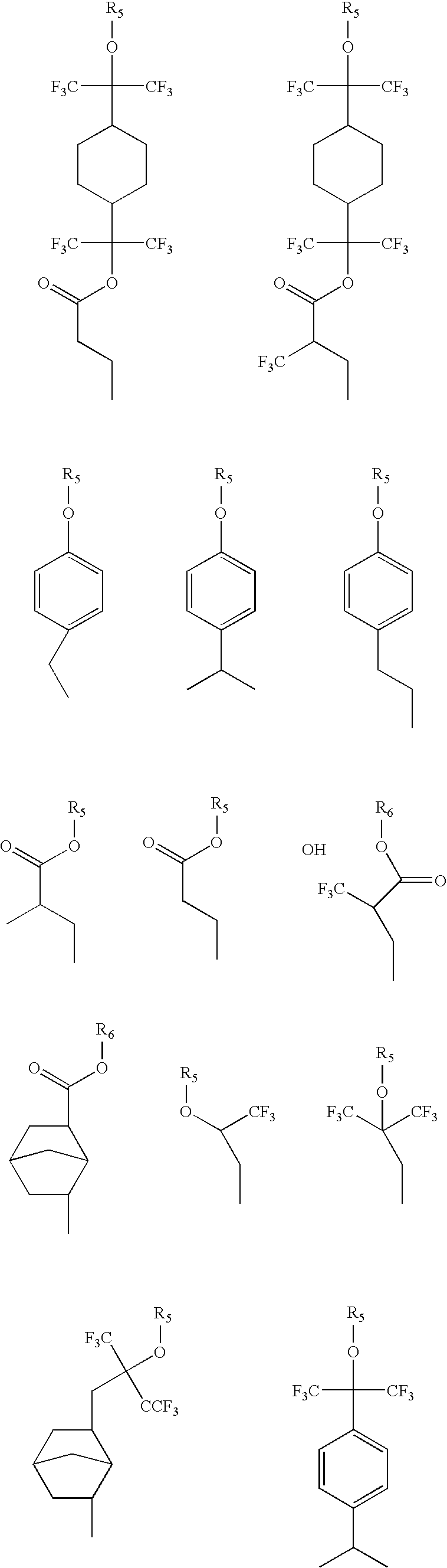
Priority Applications (1)
| Application Number | Priority Date | Filing Date | Title |
|---|---|---|---|
| US11/933,530 US7714079B2 (en) | 2003-01-08 | 2007-11-01 | Patternable low dielectric constant materials and their use in ULSI interconnection |
Applications Claiming Priority (3)
| Application Number | Priority Date | Filing Date | Title |
|---|---|---|---|
| US10/338,945 US7041748B2 (en) | 2003-01-08 | 2003-01-08 | Patternable low dielectric constant materials and their use in ULSI interconnection |
| US11/314,307 US7306853B2 (en) | 2003-01-08 | 2005-12-21 | Patternable low dielectric constant materials and their use in ULSI interconnection |
| US11/933,530 US7714079B2 (en) | 2003-01-08 | 2007-11-01 | Patternable low dielectric constant materials and their use in ULSI interconnection |
Related Parent Applications (1)
| Application Number | Title | Priority Date | Filing Date |
|---|---|---|---|
| US11/314,307 Division US7306853B2 (en) | 2003-01-08 | 2005-12-21 | Patternable low dielectric constant materials and their use in ULSI interconnection |
Publications (2)
| Publication Number | Publication Date |
|---|---|
| US20080063880A1 US20080063880A1 (en) | 2008-03-13 |
| US7714079B2 true US7714079B2 (en) | 2010-05-11 |
Family
ID=32711012
Family Applications (3)
| Application Number | Title | Priority Date | Filing Date |
|---|---|---|---|
| US10/338,945 Expired - Lifetime US7041748B2 (en) | 2003-01-08 | 2003-01-08 | Patternable low dielectric constant materials and their use in ULSI interconnection |
| US11/314,307 Expired - Fee Related US7306853B2 (en) | 2003-01-08 | 2005-12-21 | Patternable low dielectric constant materials and their use in ULSI interconnection |
| US11/933,530 Expired - Fee Related US7714079B2 (en) | 2003-01-08 | 2007-11-01 | Patternable low dielectric constant materials and their use in ULSI interconnection |
Family Applications Before (2)
| Application Number | Title | Priority Date | Filing Date |
|---|---|---|---|
| US10/338,945 Expired - Lifetime US7041748B2 (en) | 2003-01-08 | 2003-01-08 | Patternable low dielectric constant materials and their use in ULSI interconnection |
| US11/314,307 Expired - Fee Related US7306853B2 (en) | 2003-01-08 | 2005-12-21 | Patternable low dielectric constant materials and their use in ULSI interconnection |
Country Status (4)
| Country | Link |
|---|---|
| US (3) | US7041748B2 (en) |
| JP (1) | JP3935874B2 (en) |
| KR (1) | KR100562238B1 (en) |
| TW (1) | TWI320515B (en) |
Cited By (3)
| Publication number | Priority date | Publication date | Assignee | Title |
|---|---|---|---|---|
| US20070254235A1 (en) * | 2006-04-28 | 2007-11-01 | International Business Machines Corporation | Self-topcoating resist for photolithography |
| US8334203B2 (en) | 2010-06-11 | 2012-12-18 | International Business Machines Corporation | Interconnect structure and method of fabricating |
| US9837314B2 (en) * | 2016-02-02 | 2017-12-05 | Tokyo Electron Limited | Self-alignment of metal and via using selective deposition |
Families Citing this family (116)
| Publication number | Priority date | Publication date | Assignee | Title |
|---|---|---|---|---|
| US7261992B2 (en) * | 2000-12-21 | 2007-08-28 | International Business Machines Corporation | Fluorinated silsesquioxane polymers and use thereof in lithographic photoresist compositions |
| TWI288443B (en) | 2002-05-17 | 2007-10-11 | Semiconductor Energy Lab | SiN film, semiconductor device, and the manufacturing method thereof |
| US7507783B2 (en) * | 2003-02-24 | 2009-03-24 | Brewer Science Inc. | Thermally curable middle layer comprising polyhedral oligomeric silsesouioxanes for 193-nm trilayer resist process |
| US7098149B2 (en) * | 2003-03-04 | 2006-08-29 | Air Products And Chemicals, Inc. | Mechanical enhancement of dense and porous organosilicate materials by UV exposure |
| TWI240959B (en) | 2003-03-04 | 2005-10-01 | Air Prod & Chem | Mechanical enhancement of dense and porous organosilicate materials by UV exposure |
| JP4734832B2 (en) * | 2003-05-14 | 2011-07-27 | ナガセケムテックス株式会社 | Encapsulant for optical element |
| US7867331B2 (en) * | 2003-08-04 | 2011-01-11 | Honeywell International Inc. | Coating composition optimization for via fill and photolithography applications and methods of preparation thereof |
| JP5102428B2 (en) * | 2003-11-25 | 2012-12-19 | ローム・アンド・ハース・エレクトロニック・マテリアルズ,エル.エル.シー. | Waveguide composition and waveguide formed therefrom |
| KR100586165B1 (en) * | 2003-12-30 | 2006-06-07 | 동부일렉트로닉스 주식회사 | Floor anti-reflective coating method |
| US7355384B2 (en) * | 2004-04-08 | 2008-04-08 | International Business Machines Corporation | Apparatus, method, and computer program product for monitoring and controlling a microcomputer using a single existing pin |
| US7629272B2 (en) * | 2004-06-07 | 2009-12-08 | Axcelis Technologies, Inc. | Ultraviolet assisted porogen removal and/or curing processes for forming porous low k dielectrics |
| US7563828B2 (en) * | 2004-07-16 | 2009-07-21 | Alcatel-Lucent Usa Inc. | Solid state proton conductor system derived from hybrid composite inorganic-organic multicomponent material |
| JP2006156602A (en) * | 2004-11-26 | 2006-06-15 | Asahi Kasei Corp | Insulation film |
| US7985677B2 (en) * | 2004-11-30 | 2011-07-26 | Semiconductor Energy Laboratory Co., Ltd. | Method of manufacturing semiconductor device |
| US7732349B2 (en) * | 2004-11-30 | 2010-06-08 | Semiconductor Energy Laboratory Co., Ltd. | Manufacturing method of insulating film and semiconductor device |
| US7696625B2 (en) | 2004-11-30 | 2010-04-13 | Semiconductor Energy Laboratory Co., Ltd. | Semiconductor device and method for manufacturing the same |
| US7579224B2 (en) * | 2005-01-21 | 2009-08-25 | Semiconductor Energy Laboratory Co., Ltd. | Method for manufacturing a thin film semiconductor device |
| US7399581B2 (en) * | 2005-02-24 | 2008-07-15 | International Business Machines Corporation | Photoresist topcoat for a photolithographic process |
| US8012673B1 (en) * | 2005-03-01 | 2011-09-06 | Spansion Llc | Processing a copolymer to form a polymer memory cell |
| JP4450214B2 (en) * | 2005-03-11 | 2010-04-14 | セイコーエプソン株式会社 | Organic thin film transistor, electronic device and electronic equipment |
| JP4775561B2 (en) * | 2005-04-01 | 2011-09-21 | 信越化学工業株式会社 | Silsesquioxane-based compound mixture, production method thereof, resist composition using the same, and pattern formation method |
| US7960442B2 (en) * | 2005-04-20 | 2011-06-14 | International Business Machines Corporation | Nanoporous media templated from unsymmetrical amphiphilic porogens |
| US7482389B2 (en) | 2005-04-20 | 2009-01-27 | International Business Machines Corporation | Nanoporous media with lamellar structures |
| US7723438B2 (en) * | 2005-04-28 | 2010-05-25 | International Business Machines Corporation | Surface-decorated polymeric amphiphile porogens for the templation of nanoporous materials |
| US7224050B2 (en) * | 2005-05-25 | 2007-05-29 | Intel Corporation | Plastic materials including dendrimers or hyperbranched polymers for integrated circuit packaging |
| JP4602842B2 (en) * | 2005-06-07 | 2010-12-22 | 東京応化工業株式会社 | Anti-reflection film forming composition and anti-reflection film using the same |
| US7459183B2 (en) * | 2005-07-27 | 2008-12-02 | International Business Machines Corporation | Method of forming low-K interlevel dielectric layers and structures |
| JP4692136B2 (en) * | 2005-08-08 | 2011-06-01 | 東レ株式会社 | Photosensitive paste composition and field emission display member using the same |
| US7449538B2 (en) * | 2005-12-30 | 2008-11-11 | Hynix Semiconductor Inc. | Hard mask composition and method for manufacturing semiconductor device |
| US7468330B2 (en) * | 2006-04-05 | 2008-12-23 | International Business Machines Corporation | Imprint process using polyhedral oligomeric silsesquioxane based imprint materials |
| JP2007293159A (en) * | 2006-04-27 | 2007-11-08 | Asahi Kasei Corp | Photosensitive resin composition and silsesquioxane polymer |
| US7704670B2 (en) | 2006-06-22 | 2010-04-27 | Az Electronic Materials Usa Corp. | High silicon-content thin film thermosets |
| KR101293937B1 (en) * | 2006-06-28 | 2013-08-09 | 다우 코닝 코포레이션 | Silsesquioxane resin systems with base additives bearing electron-attracting functionalities |
| WO2008002970A2 (en) * | 2006-06-28 | 2008-01-03 | Dow Corning Corporation | Silsesquioxane resin systems with base additives bearing electron-attracting functionalities |
| US7927664B2 (en) * | 2006-08-28 | 2011-04-19 | International Business Machines Corporation | Method of step-and-flash imprint lithography |
| JP4509080B2 (en) | 2006-09-28 | 2010-07-21 | 信越化学工業株式会社 | Silsesquioxane compound mixture, hydrolyzable silane compound, production method thereof, resist composition using the same, pattern formation method, and substrate processing method |
| US8053375B1 (en) * | 2006-11-03 | 2011-11-08 | Advanced Technology Materials, Inc. | Super-dry reagent compositions for formation of ultra low k films |
| US8026040B2 (en) * | 2007-02-20 | 2011-09-27 | Az Electronic Materials Usa Corp. | Silicone coating composition |
| US7736837B2 (en) * | 2007-02-20 | 2010-06-15 | Az Electronic Materials Usa Corp. | Antireflective coating composition based on silicon polymer |
| KR20090114476A (en) * | 2007-02-26 | 2009-11-03 | 에이제트 일렉트로닉 머트리얼즈 유에스에이 코프. | Process for preparing siloxane polymer |
| CN101622296B (en) * | 2007-02-27 | 2013-10-16 | Az电子材料美国公司 | Silicon-based antifrelective coating compositions |
| JP4963254B2 (en) * | 2007-03-30 | 2012-06-27 | 東京応化工業株式会社 | Film-forming composition for nanoimprint, structure manufacturing method and structure |
| US8084765B2 (en) * | 2007-05-07 | 2011-12-27 | Xerox Corporation | Electronic device having a dielectric layer |
| US7867689B2 (en) * | 2007-05-18 | 2011-01-11 | International Business Machines Corporation | Method of use for photopatternable dielectric materials for BEOL applications |
| US8470516B2 (en) * | 2007-05-18 | 2013-06-25 | International Business Machines Corporation | Method of forming a relief pattern by e-beam lithography using chemical amplification, and derived articles |
| US8084862B2 (en) * | 2007-09-20 | 2011-12-27 | International Business Machines Corporation | Interconnect structures with patternable low-k dielectrics and method of fabricating same |
| US7709370B2 (en) * | 2007-09-20 | 2010-05-04 | International Business Machines Corporation | Spin-on antireflective coating for integration of patternable dielectric materials and interconnect structures |
| US8618663B2 (en) | 2007-09-20 | 2013-12-31 | International Business Machines Corporation | Patternable dielectric film structure with improved lithography and method of fabricating same |
| KR100936998B1 (en) * | 2007-10-19 | 2010-01-15 | 에스화인켐 주식회사 | Photosensitive polysilsesquioxane resin composition and pattern formation method of a thin film using the same |
| KR101800015B1 (en) * | 2007-12-10 | 2017-11-21 | 카네카 코포레이션 | Alkali-developable curable composition, insulating thin film using the same, and thin film transistor |
| US20090174036A1 (en) * | 2008-01-04 | 2009-07-09 | International Business Machines Corporation | Plasma curing of patterning materials for aggressively scaled features |
| US8476758B2 (en) * | 2008-01-09 | 2013-07-02 | International Business Machines Corporation | Airgap-containing interconnect structure with patternable low-k material and method of fabricating |
| US7977256B2 (en) * | 2008-03-06 | 2011-07-12 | Tokyo Electron Limited | Method for removing a pore-generating material from an uncured low-k dielectric film |
| US8029971B2 (en) * | 2008-03-13 | 2011-10-04 | International Business Machines Corporation | Photopatternable dielectric materials for BEOL applications and methods for use |
| CN104497272B (en) | 2008-10-02 | 2017-06-23 | 株式会社钟化 | Photocurable composition and solidfied material |
| EP2189846B1 (en) * | 2008-11-19 | 2015-04-22 | Rohm and Haas Electronic Materials LLC | Process for photolithography applying a photoresist composition comprising a block copolymer |
| US8227336B2 (en) * | 2009-01-20 | 2012-07-24 | International Business Machines Corporation | Structure with self aligned resist layer on an interconnect surface and method of making same |
| US8168691B2 (en) * | 2009-02-09 | 2012-05-01 | International Business Machines Corporation | Vinyl ether resist formulations for imprint lithography and processes of use |
| KR101715343B1 (en) * | 2009-03-11 | 2017-03-14 | 주식회사 동진쎄미켐 | Method for forming fine pattern in semiconductor device |
| US8728710B2 (en) * | 2009-03-31 | 2014-05-20 | Sam Xunyun Sun | Photo-imageable hardmask with dual tones for microphotolithography |
| US8911932B2 (en) * | 2009-04-13 | 2014-12-16 | Sam Xunyun Sun | Photo-imageable hardmask with positive tone for microphotolithography |
| US8298937B2 (en) * | 2009-06-12 | 2012-10-30 | International Business Machines Corporation | Interconnect structure fabricated without dry plasma etch processing |
| US8519540B2 (en) | 2009-06-16 | 2013-08-27 | International Business Machines Corporation | Self-aligned dual damascene BEOL structures with patternable low- K material and methods of forming same |
| US8659115B2 (en) * | 2009-06-17 | 2014-02-25 | International Business Machines Corporation | Airgap-containing interconnect structure with improved patternable low-K material and method of fabricating |
| US8168109B2 (en) * | 2009-08-21 | 2012-05-01 | International Business Machines Corporation | Stabilizers for vinyl ether resist formulations for imprint lithography |
| US8163658B2 (en) * | 2009-08-24 | 2012-04-24 | International Business Machines Corporation | Multiple patterning using improved patternable low-k dielectric materials |
| JP5381508B2 (en) * | 2009-08-27 | 2014-01-08 | Jsr株式会社 | Negative radiation sensitive composition, cured pattern forming method, and cured pattern |
| KR101666097B1 (en) * | 2009-08-27 | 2016-10-13 | 삼성전자 주식회사 | Polyurethane foam composition and polyurethane foam prepared using same |
| US8431670B2 (en) * | 2009-08-31 | 2013-04-30 | International Business Machines Corporation | Photo-patternable dielectric materials and formulations and methods of use |
| US8202783B2 (en) * | 2009-09-29 | 2012-06-19 | International Business Machines Corporation | Patternable low-k dielectric interconnect structure with a graded cap layer and method of fabrication |
| US8377631B2 (en) * | 2009-10-06 | 2013-02-19 | International Business Machines Corporation | Planarization over topography with molecular glass materials |
| US8389663B2 (en) * | 2009-10-08 | 2013-03-05 | International Business Machines Corporation | Photo-patternable dielectric materials curable to porous dielectric materials, formulations, precursors and methods of use thereof |
| US8637395B2 (en) * | 2009-11-16 | 2014-01-28 | International Business Machines Corporation | Methods for photo-patternable low-k (PPLK) integration with curing after pattern transfer |
| US8367540B2 (en) * | 2009-11-19 | 2013-02-05 | International Business Machines Corporation | Interconnect structure including a modified photoresist as a permanent interconnect dielectric and method of fabricating same |
| US8642252B2 (en) | 2010-03-10 | 2014-02-04 | International Business Machines Corporation | Methods for fabrication of an air gap-containing interconnect structure |
| US8896120B2 (en) | 2010-04-27 | 2014-11-25 | International Business Machines Corporation | Structures and methods for air gap integration |
| US8241992B2 (en) | 2010-05-10 | 2012-08-14 | International Business Machines Corporation | Method for air gap interconnect integration using photo-patternable low k material |
| US8373271B2 (en) | 2010-05-27 | 2013-02-12 | International Business Machines Corporation | Interconnect structure with an oxygen-doped SiC antireflective coating and method of fabrication |
| US8853856B2 (en) | 2010-06-22 | 2014-10-07 | International Business Machines Corporation | Methodology for evaluation of electrical characteristics of carbon nanotubes |
| US8475667B2 (en) | 2010-06-22 | 2013-07-02 | International Business Machines Corporation | Method of patterning photosensitive material on a substrate containing a latent acid generator |
| US8449781B2 (en) | 2010-06-22 | 2013-05-28 | International Business Machines Corporation | Selective etch back process for carbon nanotubes intergration |
| CN101880374B (en) * | 2010-07-09 | 2011-11-30 | 中南民族大学 | Silicon framework hyperbranched epoxy resin and preparation method thereof |
| US8354339B2 (en) | 2010-07-20 | 2013-01-15 | International Business Machines Corporation | Methods to form self-aligned permanent on-chip interconnect structures |
| US8232198B2 (en) | 2010-08-05 | 2012-07-31 | International Business Machines Corporation | Self-aligned permanent on-chip interconnect structure formed by pitch splitting |
| JP2012094726A (en) * | 2010-10-28 | 2012-05-17 | Fujitsu Ltd | Field-effect transistor and method of manufacturing the same |
| US8623447B2 (en) * | 2010-12-01 | 2014-01-07 | Xerox Corporation | Method for coating dielectric composition for fabricating thin-film transistors |
| US8441006B2 (en) * | 2010-12-23 | 2013-05-14 | Intel Corporation | Cyclic carbosilane dielectric films |
| US8617941B2 (en) | 2011-01-16 | 2013-12-31 | International Business Machines Corporation | High-speed graphene transistor and method of fabrication by patternable hard mask materials |
| EP2691810A1 (en) * | 2011-03-29 | 2014-02-05 | Dow Corning Corporation | Photo-patternable and developable silesquioxane resins for use in device fabrication |
| US9054160B2 (en) | 2011-04-15 | 2015-06-09 | International Business Machines Corporation | Interconnect structure and method for fabricating on-chip interconnect structures by image reversal |
| US8890318B2 (en) | 2011-04-15 | 2014-11-18 | International Business Machines Corporation | Middle of line structures |
| US8900988B2 (en) | 2011-04-15 | 2014-12-02 | International Business Machines Corporation | Method for forming self-aligned airgap interconnect structures |
| US8822137B2 (en) * | 2011-08-03 | 2014-09-02 | International Business Machines Corporation | Self-aligned fine pitch permanent on-chip interconnect structures and method of fabrication |
| US8614047B2 (en) * | 2011-08-26 | 2013-12-24 | International Business Machines Corporation | Photodecomposable bases and photoresist compositions |
| US20130062732A1 (en) | 2011-09-08 | 2013-03-14 | International Business Machines Corporation | Interconnect structures with functional components and methods for fabrication |
| JP2013149861A (en) * | 2012-01-20 | 2013-08-01 | Sumitomo Chemical Co Ltd | Organic thin-film transistor insulating layer material |
| US8871425B2 (en) * | 2012-02-09 | 2014-10-28 | Az Electronic Materials (Luxembourg) S.A.R.L. | Low dielectric photoimageable compositions and electronic devices made therefrom |
| US9087753B2 (en) | 2012-05-10 | 2015-07-21 | International Business Machines Corporation | Printed transistor and fabrication method |
| CN110209014A (en) * | 2012-07-04 | 2019-09-06 | 株式会社钟化 | Positive light sensitivity composition, thin film transistor (TFT) and compound |
| JP6086739B2 (en) * | 2013-01-21 | 2017-03-01 | 東京応化工業株式会社 | Insulating film forming composition, insulating film manufacturing method, and insulating film |
| CN103214510B (en) * | 2013-04-10 | 2015-06-24 | 吉林大学 | Octohydroxy cage-like silsesquioxane monomer and preparation method thereof |
| JP6429031B2 (en) | 2013-10-30 | 2018-11-28 | 日産化学株式会社 | Imprint material containing silsesquioxane compound and modified silicone compound |
| JP6323225B2 (en) * | 2013-11-01 | 2018-05-16 | セントラル硝子株式会社 | Positive photosensitive resin composition, film production method using the same, and electronic component |
| CN103579102A (en) * | 2013-11-07 | 2014-02-12 | 复旦大学 | Method for preparing low dielectric constant film with excellent mechanical property |
| CN103613611A (en) * | 2013-12-06 | 2014-03-05 | 吉林大学 | Polyhedral oligomeric silsesquioxane with 16-hydroxy and preparation method thereof |
| JP6260579B2 (en) * | 2015-05-01 | 2018-01-17 | 信越化学工業株式会社 | Fluoropolyether group-containing polymer-modified silane, surface treatment agent and article |
| US10269623B2 (en) | 2015-06-22 | 2019-04-23 | Intel Corporation | Image tone-reversal with a dielectric using bottom-up cross-linking for back end of line (BEOL) interconnects |
| JPWO2017056888A1 (en) * | 2015-09-30 | 2018-08-09 | 富士フイルム株式会社 | Pattern forming method and actinic ray-sensitive or radiation-sensitive resin composition |
| CN105254661A (en) * | 2015-10-23 | 2016-01-20 | 航天材料及工艺研究所 | Cage-shaped oligomerization polyhedral silsesquioxane with eight phenolic hydroxyl groups and preparation method thereof |
| CN109415513B (en) * | 2016-06-16 | 2022-02-25 | 美国陶氏有机硅公司 | Silicon-rich silsesquioxane resins |
| KR102242545B1 (en) * | 2017-09-27 | 2021-04-19 | 주식회사 엘지화학 | Antibacterial polymer coating composition and antibacterial polymer film |
| US10573687B2 (en) | 2017-10-31 | 2020-02-25 | International Business Machines Corporation | Magnetic random access memory with permanent photo-patternable low-K dielectric |
| US10950549B2 (en) | 2018-11-16 | 2021-03-16 | International Business Machines Corporation | ILD gap fill for memory device stack array |
| WO2020175338A1 (en) | 2019-02-27 | 2020-09-03 | 富士フイルム株式会社 | Polyorganosilsesquioxane and hard coat layer-forming composition |
| CN114063389A (en) * | 2020-07-31 | 2022-02-18 | 华为技术有限公司 | Patterned material and patterned thin film |
| CN116547290A (en) * | 2020-11-03 | 2023-08-04 | Oti照明公司 | Silicon-containing compounds for forming patterned coatings and devices comprising the same |
Citations (31)
| Publication number | Priority date | Publication date | Assignee | Title |
|---|---|---|---|---|
| JPS6080851A (en) | 1983-10-11 | 1985-05-08 | Nippon Telegr & Teleph Corp <Ntt> | Pattern forming material and formation of pattern |
| US5290899A (en) | 1988-09-22 | 1994-03-01 | Tosoh Corporation | Photosensitive material having a silicon-containing polymer |
| US5338818A (en) | 1992-09-10 | 1994-08-16 | International Business Machines Corporation | Silicon containing positive resist for DUV lithography |
| US5385804A (en) | 1992-08-20 | 1995-01-31 | International Business Machines Corporation | Silicon containing negative resist for DUV, I-line or E-beam lithography comprising an aromatic azide side group in the polysilsesquioxane polymer |
| US5422223A (en) | 1992-04-30 | 1995-06-06 | International Business Machines Corporation | Silicon-containing positive resist and use in multilayer metal structures |
| US5789460A (en) | 1995-02-02 | 1998-08-04 | Dow Corning Asia, Ltd. | Radiation curable compositions |
| US5820944A (en) | 1996-04-01 | 1998-10-13 | Dow Corning Asia, Ltd. | Ultraviolet-curable composition and method for forming cured-product patterns therefrom |
| US5861235A (en) | 1996-06-26 | 1999-01-19 | Dow Corning Asia, Ltd. | Ultraviolet-curable composition and method for patterning the cured product therefrom |
| US6051625A (en) | 1996-06-27 | 2000-04-18 | Dow Corning Asia, Ltd. | Ultraviolet-curable polysiloxane composition and method for the formation of cured patterns therefrom |
| US6087064A (en) | 1998-09-03 | 2000-07-11 | International Business Machines Corporation | Silsesquioxane polymers, method of synthesis, photoresist composition, and multilayer lithographic method |
| US6096483A (en) | 1996-03-29 | 2000-08-01 | Dow Corning Asia, Ltd. | Radiation-curable composition and method for manufacturing cured-product patterns therefrom |
| US6107357A (en) | 1999-11-16 | 2000-08-22 | International Business Machines Corporatrion | Dielectric compositions and method for their manufacture |
| JP2000281790A (en) | 1999-03-30 | 2000-10-10 | Nippon Steel Chem Co Ltd | Silicone resin and photosensitive resin composition containing the same |
| US6187505B1 (en) | 1999-02-02 | 2001-02-13 | International Business Machines Corporation | Radiation sensitive silicon-containing resists |
| US6191183B1 (en) | 1997-02-24 | 2001-02-20 | Dow Corning Toray Silicone Co., Ltd. | Method for the formation of silica thin films |
| US6251486B1 (en) | 1997-09-09 | 2001-06-26 | Agere Systems Guardian Corp. | Method for coating an article with a ladder siloxane polymer and coated article |
| US6271273B1 (en) | 2000-07-14 | 2001-08-07 | Shipley Company, L.L.C. | Porous materials |
| US6342562B1 (en) | 1999-04-23 | 2002-01-29 | Fujitsu Limited | Silicon-containing polymer, process for its production, resist composition employing it, pattern-forming method and electronic device fabrication method |
| US6420088B1 (en) | 2000-06-23 | 2002-07-16 | International Business Machines Corporation | Antireflective silicon-containing compositions as hardmask layer |
| US6420441B1 (en) | 1999-10-01 | 2002-07-16 | Shipley Company, L.L.C. | Porous materials |
| US6420084B1 (en) | 2000-06-23 | 2002-07-16 | International Business Machines Corporation | Mask-making using resist having SIO bond-containing polymer |
| US6472076B1 (en) | 1999-10-18 | 2002-10-29 | Honeywell International Inc. | Deposition of organosilsesquioxane films |
| US6531260B2 (en) | 2000-04-07 | 2003-03-11 | Jsr Corporation | Polysiloxane, method of manufacturing same, silicon-containing alicyclic compound, and radiation-sensitive resin composition |
| US20030073040A1 (en) | 2001-08-24 | 2003-04-17 | Haruo Iwasawa | Pattern forming method and bilayer film |
| US20030099899A1 (en) | 2001-05-08 | 2003-05-29 | Gronbeck Dana A. | Photoimageable composition |
| US6576345B1 (en) | 2000-11-30 | 2003-06-10 | Novellus Systems Inc | Dielectric films with low dielectric constants |
| US6653045B2 (en) | 2001-02-16 | 2003-11-25 | International Business Machines Corporation | Radiation sensitive silicon-containing negative resists and use thereof |
| US6762501B1 (en) | 2003-04-14 | 2004-07-13 | Texas Instruments Incorporated | Low stress integrated circuit copper interconnect structures |
| US20040138355A1 (en) * | 2001-01-24 | 2004-07-15 | Hideo Saito | Polyphentlene ether resin composition containing silicon compounds |
| US6774031B2 (en) * | 2002-12-17 | 2004-08-10 | Texas Instruments Incorporated | Method of forming dual-damascene structure |
| US6873026B1 (en) | 2002-03-04 | 2005-03-29 | Novellus Systems, Inc. | Inhomogeneous materials having physical properties decoupled from desired functions |
Family Cites Families (1)
| Publication number | Priority date | Publication date | Assignee | Title |
|---|---|---|---|---|
| JP2000501070A (en) * | 1995-09-28 | 2000-02-02 | メルク シヤープ エンド ドーム リミテツド | Substituted indolylpropylpiperazine derivatives as 5-HT 1Dα agonists |
-
2003
- 2003-01-08 US US10/338,945 patent/US7041748B2/en not_active Expired - Lifetime
- 2003-12-08 KR KR1020030088568A patent/KR100562238B1/en not_active Expired - Fee Related
- 2003-12-18 JP JP2003421691A patent/JP3935874B2/en not_active Expired - Lifetime
-
2004
- 2004-01-05 TW TW93100144A patent/TWI320515B/en not_active IP Right Cessation
-
2005
- 2005-12-21 US US11/314,307 patent/US7306853B2/en not_active Expired - Fee Related
-
2007
- 2007-11-01 US US11/933,530 patent/US7714079B2/en not_active Expired - Fee Related
Patent Citations (35)
| Publication number | Priority date | Publication date | Assignee | Title |
|---|---|---|---|---|
| JPS6080851A (en) | 1983-10-11 | 1985-05-08 | Nippon Telegr & Teleph Corp <Ntt> | Pattern forming material and formation of pattern |
| US5290899A (en) | 1988-09-22 | 1994-03-01 | Tosoh Corporation | Photosensitive material having a silicon-containing polymer |
| US5422223A (en) | 1992-04-30 | 1995-06-06 | International Business Machines Corporation | Silicon-containing positive resist and use in multilayer metal structures |
| US5385804A (en) | 1992-08-20 | 1995-01-31 | International Business Machines Corporation | Silicon containing negative resist for DUV, I-line or E-beam lithography comprising an aromatic azide side group in the polysilsesquioxane polymer |
| US5338818A (en) | 1992-09-10 | 1994-08-16 | International Business Machines Corporation | Silicon containing positive resist for DUV lithography |
| US5891529A (en) | 1995-02-02 | 1999-04-06 | Dow Corning Asia, Ltd. | Radiation curable sompositions |
| US5789460A (en) | 1995-02-02 | 1998-08-04 | Dow Corning Asia, Ltd. | Radiation curable compositions |
| US6096483A (en) | 1996-03-29 | 2000-08-01 | Dow Corning Asia, Ltd. | Radiation-curable composition and method for manufacturing cured-product patterns therefrom |
| US5820944A (en) | 1996-04-01 | 1998-10-13 | Dow Corning Asia, Ltd. | Ultraviolet-curable composition and method for forming cured-product patterns therefrom |
| US5861235A (en) | 1996-06-26 | 1999-01-19 | Dow Corning Asia, Ltd. | Ultraviolet-curable composition and method for patterning the cured product therefrom |
| US6051625A (en) | 1996-06-27 | 2000-04-18 | Dow Corning Asia, Ltd. | Ultraviolet-curable polysiloxane composition and method for the formation of cured patterns therefrom |
| US6258506B1 (en) | 1996-06-27 | 2001-07-10 | Dow Corning Asia, Ltd. | Ultraviolet-curable polysiloxane composition and method for the formation of cured patterns therefrom |
| US6191183B1 (en) | 1997-02-24 | 2001-02-20 | Dow Corning Toray Silicone Co., Ltd. | Method for the formation of silica thin films |
| US6251486B1 (en) | 1997-09-09 | 2001-06-26 | Agere Systems Guardian Corp. | Method for coating an article with a ladder siloxane polymer and coated article |
| US6087064A (en) | 1998-09-03 | 2000-07-11 | International Business Machines Corporation | Silsesquioxane polymers, method of synthesis, photoresist composition, and multilayer lithographic method |
| US6340734B1 (en) | 1998-09-03 | 2002-01-22 | International Business Machines Corporation | Silsesquioxane polymers, method of synthesis, photoresist composition, and multilayer lithographic method |
| US6187505B1 (en) | 1999-02-02 | 2001-02-13 | International Business Machines Corporation | Radiation sensitive silicon-containing resists |
| JP2000281790A (en) | 1999-03-30 | 2000-10-10 | Nippon Steel Chem Co Ltd | Silicone resin and photosensitive resin composition containing the same |
| US6767983B1 (en) | 1999-03-30 | 2004-07-27 | Nippon Steel Chemical Co., Ltd. | Silicone resin and photosensitive resin composition containing the same |
| US6342562B1 (en) | 1999-04-23 | 2002-01-29 | Fujitsu Limited | Silicon-containing polymer, process for its production, resist composition employing it, pattern-forming method and electronic device fabrication method |
| US6420441B1 (en) | 1999-10-01 | 2002-07-16 | Shipley Company, L.L.C. | Porous materials |
| US6472076B1 (en) | 1999-10-18 | 2002-10-29 | Honeywell International Inc. | Deposition of organosilsesquioxane films |
| US6107357A (en) | 1999-11-16 | 2000-08-22 | International Business Machines Corporatrion | Dielectric compositions and method for their manufacture |
| US6531260B2 (en) | 2000-04-07 | 2003-03-11 | Jsr Corporation | Polysiloxane, method of manufacturing same, silicon-containing alicyclic compound, and radiation-sensitive resin composition |
| US6420088B1 (en) | 2000-06-23 | 2002-07-16 | International Business Machines Corporation | Antireflective silicon-containing compositions as hardmask layer |
| US6420084B1 (en) | 2000-06-23 | 2002-07-16 | International Business Machines Corporation | Mask-making using resist having SIO bond-containing polymer |
| US6271273B1 (en) | 2000-07-14 | 2001-08-07 | Shipley Company, L.L.C. | Porous materials |
| US6576345B1 (en) | 2000-11-30 | 2003-06-10 | Novellus Systems Inc | Dielectric films with low dielectric constants |
| US20040138355A1 (en) * | 2001-01-24 | 2004-07-15 | Hideo Saito | Polyphentlene ether resin composition containing silicon compounds |
| US6653045B2 (en) | 2001-02-16 | 2003-11-25 | International Business Machines Corporation | Radiation sensitive silicon-containing negative resists and use thereof |
| US20030099899A1 (en) | 2001-05-08 | 2003-05-29 | Gronbeck Dana A. | Photoimageable composition |
| US20030073040A1 (en) | 2001-08-24 | 2003-04-17 | Haruo Iwasawa | Pattern forming method and bilayer film |
| US6873026B1 (en) | 2002-03-04 | 2005-03-29 | Novellus Systems, Inc. | Inhomogeneous materials having physical properties decoupled from desired functions |
| US6774031B2 (en) * | 2002-12-17 | 2004-08-10 | Texas Instruments Incorporated | Method of forming dual-damascene structure |
| US6762501B1 (en) | 2003-04-14 | 2004-07-13 | Texas Instruments Incorporated | Low stress integrated circuit copper interconnect structures |
Non-Patent Citations (2)
| Title |
|---|
| "Silsesquioxanes as models for silica surfaces", J. Amer. Chem. Soc., 1989, 111 (5), 1741-1748, to Frank J. Feher, David A. Newman and John F. Walzer. * |
| Harkness, et al., "Demonstration of a Directly Photopatternable Spin-On-Glass Based on Hydrogen Silsesquioxane and Photobase Generators", Macromolecules, American Chemical Society, 1998, 31, pp. 4798-4805. |
Cited By (5)
| Publication number | Priority date | Publication date | Assignee | Title |
|---|---|---|---|---|
| US20070254235A1 (en) * | 2006-04-28 | 2007-11-01 | International Business Machines Corporation | Self-topcoating resist for photolithography |
| US8945808B2 (en) * | 2006-04-28 | 2015-02-03 | International Business Machines Corporation | Self-topcoating resist for photolithography |
| US8334203B2 (en) | 2010-06-11 | 2012-12-18 | International Business Machines Corporation | Interconnect structure and method of fabricating |
| US8916978B2 (en) | 2010-06-11 | 2014-12-23 | International Business Machines Corporation | Interconnect structure and method of fabricating |
| US9837314B2 (en) * | 2016-02-02 | 2017-12-05 | Tokyo Electron Limited | Self-alignment of metal and via using selective deposition |
Also Published As
| Publication number | Publication date |
|---|---|
| US20040137241A1 (en) | 2004-07-15 |
| US20080063880A1 (en) | 2008-03-13 |
| US20060105181A1 (en) | 2006-05-18 |
| JP3935874B2 (en) | 2007-06-27 |
| KR20040063769A (en) | 2004-07-14 |
| US7041748B2 (en) | 2006-05-09 |
| JP2004212983A (en) | 2004-07-29 |
| TWI320515B (en) | 2010-02-11 |
| KR100562238B1 (en) | 2006-03-22 |
| US7306853B2 (en) | 2007-12-11 |
| TW200508803A (en) | 2005-03-01 |
Similar Documents
| Publication | Publication Date | Title |
|---|---|---|
| US7714079B2 (en) | Patternable low dielectric constant materials and their use in ULSI interconnection | |
| US7709370B2 (en) | Spin-on antireflective coating for integration of patternable dielectric materials and interconnect structures | |
| US7172849B2 (en) | Antireflective hardmask and uses thereof | |
| US7666794B2 (en) | Multiple patterning using patternable low-k dielectric materials | |
| JP5285814B2 (en) | Patternable low-k dielectric wiring structure with stepped cap layer, air gap inclusion wiring structure, and fabrication method | |
| CN100426140C (en) | Silicon-containing compositions for spin-on arc/hardmask materials | |
| US7867689B2 (en) | Method of use for photopatternable dielectric materials for BEOL applications | |
| US7919225B2 (en) | Photopatternable dielectric materials for BEOL applications and methods for use | |
| US8659115B2 (en) | Airgap-containing interconnect structure with improved patternable low-K material and method of fabricating | |
| US8389663B2 (en) | Photo-patternable dielectric materials curable to porous dielectric materials, formulations, precursors and methods of use thereof | |
| US8487411B2 (en) | Multiple patterning using improved patternable low-κ dielectric materials | |
| US20140131880A1 (en) | Methods for fabrication of an air gap-containing interconnect structure | |
| US8232198B2 (en) | Self-aligned permanent on-chip interconnect structure formed by pitch splitting | |
| US8431670B2 (en) | Photo-patternable dielectric materials and formulations and methods of use | |
| US20110115090A1 (en) | Interconnect structure including a modified photoresist as a permanent interconnect dielectric and method of fabricating same |
Legal Events
| Date | Code | Title | Description |
|---|---|---|---|
| FEPP | Fee payment procedure |
Free format text: PAYOR NUMBER ASSIGNED (ORIGINAL EVENT CODE: ASPN); ENTITY STATUS OF PATENT OWNER: LARGE ENTITY |
|
| STCF | Information on status: patent grant |
Free format text: PATENTED CASE |
|
| REMI | Maintenance fee reminder mailed | ||
| FPAY | Fee payment |
Year of fee payment: 4 |
|
| SULP | Surcharge for late payment | ||
| AS | Assignment |
Owner name: GLOBALFOUNDRIES U.S. 2 LLC, NEW YORK Free format text: ASSIGNMENT OF ASSIGNORS INTEREST;ASSIGNOR:INTERNATIONAL BUSINESS MACHINES CORPORATION;REEL/FRAME:036550/0001 Effective date: 20150629 |
|
| AS | Assignment |
Owner name: GLOBALFOUNDRIES INC., CAYMAN ISLANDS Free format text: ASSIGNMENT OF ASSIGNORS INTEREST;ASSIGNORS:GLOBALFOUNDRIES U.S. 2 LLC;GLOBALFOUNDRIES U.S. INC.;REEL/FRAME:036779/0001 Effective date: 20150910 |
|
| AS | Assignment |
Owner name: AURIGA INNOVATIONS, INC., CANADA Free format text: ASSIGNMENT OF ASSIGNORS INTEREST;ASSIGNOR:GLOBALFOUNDRIES INC.;REEL/FRAME:041741/0358 Effective date: 20161207 |
|
| MAFP | Maintenance fee payment |
Free format text: PAYMENT OF MAINTENANCE FEE, 8TH YEAR, LARGE ENTITY (ORIGINAL EVENT CODE: M1552) Year of fee payment: 8 |
|
| FEPP | Fee payment procedure |
Free format text: MAINTENANCE FEE REMINDER MAILED (ORIGINAL EVENT CODE: REM.); ENTITY STATUS OF PATENT OWNER: LARGE ENTITY |
|
| LAPS | Lapse for failure to pay maintenance fees |
Free format text: PATENT EXPIRED FOR FAILURE TO PAY MAINTENANCE FEES (ORIGINAL EVENT CODE: EXP.); ENTITY STATUS OF PATENT OWNER: LARGE ENTITY |
|
| STCH | Information on status: patent discontinuation |
Free format text: PATENT EXPIRED DUE TO NONPAYMENT OF MAINTENANCE FEES UNDER 37 CFR 1.362 |
|
| FP | Lapsed due to failure to pay maintenance fee |
Effective date: 20220511 |