US7710174B2 - Digital pulse-width modulator based on non-symmetric self-oscillating circuit - Google Patents
Digital pulse-width modulator based on non-symmetric self-oscillating circuit Download PDFInfo
- Publication number
- US7710174B2 US7710174B2 US12/034,593 US3459308A US7710174B2 US 7710174 B2 US7710174 B2 US 7710174B2 US 3459308 A US3459308 A US 3459308A US 7710174 B2 US7710174 B2 US 7710174B2
- Authority
- US
- United States
- Prior art keywords
- dpwm
- delay
- delay cells
- multiplexer
- output
- Prior art date
- Legal status (The legal status is an assumption and is not a legal conclusion. Google has not performed a legal analysis and makes no representation as to the accuracy of the status listed.)
- Active, expires
Links
- XUIMIQQOPSSXEZ-UHFFFAOYSA-N Silicon Chemical compound [Si] XUIMIQQOPSSXEZ-UHFFFAOYSA-N 0.000 abstract description 7
- 229910052710 silicon Inorganic materials 0.000 abstract description 7
- 239000010703 silicon Substances 0.000 abstract description 7
- 230000010354 integration Effects 0.000 abstract description 3
- 238000010586 diagram Methods 0.000 description 7
- 230000001934 delay Effects 0.000 description 5
- 238000005516 engineering process Methods 0.000 description 4
- 238000000034 method Methods 0.000 description 3
- 230000001902 propagating effect Effects 0.000 description 3
- 230000000630 rising effect Effects 0.000 description 3
- 230000003121 nonmonotonic effect Effects 0.000 description 2
- 230000000644 propagated effect Effects 0.000 description 2
- 239000013078 crystal Substances 0.000 description 1
- 238000012938 design process Methods 0.000 description 1
- 230000000694 effects Effects 0.000 description 1
- 238000012986 modification Methods 0.000 description 1
- 230000004048 modification Effects 0.000 description 1
- 230000010355 oscillation Effects 0.000 description 1
- 229920001690 polydopamine Polymers 0.000 description 1
- 238000013139 quantization Methods 0.000 description 1
- 230000001105 regulatory effect Effects 0.000 description 1
- 238000004088 simulation Methods 0.000 description 1
- 230000007704 transition Effects 0.000 description 1
Images


Classifications
-
- H—ELECTRICITY
- H03—ELECTRONIC CIRCUITRY
- H03K—PULSE TECHNIQUE
- H03K7/00—Modulating pulses with a continuously-variable modulating signal
- H03K7/08—Duration or width modulation ; Duty cycle modulation
-
- H—ELECTRICITY
- H02—GENERATION; CONVERSION OR DISTRIBUTION OF ELECTRIC POWER
- H02M—APPARATUS FOR CONVERSION BETWEEN AC AND AC, BETWEEN AC AND DC, OR BETWEEN DC AND DC, AND FOR USE WITH MAINS OR SIMILAR POWER SUPPLY SYSTEMS; CONVERSION OF DC OR AC INPUT POWER INTO SURGE OUTPUT POWER; CONTROL OR REGULATION THEREOF
- H02M3/00—Conversion of dc power input into dc power output
- H02M3/02—Conversion of dc power input into dc power output without intermediate conversion into ac
- H02M3/04—Conversion of dc power input into dc power output without intermediate conversion into ac by static converters
- H02M3/10—Conversion of dc power input into dc power output without intermediate conversion into ac by static converters using discharge tubes with control electrode or semiconductor devices with control electrode
- H02M3/145—Conversion of dc power input into dc power output without intermediate conversion into ac by static converters using discharge tubes with control electrode or semiconductor devices with control electrode using devices of a triode or transistor type requiring continuous application of a control signal
- H02M3/155—Conversion of dc power input into dc power output without intermediate conversion into ac by static converters using discharge tubes with control electrode or semiconductor devices with control electrode using devices of a triode or transistor type requiring continuous application of a control signal using semiconductor devices only
- H02M3/156—Conversion of dc power input into dc power output without intermediate conversion into ac by static converters using discharge tubes with control electrode or semiconductor devices with control electrode using devices of a triode or transistor type requiring continuous application of a control signal using semiconductor devices only with automatic control of output voltage or current, e.g. switching regulators
Definitions
- CMOS complementary metal-oxide-semiconductor
- PWM pulse-width modulator
- the analog controllers require relatively long design process and need to be almost completely redesigned each time implementation technology changes. As such, they are not suitable for monolithic integration with fast changing digital hardware, on which the majority of portable devices are based.
- CMOS processes not all functional blocks of analog controllers can be implemented due to very limited supply voltages.
- Digital control of low-power SMPS allows easier system integration and, supported by automated design tools, fast transition of designs from one implementation technology to another. Furthermore, the digital control can simplify realization of advanced power management techniques.
- FIG. 1 is a diagram of a digitally controlled switching converter using a DPWM.
- FIG. 2 is a diagram of a DPWM of one embodiment.
- FIG. 3 is a diagram of a digitally programmable-current starved delay cell of one embodiment.
- FIG. 4 is a diagram of a frequency regulator block of one embodiment.
- FIG. 5 is a diagram of an all digital delay cell of one embodiment.
- FIG. 6 is a diagram that shows a portion of a digital controller layout belonging to the DPWM of FIG. 2 .
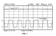
- FIG. 7 is a diagram that shows the operation of an exemplary DPWM.
- the system can regulate the output voltage and operates as follows:
- the output voltage of a power stage which can be any switching power converter, is sampled and compared to a desired reference V ref [n].
- a digital error signal e[n] proportional to the difference between the output and the desired value is formed, if the output voltage is higher than the reference the error is negative and the lower output results in positive error.
- e[n] is processed by a digital compensator, which creates a control signal d[n] for the Digital Pulse Width Modulator (DPWM).
- DPWM Digital Pulse Width Modulator
- the positive error results in an increase of the control variable, large duty ratio value, and consequently, in an increase of the output voltage.
- the practical implementation of a DPWM is a very challenging task because of the following four conflicting requirements:
- the DPWM operates without an external clock signal, which is often created by a crystal oscillator.
- the counter-based DPWM architecture conventionally used in motor drive applications, is not suitable for operation at high switching frequencies. They require an external clock at the frequency 2 N f sw , where N is the resolution of the DPWM, i.e. the number of bits of its input word, and f sw , the switching frequency. For example, to achieve 10 bit resolution at switching frequency of 1 MHz, a clock signal at 1.024 GHz would be required. Design of such a structure would be very challenging and it would take a significant amount of power, probably exceeding the power taken by the supplied low. As a result the overall efficiency of the controller would be very low.
- a more power efficient DPWM can be obtained using a ring oscillator based architecture, consisting of a 2 N +1 delay cells connected in a ring and 2 N :1 multiplexer.
- the main problem with that architecture is that, to achieve high resolution, it requires a large number of cells and a huge multiplexer taking overly large silicon area.
- a segmented delay line based architecture can consist of several smaller multiplexers and delay lines, whose delay cells have logarithmically scaled propagation times.
- This architecture allows implementation on a small silicon area, and takes very small amount of power but still suffers from three drawbacks.
- the second problem is that in some cases, when the matching of the delay cells is not perfect they can result in non-monotonic input-to-output characteristic, and result in undesirable positive feedback, negatively affecting system stability.
- a delay-locked loop (DLL) can be applied. However, the DLL cannot completely eliminate nonlinearities caused by an additional delays introduced by the multiplexers.
- Embodiments of the system of the present invention can be a new DPWM architecture based on non-symmetric self-oscillating circuit.
- Embodiments of the new DPWM architecture do not have the previously mentioned problems and can satisfy all of the abovementioned requirements. Namely,
- One embodiment of the present invention is a DPWM 200 , such as that shown in FIG. 2 , including a first delay line 206 comprising first delay cells; and a second delay line 208 comprising second delay cells.
- the second delay cells can be slower than the first delay cells.
- the first and second delay lines 206 and 108 can be arranged into a ring oscillator. Outputs of at least some of the first delay cells can be inputs to the first multiplexer 202 . Outputs of at least some of the second delay cells can be inputs to the second multiplexer 204 .
- the outputs of the first and second multiplexer 202 and 204 can be used to create the DPWM output.
- the output of the second multiplexer 104 can set DPWM output high. After the ring oscillator signal propagates through the remainder of the second delay line and back into the first delay line, the output of the first multiplexer can reset the DPWM output.
- the first multiplexer 202 can receive the least significant bits of a DPWM digital control signal and the second multiple 204 can receive the most significant bits of the DPWM digital control signal.
- the second delay cells can be an integer times slower than the first delay cells.
- the second (slow) delay cells can be sixteen, or another power of two, times slower the first (fast) delay cells.
- the delay of a slow delay cell can be equal to the delay of the first delay line.
- a linearization circuit can be used to maintain the delay of the second delay cells with respect to the delay of the first delay cells.
- the linearization circuit can include a delay line replica to help maintain the correct delay.
- the propagation of a signal through the delay line replica can be used to update a digital control signal.
- the digital control signal can be used to adjust the current bias.
- the first and second delay cells can be programmable.
- the delay cells are programmable by turning on different sized transistors.
- the exemplary 8-bit DPWM 200 shown in FIG. 2 is based on combination of a segmented DPWM and ring oscillator based architecture. This design does not require an external clock and can be implemented on less than 1/16 of the area needed for the conventional ring implementation.
- the size of the DPWM can be reduced by replacing a large 256:1 multiplexer (MUX) with two 16:1 MUXs.
- MUX multiplexer
- the first delay line 206 and second delay line 208 can function as part of a ring oscillator.
- First and second multiplexers 202 and 204 can be connected to the first and second delay lines 206 and 208 .
- the first and second multiplexers 202 and 204 have outputs that are connected to an SR latch 210 .
- the first delay line can include 16 identical fast delay cells.
- the second line can comprise 16 slow cells. Each of the slow delay cells can be 16 times slower than the delay cells of the first line.
- the intermediate nodes (taps) of the first line can be passed onto the first multiplexer, and the taps of the second slower delay line can be connected to the second multiplexer.
- the 8-bit input d[n] can be divided into two parts.
- the 4 most significant bits (MSBs) can be inputs for the second multiplexer. They define the rising edge of the pulse-width modulated signal c(t) and coarsely adjust its duty ratio value.
- the four least significant bits (LSBs) of d[n], inputs of the first multiplexer, define the falling edge of c(t) and perform fine adjustment of the duty ratio.
- the operation of the segmented-ring DPWM 200 can be described by observing its behavior for a high and low input control duty ratio values. Let us assume that there is a pulse propagating through the ring oscillator and first consider the case when d[n] is the exemplary binary number 1110 1000, corresponding to a duty ratio of 0.9065. As the pulse is passing through the ring oscillator, the output of the SR latch 210 will be set to high when it reaches the tap 14 of the second multiplexer 104 corresponding to 4MSBs of the binary input d[n].
- the pulse now travels through 14 slow cells, then passes through 8 fast delay cells before it reaches tap 8 of the first multiplexer 202 (value corresponding to 4LSBs of d[n]) and resets the SR latch 210 .
- c(t) is set to low.
- the new switching cycles start as soon as the pulse reaches tap 14 of the second multiplexer 204 .
- the pulse sets the SR latch at the tap 1 of MUX-B, traverses through only one slow and one fast delay cell and, then, resets the output at the tap 1 of the first multiplexer. This results in low value of duty ratio.
- FIG. 3 shows an exemplary digitally programmable current starved delay cell and corresponding current biasing circuit.
- the delay of this cell depends on the equivalent capacitance seen at the node A and on the current mirrored by the programmable biasing circuit.
- the current can be programmed in the binary fashion by changing the number of differently sized (W/L, W/L, 2W/L, 4W/L, and 8W/L) transistors conducting at the same time.
- the DPWM structures with non-uniform delay cells can suffer from nonlinearity problems.
- the mismatch between fast and slow delay cells in some cases can cause the characteristic of the DPWM to become non-monotonic. As a result, local positive feedback and instability of the system can occur.
- a linearization block can be employed.
- the block shown in FIG. 4 can ensure that the delays of the fast and slow cells are such that the slow cells are exactly 16 times slower than the fast cells.
- the linearization block can consist of a replica of delay line comprising of 16 fast delay cells. This delay can be matched to the signal f clk , which is generated by taps from the slow delay line. The period of this signal can correspond to the delay of two slow-delay cells.
- the rising edges of f clk start propagating a pulse in the delay line replica. The negative edges can latch the intermediate nodes of each of the delay lines. If the delays were perfectly matched, the propagating pulse would just reach the 15th cell, and the output of the extra cell would still be zero. Hence the output of the replica block would latch a ‘10’ state on the negative clock edge of f clk .
- This same structure can be used to synchronize the system with an external clock, which in some cases is required to minimize electromagnetic interference.
- an additional frequency regulation block and a replica of delay line comprising 16 slow delay cells can be used to synchronize the frequency of the oscillator with the clock frequency.
- the presented architecture can be easily modified to fit the new implementation technology. Then, the custom made digitally programmable current starved delay cell of FIG. 3 can be replaced with the all-digital programmable delay cell shown in FIG. 5 .
- the propagation time through the cells can depend on the number of D-flip-flops input signal i passes through before it reaches the output of the cell, Out.
- the propagation can be regulated with the external signal f[n], which is equivalent to the signal f sw [n], used in the current starved delay cell.
- the two most significant bits of f[n], f ms [n] are used to define through how many blocks consisting of 4 D-flip-flops the signal goes through, and the 2 least significant bits f ls [n] regulate propagation though blocks having one D-flip-flop only.
- the DPWM of FIG. 2 is implemented on a chip, as a part of a controller, in a standard CMOS 0.18 ⁇ m process.
- the chip parameters, listed in Table I, are obtained through HSPICE simulations and its layout is shown in FIG. 6 . These results verify very low power consumption of only 4.5 ⁇ A/MHz and show that the newly invented architecture needs less than 0.1 mm 2 for implementation.
- the DPWM and the controller shown in FIG. 1 utilizing the new architecture is implemented using an FPGA system and tested with an experimental 3 W, 3.3 V buck switching converter.
- the experimental waveforms of FIG. 7 show operation at the switching frequency of 6.2 MHz, confirming that this invention can operate at switching frequencies comparable to those of the state of the art analog solution.
- Embodiments of the present invention introduces a new architecture for digital pulse-width modulator (DPWM) that meets requirements of very high frequency of operation, low power consumption, implementation on a small silicon area, and stand-alone operation. All of which are highly desirable in low-power switch-mode power supplies used in modern portable devices.
- DPWM digital pulse-width modulator
- the DPWM can utilize a non-symmetric oscillator, digitally programmable current-starved delay cells and variable positioning of the rising and falling edge of the pulse-width modulated signal.
- the linearity of the characteristic can be ensured with a frequency regulation block.
Landscapes
- Engineering & Computer Science (AREA)
- Power Engineering (AREA)
- Pulse Circuits (AREA)
- Dc-Dc Converters (AREA)
Abstract
Description
-
- To minimize the size and weight of the SMPS it is required to operate at high switching frequencies, from several hundreds of kHz to several MHz;
- A high-resolution, usually ranging between 8 and 12 bits is needed to eliminate undesirable quantization effects. In particular, undesirable limit-cycle oscillations around the reference value;
- To keep the high overall efficiency of the system, the power consumption of the DPWM needs to be small, negligible compared to the supplied load power;
- To allow economically viable realization, the overall silicon area occupied by the DPWM needs to be small, allowing the implementation of the controller on the area similar to that of analog solutions.
-
- 1. The DPWM can operate at high switching frequencies, ranging from several hundreds of kHz, to 10-s of MHz.
- 2. The DPWM has high resolution. In the included example an 8-bit realization is demonstrated not limiting the use of same design principle to achieve higher resolution.
- 3. The DPWM takes very small amount of power. As an example, a design consuming 4 μA/MHz, from a 1.8 V supply is demonstrated.
- 4. The DPWM takes a small silicon area. For an 8-bit implementation about 1/16 of the area needed for the ring oscillator-based architecture.
- 5. The DPWM can operate as a stand-alone device not needing external clock.
| TABLE I |
| PARAMETERS OF ON-CHIP IMPLEMENTED DPWM AND DPFM |
| Area | Frequency range | Current cons. | ||
| DPWM | 0.008361 |
1 MHz to 20 MHz | 4.5 μA/MHz |
Claims (15)
Priority Applications (6)
| Application Number | Priority Date | Filing Date | Title |
|---|---|---|---|
| US12/034,593 US7710174B2 (en) | 2007-03-16 | 2008-02-20 | Digital pulse-width modulator based on non-symmetric self-oscillating circuit |
| PCT/US2008/057077 WO2008115817A1 (en) | 2007-03-16 | 2008-03-14 | Digital pulse-width modulator based on non-symmetric self-oscillating circuit |
| JP2009554668A JP2010521925A (en) | 2007-03-16 | 2008-03-14 | Digital pulse width modulator based on asymmetric self-oscillation circuit |
| EP08732256A EP2132867A4 (en) | 2007-03-16 | 2008-03-14 | Digital pulse-width modulator based on non-symmetric self-oscillating circuit |
| TW097109195A TW200901609A (en) | 2007-03-16 | 2008-03-14 | Digital pulse-width modulator based on non-symmetric self oscillating circuit |
| CN2008800085888A CN101657959B (en) | 2007-03-16 | 2008-03-14 | Digital pulse width modulator based on asymmetric self-oscillation circuit |
Applications Claiming Priority (2)
| Application Number | Priority Date | Filing Date | Title |
|---|---|---|---|
| US89537307P | 2007-03-16 | 2007-03-16 | |
| US12/034,593 US7710174B2 (en) | 2007-03-16 | 2008-02-20 | Digital pulse-width modulator based on non-symmetric self-oscillating circuit |
Publications (2)
| Publication Number | Publication Date |
|---|---|
| US20080224756A1 US20080224756A1 (en) | 2008-09-18 |
| US7710174B2 true US7710174B2 (en) | 2010-05-04 |
Family
ID=39762058
Family Applications (1)
| Application Number | Title | Priority Date | Filing Date |
|---|---|---|---|
| US12/034,593 Active 2028-11-15 US7710174B2 (en) | 2007-03-16 | 2008-02-20 | Digital pulse-width modulator based on non-symmetric self-oscillating circuit |
Country Status (6)
| Country | Link |
|---|---|
| US (1) | US7710174B2 (en) |
| EP (1) | EP2132867A4 (en) |
| JP (1) | JP2010521925A (en) |
| CN (1) | CN101657959B (en) |
| TW (1) | TW200901609A (en) |
| WO (1) | WO2008115817A1 (en) |
Cited By (3)
| Publication number | Priority date | Publication date | Assignee | Title |
|---|---|---|---|---|
| US20090179681A1 (en) * | 2008-01-11 | 2009-07-16 | Kabushiki Kaisha Toshiba | Semiconductor device |
| US20110084673A1 (en) * | 2009-10-12 | 2011-04-14 | Richtek Technology Corp. | Operating phase number dependent compensation of a multi-phase buck converter |
| US8525609B1 (en) * | 2011-09-27 | 2013-09-03 | Cypress Semiconductor Corporation | Pulse width modulation circuits, systems and methods |
Families Citing this family (11)
| Publication number | Priority date | Publication date | Assignee | Title |
|---|---|---|---|---|
| US9419518B2 (en) * | 2013-03-06 | 2016-08-16 | Qualcomm Incorporated | Transfer function generation based on pulse-width modulation information |
| TWI532323B (en) | 2013-08-14 | 2016-05-01 | 財團法人工業技術研究院 | Digital pulse width generator and generation method thereof |
| US10996272B2 (en) * | 2014-08-27 | 2021-05-04 | Teradyne, Inc. | One-shot circuit |
| CN106300469B (en) * | 2015-05-27 | 2019-10-22 | 福州瑞芯微电子股份有限公司 | Digital power management unit and management method |
| KR101723020B1 (en) * | 2015-09-07 | 2017-04-18 | 인제대학교 산학협력단 | Double-chain Digital Pulse Width Modulation For Ultra-Low-Power DC-DC converters |
| CN105245209B (en) * | 2015-10-10 | 2018-01-09 | 深圳市建恒测控股份有限公司 | Method is avoided in a kind of delay line circuit and its blind area |
| CN106209037A (en) * | 2016-07-27 | 2016-12-07 | 南京航空航天大学 | Digital pulse width modulator based on DCM modulation |
| CN106452052A (en) * | 2016-07-27 | 2017-02-22 | 南京航空航天大学 | DC/DC control circuit based on DCM modulation |
| US10630275B2 (en) * | 2018-02-26 | 2020-04-21 | Nxp B.V. | Constant-on-time pulse generator circuit for a DC-DC converter |
| CN110176927A (en) * | 2019-05-16 | 2019-08-27 | 西北工业大学 | The digital pulse-width modulator being made of segmented speed delay chain and single delay phase-locked loop |
| CN110365317B (en) * | 2019-07-24 | 2021-01-08 | 电子科技大学 | High-precision hybrid digital pulse width modulator with adaptive delay compensation |
Citations (11)
| Publication number | Priority date | Publication date | Assignee | Title |
|---|---|---|---|---|
| US6181123B1 (en) * | 1999-01-06 | 2001-01-30 | Farady Technology Corp. | Digital programmable direct current to direct current (DC-DC) voltage-down converter |
| US6262616B1 (en) * | 1999-10-08 | 2001-07-17 | Cirrus Logic, Inc. | Open loop supply independent digital/logic delay circuit |
| US6546048B1 (en) * | 1998-08-11 | 2003-04-08 | Kabushiki Kaisha Toshiba | Pulse width modulation waveform generating circuit |
| US20050280458A1 (en) * | 2004-06-21 | 2005-12-22 | Leung Ka Y | Low power PLL for PWM switching digital control power supply |
| US20060055574A1 (en) * | 2001-11-09 | 2006-03-16 | Dragan Maksimovic | Digital controller for high-frequency switching power supplies |
| US20060214712A1 (en) | 2003-07-25 | 2006-09-28 | O'malley Eamon | Digital pulse width modulator |
| US20060227861A1 (en) | 2005-02-22 | 2006-10-12 | Dragan Maksimovic | Digital pulse-width modulator |
| US20060276915A1 (en) | 2005-06-01 | 2006-12-07 | Analog Devices, Inc. | Self compensating closed loop adaptive control system |
| US20060279969A1 (en) | 2004-07-27 | 2006-12-14 | Silicon Laboratories Inc. | Distributed power supply system with separate SYNC control for controlling remote digital DC/DC converters |
| US20070195876A1 (en) * | 2006-02-22 | 2007-08-23 | Sipex Corporation | Self-calibrating digital pulse-width modulator (DPWM) |
| US20090066382A1 (en) * | 2007-06-15 | 2009-03-12 | The Regents Of The University Of Colorado | Digital Pulse-Width-Modulator with Discretely Adjustable Delay Line |
Family Cites Families (5)
| Publication number | Priority date | Publication date | Assignee | Title |
|---|---|---|---|---|
| US5119045A (en) * | 1990-05-07 | 1992-06-02 | Ricoh Company, Ltd. | Pulse width modulation circuit |
| JP2003164160A (en) * | 2001-11-22 | 2003-06-06 | Canon Inc | High-speed pwm circuit |
| JP2005167691A (en) * | 2003-12-03 | 2005-06-23 | Toshiba Corp | Digitally controlled oscillation circuit and oscillation circuit |
| CA2483378A1 (en) | 2004-10-01 | 2006-04-01 | Aleksandar Prodic | A digital controller for dc-dc switching converters that allows operation at ultra-high constant switching frequencies |
| US7180378B2 (en) * | 2004-11-04 | 2007-02-20 | Gennum Corporation | Tunable ring oscillator |
-
2008
- 2008-02-20 US US12/034,593 patent/US7710174B2/en active Active
- 2008-03-14 JP JP2009554668A patent/JP2010521925A/en active Pending
- 2008-03-14 WO PCT/US2008/057077 patent/WO2008115817A1/en active Application Filing
- 2008-03-14 EP EP08732256A patent/EP2132867A4/en not_active Withdrawn
- 2008-03-14 CN CN2008800085888A patent/CN101657959B/en not_active Expired - Fee Related
- 2008-03-14 TW TW097109195A patent/TW200901609A/en unknown
Patent Citations (11)
| Publication number | Priority date | Publication date | Assignee | Title |
|---|---|---|---|---|
| US6546048B1 (en) * | 1998-08-11 | 2003-04-08 | Kabushiki Kaisha Toshiba | Pulse width modulation waveform generating circuit |
| US6181123B1 (en) * | 1999-01-06 | 2001-01-30 | Farady Technology Corp. | Digital programmable direct current to direct current (DC-DC) voltage-down converter |
| US6262616B1 (en) * | 1999-10-08 | 2001-07-17 | Cirrus Logic, Inc. | Open loop supply independent digital/logic delay circuit |
| US20060055574A1 (en) * | 2001-11-09 | 2006-03-16 | Dragan Maksimovic | Digital controller for high-frequency switching power supplies |
| US20060214712A1 (en) | 2003-07-25 | 2006-09-28 | O'malley Eamon | Digital pulse width modulator |
| US20050280458A1 (en) * | 2004-06-21 | 2005-12-22 | Leung Ka Y | Low power PLL for PWM switching digital control power supply |
| US20060279969A1 (en) | 2004-07-27 | 2006-12-14 | Silicon Laboratories Inc. | Distributed power supply system with separate SYNC control for controlling remote digital DC/DC converters |
| US20060227861A1 (en) | 2005-02-22 | 2006-10-12 | Dragan Maksimovic | Digital pulse-width modulator |
| US20060276915A1 (en) | 2005-06-01 | 2006-12-07 | Analog Devices, Inc. | Self compensating closed loop adaptive control system |
| US20070195876A1 (en) * | 2006-02-22 | 2007-08-23 | Sipex Corporation | Self-calibrating digital pulse-width modulator (DPWM) |
| US20090066382A1 (en) * | 2007-06-15 | 2009-03-12 | The Regents Of The University Of Colorado | Digital Pulse-Width-Modulator with Discretely Adjustable Delay Line |
Non-Patent Citations (1)
| Title |
|---|
| International Search Report for PCT/US08/57077, dated Aug. 4, 2008, 7 pages. |
Cited By (12)
| Publication number | Priority date | Publication date | Assignee | Title |
|---|---|---|---|---|
| US20090179681A1 (en) * | 2008-01-11 | 2009-07-16 | Kabushiki Kaisha Toshiba | Semiconductor device |
| US7893744B2 (en) * | 2008-01-11 | 2011-02-22 | Kabushiki Kaisha Toshiba | Semiconductor device |
| US20110102040A1 (en) * | 2008-01-11 | 2011-05-05 | Kabushiki Kaisha Toshiba | Semiconductor device |
| US7973580B2 (en) | 2008-01-11 | 2011-07-05 | Kabushiki Kaisha Toshiba | Semiconductor device |
| US20110221409A1 (en) * | 2008-01-11 | 2011-09-15 | Kabushiki Kaisha Toshiba | Semiconductor device |
| US8248128B2 (en) | 2008-01-11 | 2012-08-21 | Kabushiki Kaisha Toshiba | Semiconductor device |
| US8497720B2 (en) | 2008-01-11 | 2013-07-30 | Kabushiki Kaisha Toshiba | Semiconductor device |
| US8760206B2 (en) | 2008-01-11 | 2014-06-24 | Kabushiki Kaisha Toshiba | Semiconductor device |
| US8981826B2 (en) | 2008-01-11 | 2015-03-17 | Kabushiki Kaisha Toshiba | Semiconductor device |
| US20110084673A1 (en) * | 2009-10-12 | 2011-04-14 | Richtek Technology Corp. | Operating phase number dependent compensation of a multi-phase buck converter |
| US8558521B2 (en) * | 2009-10-12 | 2013-10-15 | Richtek Technology Corp. | Operating phase number dependent compensation of a multi-phase buck converter |
| US8525609B1 (en) * | 2011-09-27 | 2013-09-03 | Cypress Semiconductor Corporation | Pulse width modulation circuits, systems and methods |
Also Published As
| Publication number | Publication date |
|---|---|
| US20080224756A1 (en) | 2008-09-18 |
| WO2008115817A1 (en) | 2008-09-25 |
| JP2010521925A (en) | 2010-06-24 |
| CN101657959B (en) | 2012-10-24 |
| CN101657959A (en) | 2010-02-24 |
| EP2132867A4 (en) | 2011-10-12 |
| TW200901609A (en) | 2009-01-01 |
| EP2132867A1 (en) | 2009-12-16 |
Similar Documents
| Publication | Publication Date | Title |
|---|---|---|
| US7710174B2 (en) | Digital pulse-width modulator based on non-symmetric self-oscillating circuit | |
| US7459951B2 (en) | Self-calibrating digital pulse-width modulator (DPWM) | |
| US7821431B2 (en) | Universal and fault-tolerant multiphase digital PWM controller for high-frequency DC-DC converters | |
| US7759921B2 (en) | Digital controller for DC-DC switching converters for operation at ultra-high constant switching frequencies | |
| US7525471B2 (en) | Wide-input windowed nonlinear analog-to-digital converter for high-frequency digitally controlled SMPS | |
| US8248046B2 (en) | DC-DC converter for pulse frequency modulation control and power supply system | |
| US7652604B2 (en) | Programmable analog-to-digital converter for low-power DC-DC SMPS | |
| US5175452A (en) | Programmable compensated digital delay circuit | |
| KR101910252B1 (en) | Method and apparatus for a delay locked power supply regulator | |
| WO2017147955A1 (en) | Harmonics suppression circuit for a switch-mode power amplifier | |
| KR20120130091A (en) | Temperature-stable oscillator circuit having frequency-to-curretnt feedback | |
| US5317219A (en) | Compensated digital delay circuit | |
| WO2014209353A1 (en) | Pulse width modular for voltage regulator | |
| KR20130113674A (en) | Clock based soft-start circuit and power management integrated circuit device | |
| Lukic et al. | Universal and fault-tolerant multiphase digital PWM controller IC for high-frequency DC-DC converters | |
| Huang et al. | A 4-MHz digitally controlled voltage-mode buck converter with embedded transient improvement using delay line control techniques | |
| Chander et al. | ASIC and FPGA based DPWM architectures for single-phase and single-output DC-DC converter: A review | |
| Morales et al. | Design and evaluation of an all-digital programmable delay line in 130-nm CMOS | |
| KR101963581B1 (en) | Relaxation oscillator circuit with wide bandwidth output | |
| US20230006545A1 (en) | Methods and apparatus for adaptively controlling direct current -direct current converter precision | |
| Garcia-Magallon et al. | A 1-GHz Analog Multiphase PWM Using a Single Synchronization Source |
Legal Events
| Date | Code | Title | Description |
|---|---|---|---|
| AS | Assignment |
Owner name: EXAR CORPORATION, CALIFORNIA Free format text: ASSIGNMENT OF ASSIGNORS INTEREST;ASSIGNORS:PRODIC, ALEKSANDAR;WANG, KUN;PARAYANDEH, AMIR;REEL/FRAME:022344/0412;SIGNING DATES FROM 20090202 TO 20090225 Owner name: EXAR CORPORATION,CALIFORNIA Free format text: ASSIGNMENT OF ASSIGNORS INTEREST;ASSIGNORS:PRODIC, ALEKSANDAR;WANG, KUN;PARAYANDEH, AMIR;SIGNING DATES FROM 20090202 TO 20090225;REEL/FRAME:022344/0412 |
|
| STCF | Information on status: patent grant |
Free format text: PATENTED CASE |
|
| FEPP | Fee payment procedure |
Free format text: PAT HOLDER CLAIMS SMALL ENTITY STATUS, ENTITY STATUS SET TO SMALL (ORIGINAL EVENT CODE: LTOS); ENTITY STATUS OF PATENT OWNER: LARGE ENTITY |
|
| FPAY | Fee payment |
Year of fee payment: 4 |
|
| AS | Assignment |
Owner name: STIFEL FINANCIAL CORP., MISSOURI Free format text: SECURITY INTEREST;ASSIGNORS:EXAR CORPORATION;CADEKA MICROCIRCUITS, LLC;REEL/FRAME:033062/0123 Effective date: 20140527 |
|
| AS | Assignment |
Owner name: CADEKA MICROCIRCUITS, LLC, COLORADO Free format text: RELEASE BY SECURED PARTY;ASSIGNOR:STIFEL FINANCIAL CORP.;REEL/FRAME:035168/0384 Effective date: 20150309 Owner name: EXAR CORPORATION, CALIFORNIA Free format text: RELEASE BY SECURED PARTY;ASSIGNOR:STIFEL FINANCIAL CORP.;REEL/FRAME:035168/0384 Effective date: 20150309 |
|
| AS | Assignment |
Owner name: JPMORGAN CHASE BANK, N.A., AS COLLATERAL AGENT, IL Free format text: SECURITY AGREEMENT;ASSIGNORS:MAXLINEAR, INC.;ENTROPIC COMMUNICATIONS, LLC (F/K/A ENTROPIC COMMUNICATIONS, INC.);EXAR CORPORATION;REEL/FRAME:042453/0001 Effective date: 20170512 Owner name: JPMORGAN CHASE BANK, N.A., AS COLLATERAL AGENT, ILLINOIS Free format text: SECURITY AGREEMENT;ASSIGNORS:MAXLINEAR, INC.;ENTROPIC COMMUNICATIONS, LLC (F/K/A ENTROPIC COMMUNICATIONS, INC.);EXAR CORPORATION;REEL/FRAME:042453/0001 Effective date: 20170512 |
|
| AS | Assignment |
Owner name: EXAR CORPORATION, CALIFORNIA Free format text: MERGER AND CHANGE OF NAME;ASSIGNORS:EAGLE ACQUISITION CORPORATION;EXAR CORPORATION;EXAR CORPORATION;REEL/FRAME:044126/0634 Effective date: 20170512 |
|
| MAFP | Maintenance fee payment |
Free format text: PAYMENT OF MAINTENANCE FEE, 8TH YR, SMALL ENTITY (ORIGINAL EVENT CODE: M2552) Year of fee payment: 8 |
|
| FEPP | Fee payment procedure |
Free format text: ENTITY STATUS SET TO UNDISCOUNTED (ORIGINAL EVENT CODE: BIG.) |
|
| AS | Assignment |
Owner name: MUFG UNION BANK, N.A., CALIFORNIA Free format text: SUCCESSION OF AGENCY (REEL 042453 / FRAME 0001);ASSIGNOR:JPMORGAN CHASE BANK, N.A.;REEL/FRAME:053115/0842 Effective date: 20200701 |
|
| AS | Assignment |
Owner name: MAXLINEAR, INC., CALIFORNIA Free format text: RELEASE BY SECURED PARTY;ASSIGNOR:MUFG UNION BANK, N.A.;REEL/FRAME:056656/0204 Effective date: 20210623 Owner name: EXAR CORPORATION, CALIFORNIA Free format text: RELEASE BY SECURED PARTY;ASSIGNOR:MUFG UNION BANK, N.A.;REEL/FRAME:056656/0204 Effective date: 20210623 Owner name: MAXLINEAR COMMUNICATIONS LLC, CALIFORNIA Free format text: RELEASE BY SECURED PARTY;ASSIGNOR:MUFG UNION BANK, N.A.;REEL/FRAME:056656/0204 Effective date: 20210623 |
|
| AS | Assignment |
Owner name: WELLS FARGO BANK, NATIONAL ASSOCIATION, COLORADO Free format text: SECURITY AGREEMENT;ASSIGNORS:MAXLINEAR, INC.;MAXLINEAR COMMUNICATIONS, LLC;EXAR CORPORATION;REEL/FRAME:056816/0089 Effective date: 20210708 |
|
| MAFP | Maintenance fee payment |
Free format text: PAYMENT OF MAINTENANCE FEE, 12TH YEAR, LARGE ENTITY (ORIGINAL EVENT CODE: M1553); ENTITY STATUS OF PATENT OWNER: LARGE ENTITY Year of fee payment: 12 |