US7705600B1 - Voltage stress testing of core blocks and regulator transistors - Google Patents
Voltage stress testing of core blocks and regulator transistors Download PDFInfo
- Publication number
- US7705600B1 US7705600B1 US11/705,986 US70598607A US7705600B1 US 7705600 B1 US7705600 B1 US 7705600B1 US 70598607 A US70598607 A US 70598607A US 7705600 B1 US7705600 B1 US 7705600B1
- Authority
- US
- United States
- Prior art keywords
- voltage
- regulator
- circuit
- internal
- fet
- Prior art date
- Legal status (The legal status is an assumption and is not a legal conclusion. Google has not performed a legal analysis and makes no representation as to the accuracy of the status listed.)
- Expired - Fee Related, expires
Links
Images


Classifications
-
- G—PHYSICS
- G01—MEASURING; TESTING
- G01R—MEASURING ELECTRIC VARIABLES; MEASURING MAGNETIC VARIABLES
- G01R31/00—Arrangements for testing electric properties; Arrangements for locating electric faults; Arrangements for electrical testing characterised by what is being tested not provided for elsewhere
- G01R31/28—Testing of electronic circuits, e.g. by signal tracer
- G01R31/2851—Testing of integrated circuits [IC]
- G01R31/2884—Testing of integrated circuits [IC] using dedicated test connectors, test elements or test circuits on the IC under test
-
- G—PHYSICS
- G11—INFORMATION STORAGE
- G11C—STATIC STORES
- G11C29/00—Checking stores for correct operation ; Subsequent repair; Testing stores during standby or offline operation
- G11C29/04—Detection or location of defective memory elements, e.g. cell constructio details, timing of test signals
- G11C29/08—Functional testing, e.g. testing during refresh, power-on self testing [POST] or distributed testing
- G11C29/12—Built-in arrangements for testing, e.g. built-in self testing [BIST] or interconnection details
- G11C29/12005—Built-in arrangements for testing, e.g. built-in self testing [BIST] or interconnection details comprising voltage or current generators
Definitions
- This invention relates generally to a switch and, more particularly, to controlling a high-voltage switch.
- devices such as packaged integrated circuits (or “chips”).
- chips packaged integrated circuits
- One type of device is a programmable system on a chip device, for example, a PSoC® device manufactured by Cypress Semiconductor Corporation.
- a majority of internal logic components of a programmable system on a chip device are protected from a high-voltage supply by internal voltage regulators.
- the internal voltage regulators allow circuit designers to build the logic circuits with low-voltage transistors, as opposed to costly high-voltage transistors (also referred to as high-voltage switches).
- high-voltage switches also referred to as high-voltage switches
- circuits that do not have internal voltage regulators can be run at higher voltages to determine problems with the circuit.
- areas of a chip that are regulated by an internal voltage regulator can not be run at higher voltages because the internal voltage regulator is designed to protect the circuitry from higher voltages.
- Design for testing is one means for chip manufacturers to supplement or supplant traditional functional testing role in which chips are tested at their input/outputs (I/O) for functional performance.
- the tests generally are driven by test programs that execute in automatic test equipment or inside the assembled chip itself.
- Conventional DFT methodologies include on-chip testing of device sub-blocks to indicate the presence of defects (i.e., the test fails) of circuitry within a chip.
- DFT circuits to stress test areas of the chip (e.g., internal logic components) that are protected from the high-voltage supply by internal voltage regulators.
- Conventional internal voltage regulators can include a high-voltage transistor, such as a regulator FET.
- High voltages are usually measured by dividing the high voltage down for comparison with lower voltage references. Resistive or capacitive dividers are commonly used. If the high voltage to be measured is also high impedance, then resistive dividers must use large valued resistors which are expensive in terms of die area. Capacitive dividers can perform the same function in less die area, but require high-voltage switches. High-voltage switches commonly require high-voltage control signals. The generation of these high-voltage control signals usually involves creating a high-voltage power supply with a charge pump and using level shifters to shift logic level control signals up to high voltages.
- FIG. 1 illustrates one embodiment of a DFT circuit for voltage stress testing a core block within a device using a linear regulator.
- FIG. 2 illustrate a block diagram of one embodiment of a DFT circuit for voltage stress testing of a core block within a device.
- FIG. 3 illustrates a schematic of one embodiment of a circuit having a resistive divider and a voltage converter.
- FIG. 4 illustrates a schematic of one embodiment of a circuit having a capacitive divider and a voltage converter.
- FIG. 5 illustrates a schematic of one embodiment of a circuit for controlling a high-voltage switch with low-voltage control signals.
- FIG. 6 illustrates a schematic of one embodiment of a circuit having a capacitive divider having a circuit for controlling high-voltage transistors using low-voltage control signals, and a voltage converter.
- FIG. 7 illustrates a flow chart of one embodiment of a method for disabling an internal voltage regulator of a circuit to voltage stress test the circuit.
- FIG. 8 illustrates a flow chart of one embodiment of a method for controlling a high-voltage transistor using low-voltage control signals.
- Described herein is an apparatus and method for disabling an internal voltage regulator of a circuit to voltage stress test the circuit. Also, described herein is an apparatus and method for controlling a high-voltage switch with low-voltage control signals.
- numerous specific details are set forth in order to provide a thorough understanding of the present invention. It will be evident, however, to one skilled in the art that the present invention may be practiced without these specific details. In other instances, well-known circuits, structures, and techniques are not shown in detail or are shown in block diagram form in order to avoid unnecessarily obscuring an understanding of this description.
- the embodiments described below may be configured to voltage stress test internally regulated core circuitry and the gate oxide of the internal regulator FET itself. Testing can be performed quickly and inexpensively. The testing may be implemented using a selectable divider circuit, which manipulates a regulator gate control feedback loop to disable the regulator FET from protecting the internally regulated circuitry. Also, as described above, the normal mode or the test mode may be selectable via a microprocessor's or microcontroller's programmable register.
- high-voltage transistors also known as high-voltage switches
- the high-voltage transistors may have the same threshold voltage (e.g., gate-to-source voltage required to turn the transistor on) as low-voltage transistors.
- the high-voltage transistors are configured to tolerate a much higher maximum allowable drain-to-source voltage than low-voltage transistors.
- the high-voltage transistors such as the PMOS transistor often have their source connected to high voltages so the gate voltage (Vg) to control these high-voltage transistors must also be a high voltage.
- Vg gate voltage
- a “turned on” high-voltage PMOS transistor might have a voltage at the source of approximately 35V, a voltage on the drain of approximately 30V, a voltage at the gate of approximately 30V, and the gate-to-source voltage Vgs is approximately ⁇ 5V; and a “turned off” high-voltage PMOS transistor might have a voltage at the source of approximately 35V, a voltage at the drain of approximately 0V, a voltage at the gate of approximately 35V, and the gate-to-source voltage Vgs is approximately 0V.
- An apparatus and a method of voltage stress testing internal circuitry, such as core blocks, that are internally voltage regulated and a regulator field-effect-transistor (FETs) of the internal voltage regulator are described.
- the embodiments described herein are configured to disable the internal voltage regulator in order to stress tests circuits that are otherwise protected by the internal voltage regulator. Once the internal voltage regulator has been disabled, a voltage can be applied to the core block that is higher than a maximum voltage allowed by the internal voltage regulator.
- the embodiments described herein are also configured to stress test the circuitry that is protected by the internal voltage regulator (e.g., core block), as well as the internal voltage regulator itself (e.g., applying a higher gate-to-source voltage on a regulator FET of the internal voltage regulator).
- the circuits that are protected by an internal voltage regulator may be a processing device, such as the PSoC® device manufactured by Cypress Semiconductor Corporation of San Jose, Calif., an analog-to-digital converter, a digital-to-analog converter, a random access memory (RAM) cell, or other circuits that use an internal voltage regulator.
- a processing device such as the PSoC® device manufactured by Cypress Semiconductor Corporation of San Jose, Calif., an analog-to-digital converter, a digital-to-analog converter, a random access memory (RAM) cell, or other circuits that use an internal voltage regulator.
- the apparatus may be implemented as a DFT circuit.
- the DFT circuit enables voltage stress testing of core blocks that are internally voltage regulated.
- the DFT circuit provides a test mode that enables insertion of higher voltages into the core block than internal regulators allow during normal operation.
- the DFT circuit provides external control (e.g., external mechanism, such as knobs/handles) for voltage stress testing internal circuitry that otherwise would not be accessible for such testing.
- the DFT circuit also may be configured to voltage stress tests the internal voltage regulator FET itself.
- the embodiments described herein may provide an economical method of controlling high-voltages switches with low-voltage control signals.
- FIG. 1 illustrates one embodiment of a DFT circuit for voltage stress testing a core block 110 within a device using a linear regulator.
- DFT circuit 100 includes an operational amplifier (opamp) 101 that is configured to receive two inputs at the non-inverting input terminal (indicated by a ‘+’ sign) and inverting input terminals (indicated by a ‘ ⁇ ’ sign) for each mode, test mode 130 , and normal mode 140 .
- the DFT circuit 100 includes two switches that are configured to switch between input voltages for the test mode 130 and normal mode 140 .
- the non-inverting input terminal of the opamp 101 is coupled to the source of the regulator FET 120 , and the inverting input terminal of the opamp 101 is coupled to the gate of the regulator FET 120 (by way of the resistive divider).
- the non-inverting input terminal of the opamp 101 is coupled to a reference voltage 107 , and the inverting input terminal of the opamp 101 is coupled to the source of the regulator FET 120 (by way of the resistive divider).
- the opamp 101 is supplied a rail voltage of an output voltage (Vpump) 102 of a charge pump (not illustrated) with respect to a ground potential 103 .
- Vpump output voltage
- the output of the opamp 101 is coupled to a gate of a regulator FET 120 (labeled REG in FIG. 1 ).
- the drain of the regulator FET 120 is coupled to a high-voltage power source 105 (HVPWR).
- the source of the regulator FET 120 is coupled to the input of the core block 110 and provides an output voltage Vdd 106 to the core block 110 .
- the voltage at the source of the regulator FET 120 is the regulated, output voltage 106 (Vdd) during normal mode 140 , and the unregulated, output voltage 106 (Vdd) during test mode 130 .
- the regulated, output voltage 106 (Vdd) is approximately 5.0V during normal mode 140 , and the unregulated, output voltage 106 can be greater than 5.0V during test mode 130 . In one embodiment, the unregulated, output voltage 106 can be in an approximate range of 5.0V to 40.0V. Alternatively, the unregulated, output voltage 106 may be other values based on the HWPWR 105 .
- the output voltage Vdd 106 is coupled to non-inverting input terminal of the opamp 101 when in test mode 130 ; when in normal mode, the non-inverting input terminal of the opamp 101 is coupled to a reference voltage 107 (e.g., 1.3V).
- the inverting input terminal of the opamp 101 which also depends on in which mode the DFT circuit 100 is operating, receives a fraction of either the output voltage Vg 108 of the opamp 101 or the output voltage Vdd 106 at the source of the regulator FET 120 .
- the non-inverting input terminal of the opamp 101 receives half of the output voltage Vg 108 of the opamp 101 (e.g., Vg/2) while in test mode 130 , or a voltage that is approximately Vdd/3.8V (i.e., Vdd 106 divided by 3.8V). In one embodiment, these fractions are generated using voltage dividers, such as illustrated in FIG. 1 . In this embodiment, two resistors are disposed between the output voltage Vdd 106 and the ground potential 103 , and the first resistor 112 is approximately 2.8 larger than the second resistor 113 .
- the switch When in normal mode 140 , the switch connects a line between the inverting input terminal of the opamp 101 and a node 109 between these two resistors 112 and 113 , resulting in a voltage equal to approximately Vdd/3.8V at the inverting input terminal of the opamp 101 .
- Two additional resistors are disposed between the output voltage Vg 108 and the ground potential, and the third resistor 114 is approximately equal in value to the fourth resistor 115 .
- the value of the second, third, and fourth resistors 113 , 114 , and 115 are approximately equal (e.g., R), while the first resistor 112 is approximately 2.8 R.
- the switch when in test mode 130 , connects a line between the inverting input terminal of the opamp 101 and a node 111 between the third and fourth resistors 114 and 115 , resulting in a voltage equal to approximately Vg/2V at the inverting input terminal of the opamp 101 .
- the opamp 101 forces the output voltage Vg 108 such that Vdd/3.8V (e.g., the voltage that is feedback to the input of the opamp 101 during normal mode 140 ) is approximately equal to 1.3V.
- Vdd/3.8V e.g., the voltage that is feedback to the input of the opamp 101 during normal mode 140
- the supply current of the opamp 101 is the sum of the current provided to the resistive divider, for example, 5 to 50 micro Amps (IA), and the bias current of the opamp 101 , for example, 5 to 50 ⁇ A. Accordingly, the total current the charge pump needs to provide is in the approximate range of 10 to 100 ⁇ A.
- the Vgs 106 is approximately equal to Vdd 108 , causing the gate-to-source of the regulator FET 120 to be stress tested at approximately HVPWR 105 .
- a core block e.g., circuit that is voltage regulated by the regulator FET 120 during normal mode 140
- the regulator FET 120 can be stress tested itself, and the voltage regulator can be disabled to tests circuits that are otherwise protected by the voltage regulator.
- the embodiments described above are described with respect to a linear voltage regulator having a test mode and a normal mode of operation.
- the linear voltage regulator however, has the following disadvantages: First, the output of the opamp 101 needs to be capable of outputting high voltages; and second, the opamp 101 requires high current from the high voltage supply (charge pump), as described above.
- FIG. 2 illustrate a block diagram of one embodiment of a DFT circuit 200 for voltage stress testing of a core block 210 within a device.
- the device includes DFT circuit 200 and the core block 210 (labeled CORE in FIG. 2 ).
- the device is a programmable system on a chip device, for example, the PSoC® device, manufactured by Cypress Semiconductor Corporation of San Jose, Calif.
- the core blocks may reside within other types of devices, such as an analog-to-digital converter, a digital-to-analog converter, a random access memory (RAM) cell, or other circuits that use an internal voltage regulator to protect circuitry against high voltages.
- RAM random access memory
- the core block 210 of the device is internally regulated by a regulator FET 220 (labeled REG in FIG. 2 ).
- the regulator FET 220 is a high-voltage voltage NMOS FET with a threshold voltage of around 1V.
- the regulator FET 220 can tolerate up to approximately 40V drain-to-source voltage, but only up to approximately 5.5V gate-to-source voltage.
- PMOS FETs may be used, and the regulator FET 220 may have other values for the threshold voltage and drain-to-source and gate-to-source voltage tolerances (e.g., maximum allowable drain-to-source and gate-to-source voltages).
- the drain of the regulator FET 220 is coupled to a high-voltage power source 205 (HVPWR).
- HVPWR high-voltage power source
- the HVPWR 205 is approximately in a range of 2.5V and 36V. Alternatively, other values may be used for HVPWR 205 .
- the source of the regulator FET 220 is coupled to the input of the core block 210 and provides an output voltage Vdd 206 to the core block 210 .
- the voltage at the source of the regulator FET 220 is the regulated, output voltage 206 (Vdd) during normal mode 260 , and the unregulated, output voltage 206 (Vdd) during test mode 250 .
- the regulated, output voltage 206 (Vdd) is approximately 5.0V during normal mode 260 , and the unregulated, output voltage 106 can be greater than 5.0V during test mode 250 .
- the unregulated, output voltage 206 can be in an approximate range of 5.0V to 40.0V.
- the unregulated, output voltage 206 may be other values based on the HWPWR 205 .
- the DFT circuit 200 enables voltage stress testing of the core block 210 that is otherwise internally regulated, and further enables voltage stress testing of the gate oxide of the regulator FET 220 itself.
- the upper divider circuit 230 is set to divide the gate-to-source voltage by a first fraction (e.g., approximately 3.2), while the lower divider circuit 240 divides by a second fraction (e.g., approximately 3.8).
- the divider circuits 230 and 240 are each configured to provide an output voltage that is the input voltage (e.g., differential voltage Vgs 216 or Vdd 206 ) divided by the given fraction (e.g., approximately 3.2 or 3.8), for example, an input voltage of 4V gives an output voltage of 1.25V for the fraction of approximately 3.2.
- the comparator circuits, comparators 250 and 260 are each set to compare outputs of the divider circuit against a reference voltage (e.g., 1.3V).
- the comparators 250 and 260 provide feedback to the charge pump 280 for regulating the voltage applied to the gate of the regulator FET 220 .
- the normal mode divisor ratio results in the regulator FET 220 shielding the core block 210 from the high-voltage power (HVPWR) 205 and sets a normal operating value for the output voltage 206 Vdd applied to the core block 210 .
- the comparators 230 and 240 are configured to provide feedback to the charge pump 380 to regulate the gate voltage Vg 208 of the regulator FET 220 , which is configured to prevent the voltage Vdd 206 applied to the internal core block 210 to not be higher than a maximum voltage allowed by the internal voltage regulator in the normal mode 260 of operation, and to allow the voltage Vdd 206 applied to the internal core block 210 to be higher than the maximum voltage allowed by the internal voltage regulator in the test mode 250 of operation.
- the upper divider circuit 230 is set to divide a third fraction (e.g., approximately 3.8) that is the same as the second fraction of the lower divider circuit 240 .
- the upper comparator circuit 250 is switched to compare the outputs of the two divider circuits 230 and 240 , instead of the outputs of the divider circuits and the reference voltage 207 as done in normal mode 260 .
- the test mode configuration sets the regulator's gate-to-source voltage 208 Vgs to be approximately equal to the output voltage 206 Vdd that is applied to the core block 210 .
- logic 270 includes an inverter 271 , a gate 272 (e.g., NOR gate), and a gate 273 (e.g., NOR gate).
- the output of comparator 260 is coupled to the inverter 271 .
- the output of the inverter is coupled to an input of the gate 272 .
- the other input of gate 272 is coupled to a control signal that indicates whether the device is in test mode 250 or normal mode 260 .
- the output of gate 272 is coupled to an input of the gate 273 .
- the other input of the gate 273 is coupled to the output of the comparator 250 .
- the output of the gate 273 is coupled to the charge pump 280 , and provides as an output an enable signal 281 .
- the charge pump 280 is configured to increment the gate voltage Vg 208 (voltage that is applied to the gate of the regulator FET 220 ) upon each edge of the clock signal 282 when the enable signal 281 is active.
- logic 270 has been illustrated and described as having the inverter 271 , and gates 272 and 273 , the logic 270 may include other logic to control the enable signal 281 of the charge pump 280 as known by one of ordinary skill in the art.
- Table 1 includes various values of the voltages of the device for differing values of the HVWPR 205 during normal mode 260 of operation.
- Table 2 includes various values of the voltages of the device for differing values of the HVWPR 205 during test mode 250 of operation.
- test mode 250 may be register activated and, therefore, is a microprocessor controlled mode of operation.
- test mode 250 may be activated using other techniques that are known by one of ordinary skill in the art.
- the voltage converter 231 is configured to convert a differential voltage to a single-ended voltage referenced to a ground potential, for example, if the gate voltage Vg 208 is equal to approximately 7.9V and the output voltage Vdd 206 is approximately 3.9V, then the single-ended output voltage is 4.0V with respect to the ground potential.
- voltage converter 231 is configured to sense the gate-to-source voltage Vgs 216 of the regulator FET 220 .
- the Vgs 216 is a differential voltage between the gate voltage Vg 208 and the output voltage 206 Vdd. The differential voltage is not with respect to a ground potential.
- the voltage converter 231 converts the Vgs 216 to be the differential value with respect to the ground potential.
- the differential value with respect to the ground potential is input into the divider circuit 230 and divided by a fraction, such as approximately 3.2 or 3.8, as described above.
- the voltage converter 231 includes a resistive voltage divider to divide down the gate-to-source voltage (Vgs) 216 . In another embodiment, the voltage converter 231 includes a capacitive voltage divider to divide down the Vgs 216 . In one embodiment, the capacitive divider includes a high-voltage switch that is controlled using high-voltage control signals. In another embodiment, the capacitive divider includes a high-voltage switch that is controlled using low-voltage control signals. Embodiments of divider circuits that perform the differential-to-single-ended conversions are described below with respect to FIGS. 3 , 4 , and 6 . It should also be noted that although the voltage converter 231 is illustrated as a separate block than the divider circuit 230 , the voltage converter 231 and divider circuit 230 may be integrated into a single block of the DFT circuit 300 .
- the above embodiments described with respect to FIG. 2 are configured to disable the internal voltage regulator to voltage stress test the core block 210 of the device. These embodiments are configured to allow selection of a test voltage for stress testing at the time of testing, rather than being a fixed voltage designed into the device.
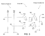
- FIG. 3 illustrates a schematic of one embodiment of a circuit 300 having a resistive divider 301 and a voltage converter 302 .
- the circuit 300 is configured to sense the differential voltage between Vg 206 and Vdd 208 by voltage dividing the voltages using the resistive divider 301 . Different values of resistances may be used for the resistors of the resistor dividers in order to divide down the respective voltages by fractions, such as described above with respect to the divider circuits 230 and 240 .
- the circuit 300 is also configured to perform the differential-to-single-ended conversion using switched capacitor.
- a first transistor T 1 311 is coupled to node 303 of the divided voltage of Vg 208 , and is configured to receive an inverted signal 305 (P 1 B) of a first control signal 306 (P 1 ) at a gate of the first transistor T 1 311 .
- a second transistor T 2 312 is coupled to node 304 of the divided voltage of Vdd 206 , and is configured to receive the inverted signal 305 (P 1 B) at a gate of the second transistor T 2 312 .
- a first capacitor 321 is switched in between the voltage at node 303 and the voltage at node 304 , resulting in the differential voltage between Vg 206 and Vdd 208 .
- the voltage converter 302 includes a third transistor, a fourth transistor and a second capacitor C 2 322 .
- the third transistor T 3 313 is coupled to one end of C 1 321 and one end of the C 2 322 .
- the fourth transistor T 4 314 is coupled to the other end of C 1 321 and ground 203 .
- the second capacitor C 2 322 is coupled between the third transistor T 3 313 and ground 203 .
- the third and fourth transistors are both configured to receive a second control signal at each of their gates, activating the third and fourth transistors to convert the differential voltage on C 1 321 to a single-ended voltage on the second capacitor C 2 322 at the output node 330 , which is referenced to ground 203 .
- One disadvantage of the circuit 300 may be the size of the layout of the circuit 300 .
- the resistive divider 301 on Vg 208 would have to be at least 20 Mega Ohms (MOhms) to limit the load on Vg 208 to the same range as the switched capacitor sampling of Vg 208 illustrated in the circuit 700 of FIG. 6 , resulting in a layout that is more than 50 times larger than the circuit 700 , for example.
- MOhms Mega Ohms
- a capacitive divider may be used, such as illustrated in and described with respect to FIG. 4 .
- FIG. 4 illustrates a schematic of one embodiment of a circuit 400 having a capacitive divider 401 and a voltage converter 402 .
- the circuit 400 is configured to sense the differential voltage between Vg 206 and Vdd 208 by voltage dividing the voltages using the capacitive divider 401 .
- the circuit 400 is also configured to perform the differential-to-single-ended conversion using switched capacitors.
- a first transistor T 1 411 is coupled between node 403 and the voltage Vg 208 .
- the first transistor T 1 411 is a high-voltage transistor.
- a high-voltage transistor is a transistors that is configured to tolerate a high voltage drain-to-source voltage, such as greater than 5.0V.
- High-voltage transistors include a maximum allowable drain-to-source voltage that is greater than approximately 5.0V.
- High-voltage transistors and high voltage signals have been labeled as (HV) in the corresponding figures; otherwise, if the transistors or control signals do not include the (HV) label, the transistors or control signals are not high-voltage transistors or high voltages.
- the high-voltage transistors are configured to tolerate up to approximately 40V drain-to-source voltage. Alternatively, other values may be used.
- the first transistor T 1 (HV) 411 is configured to receive a high-voltage, inverted signal 405 (P 1 B (HV)) of a first control signal 406 (P 1 ) at a gate of the high-voltage, first transistor T 1 411 .
- the inverted signal 405 (P 1 B (HV)) is a high-voltage control signal.
- a low-voltage control signal (P 1 B) is translated to a high-voltage control signal (P 1 B (HV)).
- the circuit 400 also includes a second transistor T 2 412 that is coupled between the node 404 and the voltage Vdd 206 , and is configured to receive the inverted signal 406 (P 1 B) at a gate of the second transistor T 2 412 .
- a first capacitor 421 is switched in between the voltages Vg 206 and Vdd 208 , resulting in the differential voltage between Vg 206 and Vdd 208 on capacitor C 1 421 .
- the differential voltage Vg 206 with respect to Vdd 208 is sampled on C 2 and then referenced to ground (a differential-to-single-ended conversion).
- the signal is divided down by charge sharing with C 2 .
- the output capacitor, C 3 is updated.
- the voltage converter 402 includes a fourth transistor T 4 414 coupled between the node 404 and ground 203 .
- the fourth transistor T 4 414 is configured to receive a second control signal 407 (P 2 ) at a gate of the fourth transistor T 4 414 .
- the control signal 407 activates the fourth transistors to reference the differential voltage between Vg 206 and Vdd 208 to ground 203 .
- the voltage at 403 with respect to ground 203 which represents the value of the differential voltage between Vg 206 and Vdd 208 , is divided down using the capacitive divider 401 .
- the capacitive divider 401 includes a third transistor T 3 (HV) 413 disposed between node 403 and one end of a second capacitor C 2 422 that has the other end coupled to ground 203 .
- the third transistors T 3 (HV) 413 is a high-voltage transistors similar to the first transistor.
- the third transistors T 3 (HV) 413 is configured to receive the second control signal 407 (P 2 ) at a gate of the third transistor.
- the third transistor When the third transistor is activated, charge is shared with the second capacitor C 2 422 .
- the differential voltage can be divided by a fraction.
- the value of the capacitors can be selected to determine the fraction by which the voltage at 403 is divided.
- the output capacitor C 3 423 is updated using a fifth transistor T 5 415 and a sixth transistor T 6 416 .
- the fifth transistor 415 is configured to receive the first control signal 408 (P 1 ) to activate the fifth transistor
- the sixth transistor 416 is configured to receive the second control signal 407 (P 2 ) to activate the sixth transistor.
- the voltage on the second capacitor 422 is updated on the third capacitor C 3 423 at the output node 430 , which is referenced to ground 203 .
- One disadvantage of the circuit 400 may be the generation of high-voltage control signals, such as the inverted signal 405 (P 1 B (HV)) of the first control signal 408 (P 1 ), because a low-voltage control signal needs be translated into a high-voltage control signal.
- Additional circuitry may be used to translate the low-voltage control signal into a high-voltage control signal.
- the additional circuitry that translates the low-voltage control signal (P 1 B) into a high-voltage control signal (P 1 B (HV)) should not draw too much current from Vg 208 , otherwise, the charge pump (e.g., charge pump 280 ) that supplies Vg 208 will need to be increased in size to accommodate the increased load.
- the translation circuit must work for all possible values of Vg 208 , and the high-voltage control signal 405 needs to closely track Vg 208 .
- the control signal 405 e.g., P 1 B (HV)
- the control signal 405 needs to be equal to approximately Vg 208 .
- the control signal 405 needs to be more than 1V below Vg 208 , but not more than 5.5V below Vg 208 to prevent damage to the high-voltage transistor 411 (e.g., high-voltage switch).
- circuit 400 of FIG. 4 may be smaller than the layout of circuit 400 of FIG. 3 using capacitive divider, the circuit 400 of FIG. 4 still includes the disadvantage of controlling a high-voltage transistor using high-voltage control signals, such as control signal 405 (P 1 B (HV)).
- control signal 405 P 1 B (HV)
- Embodiments described below with respect to FIGS. 5 and 6 are directed to controlling a high-voltage transistor (also referred to as high-voltage switch) using low-voltage control signals, instead of high-voltage control signals as described in FIG. 4 .
- FIG. 5 illustrates a schematic of one embodiment of a circuit 500 for controlling a high-voltage switch with low-voltage control signals.
- the illustrated circuit controls a high-voltage transistor (e.g., PFET) with low-voltage control signals 508 (P 1 ) and 507 (P 2 ).
- the circuit 500 includes a first transistor T 1 511 , which has its source coupled to a voltage supply of the voltage Vg 208 .
- the voltage supply is the charge pump 280 .
- other voltage supplies may be used to supply the voltage Vg 208 of FIG. 5 .
- the circuit 500 also includes a second transistor T 2 512 , which has its source also coupled to the voltage Vg 208 .
- the circuit 500 also includes a third transistor T 3 , which has a source coupled to the gates of the first and second transistors 511 and 512 .
- the first transistor T 1 511 , second transistor T 2 512 , and third transistor T 3 513 are high-voltage transistors, and each has a maximum allowable drain-to-source voltage greater than approximately 5.0 volts.
- the third transistor T 3 513 is configured to receive a first control signal 508 (P 1 ) at a gate of the third transistor to turn the first and second transistors 511 and 512 on and off.
- the first control signal 508 (P 1 ), as well as the second control signal 507 (P 2 ), are low-voltage control signals, in that the voltage of the first control signal 508 (P 1 ) can be produced by logic operating at a low voltage.
- the first, second, and third transistors are high-voltage transistors, having a maximum allowable drain-to-source voltage greater than approximately 5.0V; however, unlike the high-voltage transistors of FIG. 4 , the high-voltage transistors of FIG. 5 are controlled using low-voltage control signals (e.g., are less than or equal to approximately 5.0V).
- the circuit 500 also includes a first capacitor C 1 521 coupled between a ground potential 203 and a drain of the third transistor T 3 513 , and a second capacitor C 2 522 coupled between the ground potential 203 and a drain of the first transistor T 1 511 .
- the second capacitor 522 is configured to be charged faster than the first capacitor 521 .
- capacitors C 1 521 and C 2 522 are discharged and T 2 512 and T 3 513 are OFF.
- the low-voltage control signal 508 P 1
- the low-voltage control signal 508 P 1
- the low-voltage control signal 508 P 1
- the low-voltage control signal 508 P 1
- the low-voltage control signal 508 P 1
- the low-voltage control signal 508 P 1
- the low-voltage control signal 508 P 1
- T 3 513 With T 3 513 on, current flows from gate voltage Vg 208 through T 2 512 and T 3 513 onto capacitor C 1 521 . Since the gates of transistors T 1 511 and T 2 512 are connected, transistor T 1 511 (e.g., the high-voltage PFET to be controlled) is also turned on.
- a current twice the size of the first current flows into capacitor C 2 522 due to the 1:2 current mirror configuration.
- the capacitance of the first and second capacitor 521 and 522 are the same, the second capacitor C 2 522 is charged up to the gate voltage Vg 208 before current stops flowing into the first capacitor C 1 521 .
- the first and second capacitors can be configured to be different capacitances so long as the voltage on the second capacitor C 2 522 charges to the gate voltage Vg 208 before current stops flowing into the first capacitors C 1 521 .
- the first control signal 508 is de-activated (e.g., P 1 goes LOW), open circuiting T 3 513 , cutting off current through both branches of the current mirror circuit and turning off T 1 511 and T 2 512 .
- the second control signal 507 P 2 is activated (e.g., P 2 goes HIGH) to discharge the first capacitor C 1 521 , preparing the circuit 500 ready for the next time the first control signal (P 1 ) is activated (e.g., asserted HIGH) to turn on transistors T 1 511 and T 2 512 .
- low-voltage control signals are used to control the switching of a high-voltage switch (e.g., turning on and off the high-voltage transistors.
- the circuit 500 also includes a fifth transistor T 5 515 coupled between the second capacitor C 2 522 and a third capacitor C 3 523 .
- the third capacitor 523 is coupled to the drain of the fifth transistor T 5 515 and the ground potential 203 .
- the fifth transistor T 5 515 is configured to receive the second control signal 507 (P 2 ) at a gate of the fifth transistor to divide a charge on the capacitor C 2 522 at node 503 between the capacitor C 2 522 and the third capacitor C 3 523 .
- the second control signal 507 (P 2 ) is activated (e.g., P 2 goes HIGH) to divide down the voltage on the second capacitor C 2 522 by charge sharing with a third capacitor C 3 523 , as described above with respect to the fifth transistor T 5 515 .
- the gate voltage Vg 208 can be divided by a fraction.
- the value of the capacitors can be selected to determine the fraction by which the voltage at 503 is divided.
- the voltage at node 504 is the divided down voltage using the capacitive voltage divider 502 .
- the circuit 500 also includes a sixth transistor T 6 516 coupled between the capacitor C 3 523 and the ground potential 203 .
- the sixth transistor T 6 516 is configured to receive the first control signal 508 at a gate of the sixth transistor T 6 516 to reset the third capacitor C 3 523 for the subsequent turn on of the sixth transistor node.
- FIG. 5 also illustrates a timing diagram of the first and second control signals 508 and 507 , respectively.
- the first control signal 508 is activated and de-activated first and then the second control signal 507 is activated and de-activated. This process repeats, alternating between activating and de-activating the first and second control signals 508 and 507 , respectively.
- other timing may be accomplished as known by one of ordinary skill in the art.
- the circuit described herein may place a relatively small load current on the gate voltage Vg 208 to obtain control of the high-voltage switch (e.g., first transistor T 1 511 ).
- the circuit achieves control of high-voltage switches with relatively few circuit elements.
- MOSFET metal-oxide-semiconductor field-effect-transistor
- NMOS n-channel MOSFET or PFET or p-channel FET for the high-voltage switch
- Bipolar and BiCMOS complementary metal-oxide-semiconductor field-effect-transistor
- PMOS and CMOS complementary metal-oxide-semiconductor field-effect-transistor
- process technologies for example, Bipolar and BiCMOS
- FIG. 6 illustrates a schematic of one embodiment of a circuit 600 having a capacitive divider 601 and a voltage converter 602 and a circuit 603 for controlling high-voltage transistors using low-voltage control signals.
- Circuit 603 is a similar circuit as described with respect to FIG. 5 , which includes the transistors T 1 -T 4 511 - 514 and the first and second capacitors 521 and 522 .
- the circuit 600 is similar to the circuit 500 , except circuit 600 also includes a switch and a capacitor for sampling and holding the output at node 605 .
- the output at node 605 of FIG. 5 is at ground potential 203 while the first control signal 508 (P 1 ) is HIGH.
- the circuit 603 is coupled to the voltage converter 602 , which include the fifth and sixth transistors T 5 615 and T 6 616 coupled to the other end of the second capacitor 622 .
- the fifth transistor 615 is configured to receive an inverted signal 609 of the first control signal 608 at a gate of the fifth transistor to couple the second capacitor to a voltage potential.
- the voltage potential is the output voltage Vdd 206 , as described with respect to FIG. 2 above. Alternatively, other voltages may be used.
- the sixth transistor 616 is coupled between the second capacitor 622 and the ground potential 203 .
- the sixth transistor 616 is configured to receive the second control signal 607 to convert a differential voltage (Vg-Vdd) between a drain voltage (e.g., Vg 208 ) of the first transistor 611 and the voltage potential (e.g., Vdd 206 ) to a voltage, having a value of the differential voltage, referenced to the ground potential 203 .
- Vg-Vdd a differential voltage between a drain voltage (e.g., Vg 208 ) of the first transistor 611 and the voltage potential (e.g., Vdd 206 ) to a voltage, having a value of the differential voltage, referenced to the ground potential 203 .
- the circuit 603 is also coupled the capacitive divider circuit 601 .
- the capacitive divider circuit 601 includes a seventh transistor T 7 617 coupled to the drain of the first transistor T 1 611 at node 603 and a third capacitor C 3 623 , which is coupled to the ground potential 203 .
- the seventh transistor T 7 617 is configured to receive the second control signal 607 to divide a charge on the second capacitor C 2 622 between the second capacitor 622 and the third capacitor 623 .
- the circuit 600 includes an eighth transistor T 8 618 coupled between the node 604 and the ground potential 203 .
- the eighth transistor T 8 618 is configured to receive the first control signal 608 at a gate of the eighth transistor to reset the third capacitor C 3 623 for the subsequent turn on of the seventh transistor T 7 617 .
- the circuit 600 includes a ninth transistor T 9 619 coupled between the node 604 (one end of the third capacitor C 3 623 ) and the output node 605 , which is at the one end of the fourth capacitor C 4 624 , while the other end is coupled to the ground potential 203 .
- the ninth transistor T 9 619 is configured to receive the second control signal 607 at a gate of the ninth transistor to transfer a charge on the third capacitor C 3 623 to the fourth capacitor C 4 624 .
- the fourth capacitor C 4 624 is configured to store a charge of a previous cycle. Accordingly, when the ninth transistor T 9 619 receives the second control signal 607 at the gate, the ninth transistor T 9 619 is configured to adjust up or adjust down a charge on the fourth capacitor C 4 624 based on the charge of the previous cycle.
- FIG. 6 also illustrates a timing diagram of the first and second control signals 608 and 607 , and the inverted control signal 609 , respectively.
- the first control signal 608 is activated and de-activated first and then the second control signal 607 is activated and de-activated.
- the inverted control signal 609 is the inverted signal of the first control signal 608 .
- P 2 607 is HIGH and P 1 608 is LOW.
- the capacitor C 1 621 is discharged to ground.
- P 1 608 is HIGH and P 2 607 is LOW.
- the C 2 622 Since the second capacitor's 622 bottom plate is connected to the voltage Vdd 206 , the C 2 622 is charged with the differential voltage (e.g., Vgs 216 ) of Vg 208 less Vdd 206 (e.g., Vg ⁇ Vdd).
- the voltage Vgs 216 is gate-to-source voltage of the regulator FET 220 of FIG. 2 .
- the capacitor C 3 623 is discharged to ground.
- the fourth capacitor C 4 624 remains charged to the result of the previous cycle.
- the P 2 607 is HIGH and P 1 608 is LOW.
- the current mirror is off and the C 2 622 is referenced to ground. This performs a differential-to-single-ended conversion.
- the embodiments described above for controlling high-voltage transistors using low-voltage control signals may be used to reduce a current load on the voltage source, such as the charge pump 280 .
- the embodiments described above for controlling high-voltage transistors using low-voltage control signals may be used to reduce die area of the circuit.
- FIG. 7 illustrates a flow chart of one embodiment of a method 700 for disabling an internal voltage regulator of a circuit to voltage stress test the circuit.
- Method 700 includes providing a circuit having an internal voltage regulator, operation 701 , and disabling the internal voltage regulator to voltage stress test the circuit, operation 702 .
- operation 702 although the internal voltage regulator is no longer regulating, the internal voltage regulator functions as a switch connecting the high voltage supply to the internal supply voltage and causes the gate-to-source voltage of the regulating FET to be equal to the internal supply voltage.
- the method 700 may also include voltage stress testing the circuit, operation 703 , and/or voltage stress testing a gate oxide of the regulator FET of the internal voltage regulator, operation 704 .
- the method includes applying a voltage to the internal core block that is higher than a maximum voltage allowed by the internal voltage regulator.
- the operation of disabling the internal voltage regulator includes sensing the gate-to-source voltage Vgs of the regulator FET, sensing a voltage (Vdd) applied to the internal core block, comparing the voltage Vdd and the Vgs, and controlling the Vgs of the regulator FET, based on the comparison of the voltage Vdd and the Vgs, to allow the voltage Vdd applied to the internal core block to be higher than a maximum voltage allowed by the internal voltage regulator.
- the method 700 includes selecting at least one of a test mode of operation or a normal mode of operation.
- the operation of disabling the internal voltage regulator of the circuit includes disabling the internal voltage regulator while in the test mode.
- FIG. 8 illustrates a flow chart of one embodiment of a method 800 for controlling a high-voltage transistor using low-voltage control signals.
- Method 800 includes providing a first transistor having a source coupled to a first voltage supply (e.g., high-voltage supply that is greater than 5.0V), operation 801 .
- the first transistor has a maximum allowable drain-to-source voltage greater than approximately 5.0 volts.
- the method 800 also includes controlling (e.g., turning on and off) the first transistor with first and second low-voltage control signals (e.g., less than or equal to 5.0V), operation 802 .
- the first and second low-voltage control signals may be produced by logic operating on a second voltage supply that is a low-voltage supply (e.g., 5V or less) relative to the first voltage supply (e.g., high-voltage supply).
- the maximum voltage of the first and second control signals is less than the maximum allowable drain-to-source voltage of the first transistor.
- the method 800 also includes turning on the first transistor by providing a second transistor (high-voltage transistor) having a source coupled to the first voltage supply (e.g., high-voltage supply), operation 803 .
- the operation of turning on the first transistor includes receiving the first control signal at a gate of a third transistor, which is coupled to the gates of the first and second transistors, to turn on the first and second transistors, operation 804 .
- the operation of turning on the first transistor includes charging a first capacitor at a first rate while the first transistor is turned on, operation 805 .
- the operation of turning on the first transistor also includes charging a second capacitor at a second rate, which is faster than the first rate, while the second transistor is turned on, operation 806 .
- the method 800 also includes turning off the first transistor by de-asserting the first control signal at the gate of the third transistor to turn off the first and second transistors, operation 807 .
- the operation of turning off the first transistor also includes receiving the second control signal at a gate of a fourth transistor having a source coupled to the drain of the third transistor, operation 808 , and discharging the first capacitor for a subsequent turn on of the first and second transistors while the fourth transistor is turned on, operation 809 .
- the operation of turning off the first transistor may also include receiving an inverted signal of the first control signal at a gate of a fifth transistor to couple the second capacitor to a voltage potential, receiving the second control signal at a gate of a sixth transistor to activate the sixth transistor, and converting a differential voltage between a drain voltage of the first transistor and the voltage potential to a voltage with respect to ground when the sixth transistor is activated.
- the inverted signal may be produced by logic operating on the second voltage supply (e.g., low-voltage supply).
- the operation of turning off the first transistor may also include receiving the second control signal at a gate of a seventh transistor to activate the seventh transistor, and dividing a charge on the second capacitor between the second capacitor and a third capacitors that is coupled to a drain of the seventh capacitor and the ground potential when the seventh transistor is activated.
- the embodiments described above with respect to controlling a high-voltage transistor using low-voltage control signals may be used to reduce a current load on a voltage supply, such as a charge pump.
- the embodiments described above may be used to reduce the die area of the circuit.
- Embodiments of the present invention include various operations. These operations may be performed by hardware components, software, firmware, or a combination thereof.
- the term “coupled to” may mean coupled directly or indirectly through one or more intervening components. Any of the signals provided over various buses described herein may be time multiplexed with other signals and provided over one or more common buses. Additionally, the interconnection between circuit components or blocks may be shown as buses or as single signal lines. Each of the buses may alternatively be one or more single signal lines and each of the single signal lines may alternatively be buses.
Landscapes
- Engineering & Computer Science (AREA)
- Computer Hardware Design (AREA)
- Microelectronics & Electronic Packaging (AREA)
- General Engineering & Computer Science (AREA)
- Physics & Mathematics (AREA)
- General Physics & Mathematics (AREA)
- Semiconductor Integrated Circuits (AREA)
Abstract
Description
| parameter | |||||
| actively | |||||
| HVPWR | Vds | Vdd | Vgs | Vg | controlled |
| 36 V | 31 V | 5.0 V | 1.0 V | 6.0 V | Vdd |
| 5.5 V | 0.5 V | 5.0 V | 1.0 V | 6.0 V | Vdd |
| 4.0 V | 0.1 V | 3.9 V | 4.0 V | 7.9 V | Vgs |
| 2.5 V | 0.1 V | 2.4 V | 4.0 V | 6.4 V | Vgs |
| parameter | |||||
| actively | |||||
| HVPWR | Vds | Vdd | Vgs | Vg | controlled |
| 36 V | 0.1 V | 6.9 V | 6.9 V | 13.8 V | Vgs |
| 5.5 V | 0.1 V | 5.9 V | 5.4 V | 10.8 V | Vgs |
| 4.0 V | 0.1 V | 3.9 V | 3.9 V | 7.8 V | Vgs |
| 2.5 V | 0.1 V | 2.4 V | 2.4 V | 4.8 V | Vgs |
Claims (13)
Priority Applications (1)
| Application Number | Priority Date | Filing Date | Title |
|---|---|---|---|
| US11/705,986 US7705600B1 (en) | 2006-02-13 | 2007-02-12 | Voltage stress testing of core blocks and regulator transistors |
Applications Claiming Priority (3)
| Application Number | Priority Date | Filing Date | Title |
|---|---|---|---|
| US77300106P | 2006-02-13 | 2006-02-13 | |
| US77300006P | 2006-02-13 | 2006-02-13 | |
| US11/705,986 US7705600B1 (en) | 2006-02-13 | 2007-02-12 | Voltage stress testing of core blocks and regulator transistors |
Publications (1)
| Publication Number | Publication Date |
|---|---|
| US7705600B1 true US7705600B1 (en) | 2010-04-27 |
Family
ID=42112469
Family Applications (1)
| Application Number | Title | Priority Date | Filing Date |
|---|---|---|---|
| US11/705,986 Expired - Fee Related US7705600B1 (en) | 2006-02-13 | 2007-02-12 | Voltage stress testing of core blocks and regulator transistors |
Country Status (1)
| Country | Link |
|---|---|
| US (1) | US7705600B1 (en) |
Cited By (9)
| Publication number | Priority date | Publication date | Assignee | Title |
|---|---|---|---|---|
| ITMI20111139A1 (en) * | 2011-06-23 | 2012-12-24 | St Microelectronics Srl | ELECTRONIC CIRCUIT AND METHOD TO TEST AND KEEP A MOS TRANSISTOR OFF |
| US8598891B2 (en) | 2009-10-20 | 2013-12-03 | Analog Devices, Inc. | Detection and mitigation of particle contaminants in MEMS devices |
| US9588171B2 (en) | 2012-05-16 | 2017-03-07 | Infineon Technologies Ag | System and method for testing an integrated circuit |
| US9804207B1 (en) * | 2016-03-01 | 2017-10-31 | Xilinx, Inc. | Internal voltage monitoring for integrated circuit devices |
| US10481204B2 (en) * | 2010-12-24 | 2019-11-19 | Intel Corporation | Methods and systems to measure a signal on an integrated circuit die |
| CN115033043A (en) * | 2021-03-03 | 2022-09-09 | 圣邦微电子(北京)股份有限公司 | Testing device for low dropout regulator |
| US11531064B2 (en) | 2020-11-04 | 2022-12-20 | Stmicroelectronics S.R.L. | Method for testing a digital electronic circuit to be tested, corresponding test system and computer program product |
| US11824548B2 (en) * | 2021-12-17 | 2023-11-21 | Xilinx, Inc. | Pulse generator for injection locked oscillator |
| CN119105598A (en) * | 2023-06-09 | 2024-12-10 | 意法半导体国际公司 | Power supply sequence independent high voltage regulator disable circuit |
Citations (27)
| Publication number | Priority date | Publication date | Assignee | Title |
|---|---|---|---|---|
| US4217610A (en) | 1978-09-25 | 1980-08-12 | Tektronix, Inc. | Variable start multiburst signal generator |
| US5086280A (en) | 1990-03-12 | 1992-02-04 | Mitsubishi Denki Kabushiki Kaisha | Continuously variable pulsewidth waveform formation device employing two memories |
| US5124573A (en) | 1990-12-20 | 1992-06-23 | International Business Machines | Adjustable clock chopper/expander circuit |
| JPH04227314A (en) | 1990-04-16 | 1992-08-17 | Sony Tektronix Corp | digital delay circuit |
| US5202640A (en) * | 1991-06-03 | 1993-04-13 | International Business Machines Corporation | Capacitance and leakage test method and apparatus |
| US5410195A (en) | 1991-10-31 | 1995-04-25 | Nec Corporation | Ripple-free phase detector using two sample-and-hold circuits |
| US5452253A (en) * | 1992-09-24 | 1995-09-19 | Goldstar Electron, Co. Ltd. | Burn-in test circuit for semiconductor memory device |
| US5610546A (en) | 1992-12-09 | 1997-03-11 | Texas Instruments Incorporated | Controlled delay circuit |
| US5621355A (en) | 1995-09-29 | 1997-04-15 | Harris Corporation | Sampled data-biasing of continuous time integrated circuit |
| US5767719A (en) | 1993-11-25 | 1998-06-16 | Nec Corporation | Delay circuit using capacitor and transistor |
| US5848010A (en) * | 1997-07-14 | 1998-12-08 | Micron Technology, Inc. | Circuit and method for antifuse stress test |
| US5909398A (en) * | 1994-08-19 | 1999-06-01 | Kabushiki Kaisha Toshiba | Semiconductor memory device and high-voltage switching circuit |
| US6043717A (en) | 1998-09-22 | 2000-03-28 | Intel Corporation | Signal synchronization and frequency synthesis system configurable as PLL or DLL |
| US6100739A (en) | 1998-09-09 | 2000-08-08 | Cypress Semiconductor Corp. | Self-timed synchronous pulse generator with test mode |
| US6175928B1 (en) | 1997-12-31 | 2001-01-16 | Intel Corporation | Reducing timing variance of signals from an electronic device |
| US6327318B1 (en) | 1998-06-30 | 2001-12-04 | Mosaid Technologies Incorporated | Process, voltage, temperature independent switched delay compensation scheme |
| US6445238B1 (en) | 1999-12-01 | 2002-09-03 | Xilinx, Inc. | Method and apparatus for adjusting delay in a delay locked loop for temperature variations |
| US6445661B1 (en) | 1999-08-11 | 2002-09-03 | Oak Technology, Inc. | Circuit, disk controller and method for calibrating a high precision delay of an input signal |
| US6650105B2 (en) * | 2000-08-07 | 2003-11-18 | Vanguard International Semiconductor Corporation | EPROM used as a voltage monitor for semiconductor burn-in |
| US6747492B2 (en) | 2002-06-18 | 2004-06-08 | Koninklijke Philips Electronics N.V. | Power-on reset circuit with current shut-off and semiconductor device including the same |
| US6819157B2 (en) | 2001-07-02 | 2004-11-16 | Lucent Technologies Inc. | Delay compensation circuit |
| US6917236B2 (en) | 1999-09-30 | 2005-07-12 | Interuniversitair Micro-Elektronica Centrum (Imec Vzw) | Method and apparatus for level shifting |
| US7019576B1 (en) | 2003-03-24 | 2006-03-28 | Cypress Semiconductor Corporation | Delay circuit that scales with clock cycle time |
| US7265495B2 (en) | 2002-12-19 | 2007-09-04 | Matsushita Electric Industrial Co., Ltd. | Display driver |
| US7323923B2 (en) | 2004-08-30 | 2008-01-29 | Matsushita Electric Industrial Co., Ltd. | Driver circuit |
| US7428675B2 (en) * | 2003-02-20 | 2008-09-23 | International Business Machines Corporation | Testing using independently controllable voltage islands |
| US7456885B2 (en) | 2003-08-22 | 2008-11-25 | Micron Technology, Inc. | Per column one-bit ADC for image sensors |
-
2007
- 2007-02-12 US US11/705,986 patent/US7705600B1/en not_active Expired - Fee Related
Patent Citations (28)
| Publication number | Priority date | Publication date | Assignee | Title |
|---|---|---|---|---|
| US4217610A (en) | 1978-09-25 | 1980-08-12 | Tektronix, Inc. | Variable start multiburst signal generator |
| US5086280A (en) | 1990-03-12 | 1992-02-04 | Mitsubishi Denki Kabushiki Kaisha | Continuously variable pulsewidth waveform formation device employing two memories |
| JPH04227314A (en) | 1990-04-16 | 1992-08-17 | Sony Tektronix Corp | digital delay circuit |
| US5124573A (en) | 1990-12-20 | 1992-06-23 | International Business Machines | Adjustable clock chopper/expander circuit |
| US5202640A (en) * | 1991-06-03 | 1993-04-13 | International Business Machines Corporation | Capacitance and leakage test method and apparatus |
| US5410195A (en) | 1991-10-31 | 1995-04-25 | Nec Corporation | Ripple-free phase detector using two sample-and-hold circuits |
| US5452253A (en) * | 1992-09-24 | 1995-09-19 | Goldstar Electron, Co. Ltd. | Burn-in test circuit for semiconductor memory device |
| US5610546A (en) | 1992-12-09 | 1997-03-11 | Texas Instruments Incorporated | Controlled delay circuit |
| US5767719A (en) | 1993-11-25 | 1998-06-16 | Nec Corporation | Delay circuit using capacitor and transistor |
| US5909398A (en) * | 1994-08-19 | 1999-06-01 | Kabushiki Kaisha Toshiba | Semiconductor memory device and high-voltage switching circuit |
| US5621355A (en) | 1995-09-29 | 1997-04-15 | Harris Corporation | Sampled data-biasing of continuous time integrated circuit |
| US5848010A (en) * | 1997-07-14 | 1998-12-08 | Micron Technology, Inc. | Circuit and method for antifuse stress test |
| US6009029A (en) * | 1997-07-14 | 1999-12-28 | Micron Technology, Inc. | Circuit and method for antifuse stress test |
| US6175928B1 (en) | 1997-12-31 | 2001-01-16 | Intel Corporation | Reducing timing variance of signals from an electronic device |
| US6327318B1 (en) | 1998-06-30 | 2001-12-04 | Mosaid Technologies Incorporated | Process, voltage, temperature independent switched delay compensation scheme |
| US6100739A (en) | 1998-09-09 | 2000-08-08 | Cypress Semiconductor Corp. | Self-timed synchronous pulse generator with test mode |
| US6043717A (en) | 1998-09-22 | 2000-03-28 | Intel Corporation | Signal synchronization and frequency synthesis system configurable as PLL or DLL |
| US6445661B1 (en) | 1999-08-11 | 2002-09-03 | Oak Technology, Inc. | Circuit, disk controller and method for calibrating a high precision delay of an input signal |
| US6917236B2 (en) | 1999-09-30 | 2005-07-12 | Interuniversitair Micro-Elektronica Centrum (Imec Vzw) | Method and apparatus for level shifting |
| US6445238B1 (en) | 1999-12-01 | 2002-09-03 | Xilinx, Inc. | Method and apparatus for adjusting delay in a delay locked loop for temperature variations |
| US6650105B2 (en) * | 2000-08-07 | 2003-11-18 | Vanguard International Semiconductor Corporation | EPROM used as a voltage monitor for semiconductor burn-in |
| US6819157B2 (en) | 2001-07-02 | 2004-11-16 | Lucent Technologies Inc. | Delay compensation circuit |
| US6747492B2 (en) | 2002-06-18 | 2004-06-08 | Koninklijke Philips Electronics N.V. | Power-on reset circuit with current shut-off and semiconductor device including the same |
| US7265495B2 (en) | 2002-12-19 | 2007-09-04 | Matsushita Electric Industrial Co., Ltd. | Display driver |
| US7428675B2 (en) * | 2003-02-20 | 2008-09-23 | International Business Machines Corporation | Testing using independently controllable voltage islands |
| US7019576B1 (en) | 2003-03-24 | 2006-03-28 | Cypress Semiconductor Corporation | Delay circuit that scales with clock cycle time |
| US7456885B2 (en) | 2003-08-22 | 2008-11-25 | Micron Technology, Inc. | Per column one-bit ADC for image sensors |
| US7323923B2 (en) | 2004-08-30 | 2008-01-29 | Matsushita Electric Industrial Co., Ltd. | Driver circuit |
Non-Patent Citations (11)
| Title |
|---|
| U.S. Appl. No. 09/150,551: "Self-Timed Synchronous Pulse Generator with Test Mode," Ansel et al., filed on Sep. 9, 1998; 18 pages. |
| U.S. Appl. No. 10/804,988: "Delay Circuit that Scales with Clock Cycle Time," Sancheti et al.,filed on Mar. 18, 2004; 26 pages. |
| U.S. Appl. No. 11/705,985; "Controlling a High-Voltage Switch with Low-Voltage Control Signals," Bruce Byrkett, filed on Feb. 12, 2007; 48 pages. |
| USPTO Advisory Action for U.S. Appl. No. 11/705,985 dated Apr. 10, 2009; 3 pages. |
| USPTO Final Rejection for U.S. Appl. No. 11/705,985 dated Feb. 6, 2009; 7 pages. |
| USPTO Non-Final Rejection for U.S. Appl. No. 09/150,551 dated Nov. 12, 1999; 7 pages. |
| USPTO Non-Final Rejection for U.S. Appl. No. 11/705,985 dated Sep. 10, 2008; 7 pages. |
| USPTO Notice of Allowance for U.S. Appl. No. 09/150,551 dated Mar. 24, 2000; 5 pages. |
| USPTO Notice of Allowance for U.S. Appl. No. 10/804,988 dated Jun. 8, 2005; 7 pages. |
| USPTO Notice of Allowance for U.S. Appl. No. 10/804,988 dated Oct. 20, 2005; 7 pages. |
| USPTO Notice of Allowance for U.S. Appl. No. 11/705,985 dated May 14, 2009; 7 pages. |
Cited By (15)
| Publication number | Priority date | Publication date | Assignee | Title |
|---|---|---|---|---|
| US8598891B2 (en) | 2009-10-20 | 2013-12-03 | Analog Devices, Inc. | Detection and mitigation of particle contaminants in MEMS devices |
| US10481204B2 (en) * | 2010-12-24 | 2019-11-19 | Intel Corporation | Methods and systems to measure a signal on an integrated circuit die |
| US9024652B2 (en) | 2011-06-23 | 2015-05-05 | Stmicroelectronics S.R.L. | Electronic circuit and method for testing and keeping a MOS transistor switched-off |
| ITMI20111139A1 (en) * | 2011-06-23 | 2012-12-24 | St Microelectronics Srl | ELECTRONIC CIRCUIT AND METHOD TO TEST AND KEEP A MOS TRANSISTOR OFF |
| US9588171B2 (en) | 2012-05-16 | 2017-03-07 | Infineon Technologies Ag | System and method for testing an integrated circuit |
| US10288669B2 (en) | 2012-05-16 | 2019-05-14 | Infineon Technologies Ag | System and method for testing an integrated circuit |
| DE102013209068B4 (en) | 2012-05-16 | 2022-06-15 | Infineon Technologies Ag | System and method for testing an integrated circuit |
| US9804207B1 (en) * | 2016-03-01 | 2017-10-31 | Xilinx, Inc. | Internal voltage monitoring for integrated circuit devices |
| US11531064B2 (en) | 2020-11-04 | 2022-12-20 | Stmicroelectronics S.R.L. | Method for testing a digital electronic circuit to be tested, corresponding test system and computer program product |
| CN115033043A (en) * | 2021-03-03 | 2022-09-09 | 圣邦微电子(北京)股份有限公司 | Testing device for low dropout regulator |
| US11824548B2 (en) * | 2021-12-17 | 2023-11-21 | Xilinx, Inc. | Pulse generator for injection locked oscillator |
| CN119105598A (en) * | 2023-06-09 | 2024-12-10 | 意法半导体国际公司 | Power supply sequence independent high voltage regulator disable circuit |
| EP4474950A1 (en) * | 2023-06-09 | 2024-12-11 | STMicroelectronics International N.V. | Supply sequence independent high-voltage tolerant regulator disable circuit |
| US20240413742A1 (en) * | 2023-06-09 | 2024-12-12 | Stmicroelectronics International N.V. | Supply sequence independent high-voltage tolerant regulator disable circuit |
| US12519387B2 (en) * | 2023-06-09 | 2026-01-06 | Stmicroelectronics International N.V. | Supply sequence independent high-voltage tolerant regulator disable circuit |
Similar Documents
| Publication | Publication Date | Title |
|---|---|---|
| US7705600B1 (en) | Voltage stress testing of core blocks and regulator transistors | |
| US7969203B1 (en) | Switch-body PMOS switch with switch-body dummies | |
| US9722593B2 (en) | Gate driver circuit | |
| US7061217B2 (en) | Integrated power switching circuit | |
| US20090040671A1 (en) | Power clamp for on-chip ESD protection | |
| CN113271090B (en) | Sampling switch circuit | |
| US12155300B2 (en) | Input dependent common mode biasing | |
| US8830095B2 (en) | Track and hold circuit and method | |
| US10122359B2 (en) | Integrated circuit control of anti-series switches | |
| US8988117B2 (en) | Gate-stress test circuit without test pad | |
| KR100528858B1 (en) | Amplitude converting circuit | |
| EP2330741A2 (en) | Switch-body PMOS switch with switch-body dummies | |
| JP2013191911A (en) | Analog switch | |
| US20110148473A1 (en) | Switch-body pmos switch with switch-body dummies | |
| US20090039924A1 (en) | Systems and methods for reducing distortion in semiconductor based sampling systems | |
| US6927592B2 (en) | Device for monitoring quiescent current of an electronic device | |
| US7130225B1 (en) | Charge pump with large bypass capacitors | |
| US10277223B2 (en) | Charge injection compensation circuit | |
| JP2000132989A (en) | Track hold circuit | |
| US20250362699A1 (en) | Load drive circuit | |
| US20240195297A1 (en) | Voltage booster including circuitry to reduce overvoltage stress on discharge protection device | |
| US12339693B2 (en) | Circuit and system for actively discharging a power stage input node during power supply turn-on | |
| US10186942B2 (en) | Methods and apparatus for discharging a node of an electrical circuit | |
| US20250337405A1 (en) | Electronic switching module and method of controlling such a module | |
| US20250141442A1 (en) | High voltage tolerant bootstrap switch |
Legal Events
| Date | Code | Title | Description |
|---|---|---|---|
| AS | Assignment |
Owner name: CYPRESS SEMICONDUCTOR CORPORATION,CALIFORNIA Free format text: ASSIGNMENT OF ASSIGNORS INTEREST;ASSIGNOR:BYRKETT, BRUCE;REEL/FRAME:018962/0152 Effective date: 20070209 |
|
| FEPP | Fee payment procedure |
Free format text: PAYER NUMBER DE-ASSIGNED (ORIGINAL EVENT CODE: RMPN); ENTITY STATUS OF PATENT OWNER: LARGE ENTITY Free format text: PAYOR NUMBER ASSIGNED (ORIGINAL EVENT CODE: ASPN); ENTITY STATUS OF PATENT OWNER: LARGE ENTITY |
|
| STCF | Information on status: patent grant |
Free format text: PATENTED CASE |
|
| FPAY | Fee payment |
Year of fee payment: 4 |
|
| AS | Assignment |
Owner name: MORGAN STANLEY SENIOR FUNDING, INC., NEW YORK Free format text: SECURITY INTEREST;ASSIGNORS:CYPRESS SEMICONDUCTOR CORPORATION;SPANSION LLC;REEL/FRAME:035240/0429 Effective date: 20150312 |
|
| FEPP | Fee payment procedure |
Free format text: PAYER NUMBER DE-ASSIGNED (ORIGINAL EVENT CODE: RMPN); ENTITY STATUS OF PATENT OWNER: LARGE ENTITY Free format text: PAYOR NUMBER ASSIGNED (ORIGINAL EVENT CODE: ASPN); ENTITY STATUS OF PATENT OWNER: LARGE ENTITY |
|
| AS | Assignment |
Owner name: MONTEREY RESEARCH, LLC, CALIFORNIA Free format text: ASSIGNMENT OF ASSIGNORS INTEREST;ASSIGNOR:CYPRESS SEMICONDUCTOR CORPORATION;REEL/FRAME:042108/0880 Effective date: 20170322 |
|
| AS | Assignment |
Owner name: CYPRESS SEMICONDUCTOR CORPORATION, CALIFORNIA Free format text: RELEASE BY SECURED PARTY;ASSIGNOR:MORGAN STANLEY SENIOR FUNDING, INC.;REEL/FRAME:042769/0227 Effective date: 20170322 |
|
| MAFP | Maintenance fee payment |
Free format text: PAYMENT OF MAINTENANCE FEE, 8TH YEAR, LARGE ENTITY (ORIGINAL EVENT CODE: M1552) Year of fee payment: 8 |
|
| AS | Assignment |
Owner name: MORGAN STANLEY SENIOR FUNDING, INC., NEW YORK Free format text: CORRECTIVE ASSIGNMENT TO CORRECT THE 8647899 PREVIOUSLY RECORDED ON REEL 035240 FRAME 0429. ASSIGNOR(S) HEREBY CONFIRMS THE SECURITY INTERST;ASSIGNORS:CYPRESS SEMICONDUCTOR CORPORATION;SPANSION LLC;REEL/FRAME:058002/0470 Effective date: 20150312 |
|
| FEPP | Fee payment procedure |
Free format text: MAINTENANCE FEE REMINDER MAILED (ORIGINAL EVENT CODE: REM.); ENTITY STATUS OF PATENT OWNER: LARGE ENTITY |
|
| LAPS | Lapse for failure to pay maintenance fees |
Free format text: PATENT EXPIRED FOR FAILURE TO PAY MAINTENANCE FEES (ORIGINAL EVENT CODE: EXP.); ENTITY STATUS OF PATENT OWNER: LARGE ENTITY |
|
| STCH | Information on status: patent discontinuation |
Free format text: PATENT EXPIRED DUE TO NONPAYMENT OF MAINTENANCE FEES UNDER 37 CFR 1.362 |
|
| FP | Lapsed due to failure to pay maintenance fee |
Effective date: 20220427 |