US7705376B2 - Sensor and method of manufacturing the same - Google Patents
Sensor and method of manufacturing the same Download PDFInfo
- Publication number
- US7705376B2 US7705376B2 US11/270,568 US27056805A US7705376B2 US 7705376 B2 US7705376 B2 US 7705376B2 US 27056805 A US27056805 A US 27056805A US 7705376 B2 US7705376 B2 US 7705376B2
- Authority
- US
- United States
- Prior art keywords
- semiconductor film
- mesopores
- oxide
- gas
- sensor
- Prior art date
- Legal status (The legal status is an assumption and is not a legal conclusion. Google has not performed a legal analysis and makes no representation as to the accuracy of the status listed.)
- Expired - Fee Related, expires
Links
- 238000004519 manufacturing process Methods 0.000 title description 12
- 239000004065 semiconductor Substances 0.000 claims abstract description 107
- 239000011368 organic material Substances 0.000 claims abstract description 38
- 238000000034 method Methods 0.000 claims description 41
- 239000000126 substance Substances 0.000 claims description 21
- 238000001179 sorption measurement Methods 0.000 claims description 15
- VYPSYNLAJGMNEJ-UHFFFAOYSA-N Silicium dioxide Chemical group O=[Si]=O VYPSYNLAJGMNEJ-UHFFFAOYSA-N 0.000 claims description 14
- 229910052814 silicon oxide Inorganic materials 0.000 claims description 11
- 238000009826 distribution Methods 0.000 claims description 10
- 238000002441 X-ray diffraction Methods 0.000 claims description 8
- 238000003795 desorption Methods 0.000 claims description 5
- 230000004044 response Effects 0.000 claims description 5
- 238000004611 spectroscopical analysis Methods 0.000 claims 1
- 239000007789 gas Substances 0.000 description 166
- 239000011148 porous material Substances 0.000 description 134
- 239000010408 film Substances 0.000 description 99
- 239000000758 substrate Substances 0.000 description 63
- XOLBLPGZBRYERU-UHFFFAOYSA-N tin dioxide Chemical compound O=[Sn]=O XOLBLPGZBRYERU-UHFFFAOYSA-N 0.000 description 62
- 239000002245 particle Substances 0.000 description 60
- 229910001887 tin oxide Inorganic materials 0.000 description 58
- 239000010409 thin film Substances 0.000 description 50
- 239000000243 solution Substances 0.000 description 46
- 239000004094 surface-active agent Substances 0.000 description 40
- BASFCYQUMIYNBI-UHFFFAOYSA-N platinum Chemical compound [Pt] BASFCYQUMIYNBI-UHFFFAOYSA-N 0.000 description 38
- QPLDLSVMHZLSFG-UHFFFAOYSA-N Copper oxide Chemical compound [Cu]=O QPLDLSVMHZLSFG-UHFFFAOYSA-N 0.000 description 37
- KDLHZDBZIXYQEI-UHFFFAOYSA-N Palladium Chemical compound [Pd] KDLHZDBZIXYQEI-UHFFFAOYSA-N 0.000 description 35
- 238000006243 chemical reaction Methods 0.000 description 34
- 229910010272 inorganic material Inorganic materials 0.000 description 24
- 239000011147 inorganic material Substances 0.000 description 24
- 230000008859 change Effects 0.000 description 22
- 229910044991 metal oxide Inorganic materials 0.000 description 21
- 150000004706 metal oxides Chemical class 0.000 description 21
- 239000001257 hydrogen Substances 0.000 description 16
- 229910052739 hydrogen Inorganic materials 0.000 description 16
- 238000005259 measurement Methods 0.000 description 16
- UGFAIRIUMAVXCW-UHFFFAOYSA-N Carbon monoxide Chemical compound [O+]#[C-] UGFAIRIUMAVXCW-UHFFFAOYSA-N 0.000 description 15
- UFHFLCQGNIYNRP-UHFFFAOYSA-N Hydrogen Chemical compound [H][H] UFHFLCQGNIYNRP-UHFFFAOYSA-N 0.000 description 15
- 239000012298 atmosphere Substances 0.000 description 15
- 229910002091 carbon monoxide Inorganic materials 0.000 description 15
- 229910052697 platinum Inorganic materials 0.000 description 14
- 230000008569 process Effects 0.000 description 14
- LFQSCWFLJHTTHZ-UHFFFAOYSA-N Ethanol Chemical compound CCO LFQSCWFLJHTTHZ-UHFFFAOYSA-N 0.000 description 13
- 229910052763 palladium Inorganic materials 0.000 description 13
- 150000002736 metal compounds Chemical class 0.000 description 12
- 239000013081 microcrystal Substances 0.000 description 12
- 239000002243 precursor Substances 0.000 description 12
- 238000001514 detection method Methods 0.000 description 10
- 230000035945 sensitivity Effects 0.000 description 10
- 229910052751 metal Inorganic materials 0.000 description 9
- 239000002184 metal Substances 0.000 description 9
- VNWKTOKETHGBQD-UHFFFAOYSA-N methane Chemical compound C VNWKTOKETHGBQD-UHFFFAOYSA-N 0.000 description 9
- IJGRMHOSHXDMSA-UHFFFAOYSA-N Atomic nitrogen Chemical compound N#N IJGRMHOSHXDMSA-UHFFFAOYSA-N 0.000 description 8
- 239000006087 Silane Coupling Agent Substances 0.000 description 8
- 239000010949 copper Substances 0.000 description 8
- 229910001873 dinitrogen Inorganic materials 0.000 description 8
- -1 for instance Chemical compound 0.000 description 8
- 239000000463 material Substances 0.000 description 8
- 239000002904 solvent Substances 0.000 description 7
- QGZKDVFQNNGYKY-UHFFFAOYSA-N Ammonia Chemical compound N QGZKDVFQNNGYKY-UHFFFAOYSA-N 0.000 description 6
- 238000000862 absorption spectrum Methods 0.000 description 6
- 229920001400 block copolymer Polymers 0.000 description 6
- 239000006185 dispersion Substances 0.000 description 6
- 238000001035 drying Methods 0.000 description 6
- 230000007613 environmental effect Effects 0.000 description 6
- 238000012360 testing method Methods 0.000 description 6
- RYGMFSIKBFXOCR-UHFFFAOYSA-N Copper Chemical compound [Cu] RYGMFSIKBFXOCR-UHFFFAOYSA-N 0.000 description 5
- RWSOTUBLDIXVET-UHFFFAOYSA-N Dihydrogen sulfide Chemical compound S RWSOTUBLDIXVET-UHFFFAOYSA-N 0.000 description 5
- 239000007864 aqueous solution Substances 0.000 description 5
- 229910052802 copper Inorganic materials 0.000 description 5
- YYLGKUPAFFKGRQ-UHFFFAOYSA-N dimethyldiethoxysilane Chemical compound CCO[Si](C)(C)OCC YYLGKUPAFFKGRQ-UHFFFAOYSA-N 0.000 description 5
- 230000004048 modification Effects 0.000 description 5
- 238000012986 modification Methods 0.000 description 5
- XLYOFNOQVPJJNP-UHFFFAOYSA-N water Substances O XLYOFNOQVPJJNP-UHFFFAOYSA-N 0.000 description 5
- YQUVCSBJEUQKSH-UHFFFAOYSA-N 3,4-dihydroxybenzoic acid Chemical compound OC(=O)C1=CC=C(O)C(O)=C1 YQUVCSBJEUQKSH-UHFFFAOYSA-N 0.000 description 4
- MWUXSHHQAYIFBG-UHFFFAOYSA-N Nitric oxide Chemical compound O=[N] MWUXSHHQAYIFBG-UHFFFAOYSA-N 0.000 description 4
- 239000011248 coating agent Substances 0.000 description 4
- 238000000576 coating method Methods 0.000 description 4
- DTPCFIHYWYONMD-UHFFFAOYSA-N decaethylene glycol Polymers OCCOCCOCCOCCOCCOCCOCCOCCOCCOCCO DTPCFIHYWYONMD-UHFFFAOYSA-N 0.000 description 4
- 125000000524 functional group Chemical group 0.000 description 4
- 239000010931 gold Substances 0.000 description 4
- 150000002431 hydrogen Chemical class 0.000 description 4
- 229910000037 hydrogen sulfide Inorganic materials 0.000 description 4
- 239000002923 metal particle Substances 0.000 description 4
- NWAHZABTSDUXMJ-UHFFFAOYSA-N platinum(2+);dinitrate Chemical compound [Pt+2].[O-][N+]([O-])=O.[O-][N+]([O-])=O NWAHZABTSDUXMJ-UHFFFAOYSA-N 0.000 description 4
- 238000011946 reduction process Methods 0.000 description 4
- 239000005751 Copper oxide Substances 0.000 description 3
- OKKJLVBELUTLKV-UHFFFAOYSA-N Methanol Chemical compound OC OKKJLVBELUTLKV-UHFFFAOYSA-N 0.000 description 3
- 229910002651 NO3 Inorganic materials 0.000 description 3
- PXHVJJICTQNCMI-UHFFFAOYSA-N Nickel Chemical compound [Ni] PXHVJJICTQNCMI-UHFFFAOYSA-N 0.000 description 3
- XUIMIQQOPSSXEZ-UHFFFAOYSA-N Silicon Chemical compound [Si] XUIMIQQOPSSXEZ-UHFFFAOYSA-N 0.000 description 3
- YXFVVABEGXRONW-UHFFFAOYSA-N Toluene Chemical compound CC1=CC=CC=C1 YXFVVABEGXRONW-UHFFFAOYSA-N 0.000 description 3
- 238000004458 analytical method Methods 0.000 description 3
- 230000005540 biological transmission Effects 0.000 description 3
- 230000000052 comparative effect Effects 0.000 description 3
- 229910000431 copper oxide Inorganic materials 0.000 description 3
- 239000013078 crystal Substances 0.000 description 3
- 238000002425 crystallisation Methods 0.000 description 3
- 230000008025 crystallization Effects 0.000 description 3
- 238000003618 dip coating Methods 0.000 description 3
- 125000002887 hydroxy group Chemical group [H]O* 0.000 description 3
- 150000002941 palladium compounds Chemical class 0.000 description 3
- 150000003058 platinum compounds Chemical class 0.000 description 3
- 239000010453 quartz Substances 0.000 description 3
- 229910052710 silicon Inorganic materials 0.000 description 3
- 239000010703 silicon Substances 0.000 description 3
- 150000003606 tin compounds Chemical class 0.000 description 3
- HPGGPRDJHPYFRM-UHFFFAOYSA-J tin(iv) chloride Chemical compound Cl[Sn](Cl)(Cl)Cl HPGGPRDJHPYFRM-UHFFFAOYSA-J 0.000 description 3
- VEXZGXHMUGYJMC-UHFFFAOYSA-M Chloride anion Chemical compound [Cl-] VEXZGXHMUGYJMC-UHFFFAOYSA-M 0.000 description 2
- ATJFFYVFTNAWJD-UHFFFAOYSA-N Tin Chemical compound [Sn] ATJFFYVFTNAWJD-UHFFFAOYSA-N 0.000 description 2
- 229910021626 Tin(II) chloride Inorganic materials 0.000 description 2
- 238000010521 absorption reaction Methods 0.000 description 2
- 239000002253 acid Substances 0.000 description 2
- 150000001298 alcohols Chemical class 0.000 description 2
- QVGXLLKOCUKJST-UHFFFAOYSA-N atomic oxygen Chemical compound [O] QVGXLLKOCUKJST-UHFFFAOYSA-N 0.000 description 2
- 150000004653 carbonic acids Chemical class 0.000 description 2
- 239000011651 chromium Substances 0.000 description 2
- 230000000694 effects Effects 0.000 description 2
- 239000007772 electrode material Substances 0.000 description 2
- 239000012530 fluid Substances 0.000 description 2
- PCHJSUWPFVWCPO-UHFFFAOYSA-N gold Chemical compound [Au] PCHJSUWPFVWCPO-UHFFFAOYSA-N 0.000 description 2
- 229910052737 gold Inorganic materials 0.000 description 2
- 238000007654 immersion Methods 0.000 description 2
- 239000007788 liquid Substances 0.000 description 2
- 239000011572 manganese Substances 0.000 description 2
- 239000000693 micelle Substances 0.000 description 2
- 238000002156 mixing Methods 0.000 description 2
- 229910000480 nickel oxide Inorganic materials 0.000 description 2
- 239000010955 niobium Substances 0.000 description 2
- 239000002736 nonionic surfactant Substances 0.000 description 2
- 230000003647 oxidation Effects 0.000 description 2
- 238000007254 oxidation reaction Methods 0.000 description 2
- 239000001301 oxygen Substances 0.000 description 2
- 229910052760 oxygen Inorganic materials 0.000 description 2
- MUJIDPITZJWBSW-UHFFFAOYSA-N palladium(2+) Chemical compound [Pd+2] MUJIDPITZJWBSW-UHFFFAOYSA-N 0.000 description 2
- PIBWKRNGBLPSSY-UHFFFAOYSA-L palladium(II) chloride Chemical compound Cl[Pd]Cl PIBWKRNGBLPSSY-UHFFFAOYSA-L 0.000 description 2
- YJVFFLUZDVXJQI-UHFFFAOYSA-L palladium(ii) acetate Chemical compound [Pd+2].CC([O-])=O.CC([O-])=O YJVFFLUZDVXJQI-UHFFFAOYSA-L 0.000 description 2
- 238000000206 photolithography Methods 0.000 description 2
- 238000002360 preparation method Methods 0.000 description 2
- 150000003377 silicon compounds Chemical class 0.000 description 2
- 235000011150 stannous chloride Nutrition 0.000 description 2
- 239000013076 target substance Substances 0.000 description 2
- CMCBDXRRFKYBDG-UHFFFAOYSA-N 1-dodecoxydodecane Chemical compound CCCCCCCCCCCCOCCCCCCCCCCCC CMCBDXRRFKYBDG-UHFFFAOYSA-N 0.000 description 1
- FDCJDKXCCYFOCV-UHFFFAOYSA-N 1-hexadecoxyhexadecane Chemical compound CCCCCCCCCCCCCCCCOCCCCCCCCCCCCCCCC FDCJDKXCCYFOCV-UHFFFAOYSA-N 0.000 description 1
- HBXWUCXDUUJDRB-UHFFFAOYSA-N 1-octadecoxyoctadecane Chemical compound CCCCCCCCCCCCCCCCCCOCCCCCCCCCCCCCCCCCC HBXWUCXDUUJDRB-UHFFFAOYSA-N 0.000 description 1
- HANWHVWXFQSQGJ-UHFFFAOYSA-N 1-tetradecoxytetradecane Chemical compound CCCCCCCCCCCCCCOCCCCCCCCCCCCCC HANWHVWXFQSQGJ-UHFFFAOYSA-N 0.000 description 1
- SJECZPVISLOESU-UHFFFAOYSA-N 3-trimethoxysilylpropan-1-amine Chemical compound CO[Si](OC)(OC)CCCN SJECZPVISLOESU-UHFFFAOYSA-N 0.000 description 1
- IKHGUXGNUITLKF-UHFFFAOYSA-N Acetaldehyde Chemical compound CC=O IKHGUXGNUITLKF-UHFFFAOYSA-N 0.000 description 1
- QGZKDVFQNNGYKY-UHFFFAOYSA-O Ammonium Chemical compound [NH4+] QGZKDVFQNNGYKY-UHFFFAOYSA-O 0.000 description 1
- CURLTUGMZLYLDI-UHFFFAOYSA-N Carbon dioxide Chemical compound O=C=O CURLTUGMZLYLDI-UHFFFAOYSA-N 0.000 description 1
- VYZAMTAEIAYCRO-UHFFFAOYSA-N Chromium Chemical compound [Cr] VYZAMTAEIAYCRO-UHFFFAOYSA-N 0.000 description 1
- IAYPIBMASNFSPL-UHFFFAOYSA-N Ethylene oxide Chemical compound C1CO1 IAYPIBMASNFSPL-UHFFFAOYSA-N 0.000 description 1
- 238000005033 Fourier transform infrared spectroscopy Methods 0.000 description 1
- 229910002621 H2PtCl6 Inorganic materials 0.000 description 1
- 238000004566 IR spectroscopy Methods 0.000 description 1
- XEEYBQQBJWHFJM-UHFFFAOYSA-N Iron Chemical compound [Fe] XEEYBQQBJWHFJM-UHFFFAOYSA-N 0.000 description 1
- 239000002879 Lewis base Substances 0.000 description 1
- PWHULOQIROXLJO-UHFFFAOYSA-N Manganese Chemical compound [Mn] PWHULOQIROXLJO-UHFFFAOYSA-N 0.000 description 1
- CBENFWSGALASAD-UHFFFAOYSA-N Ozone Chemical compound [O-][O+]=O CBENFWSGALASAD-UHFFFAOYSA-N 0.000 description 1
- YGYAWVDWMABLBF-UHFFFAOYSA-N Phosgene Chemical class ClC(Cl)=O YGYAWVDWMABLBF-UHFFFAOYSA-N 0.000 description 1
- ZLMJMSJWJFRBEC-UHFFFAOYSA-N Potassium Chemical compound [K] ZLMJMSJWJFRBEC-UHFFFAOYSA-N 0.000 description 1
- KJTLSVCANCCWHF-UHFFFAOYSA-N Ruthenium Chemical compound [Ru] KJTLSVCANCCWHF-UHFFFAOYSA-N 0.000 description 1
- BQCADISMDOOEFD-UHFFFAOYSA-N Silver Chemical compound [Ag] BQCADISMDOOEFD-UHFFFAOYSA-N 0.000 description 1
- 229910021627 Tin(IV) chloride Inorganic materials 0.000 description 1
- XLOMVQKBTHCTTD-UHFFFAOYSA-N Zinc monoxide Chemical compound [Zn]=O XLOMVQKBTHCTTD-UHFFFAOYSA-N 0.000 description 1
- 238000005299 abrasion Methods 0.000 description 1
- 150000001299 aldehydes Chemical class 0.000 description 1
- 150000001408 amides Chemical class 0.000 description 1
- 150000001412 amines Chemical class 0.000 description 1
- 125000003277 amino group Chemical group 0.000 description 1
- 229940045985 antineoplastic platinum compound Drugs 0.000 description 1
- 238000003491 array Methods 0.000 description 1
- AQBOUNVXZQRXNP-UHFFFAOYSA-L azane;dichloropalladium Chemical compound N.N.N.N.Cl[Pd]Cl AQBOUNVXZQRXNP-UHFFFAOYSA-L 0.000 description 1
- WIDMMNCAAAYGKW-UHFFFAOYSA-N azane;palladium(2+);dinitrate Chemical compound N.N.N.N.[Pd+2].[O-][N+]([O-])=O.[O-][N+]([O-])=O WIDMMNCAAAYGKW-UHFFFAOYSA-N 0.000 description 1
- 230000008901 benefit Effects 0.000 description 1
- 150000001718 carbodiimides Chemical class 0.000 description 1
- 125000002915 carbonyl group Chemical group [*:2]C([*:1])=O 0.000 description 1
- 238000005266 casting Methods 0.000 description 1
- 239000003054 catalyst Substances 0.000 description 1
- 230000003197 catalytic effect Effects 0.000 description 1
- 239000000919 ceramic Substances 0.000 description 1
- 239000007795 chemical reaction product Substances 0.000 description 1
- 150000001805 chlorine compounds Chemical class 0.000 description 1
- 229910052804 chromium Inorganic materials 0.000 description 1
- 229910017052 cobalt Inorganic materials 0.000 description 1
- 239000010941 cobalt Substances 0.000 description 1
- GUTLYIVDDKVIGB-UHFFFAOYSA-N cobalt atom Chemical compound [Co] GUTLYIVDDKVIGB-UHFFFAOYSA-N 0.000 description 1
- IVMYJDGYRUAWML-UHFFFAOYSA-N cobalt(ii) oxide Chemical compound [Co]=O IVMYJDGYRUAWML-UHFFFAOYSA-N 0.000 description 1
- 238000002485 combustion reaction Methods 0.000 description 1
- 238000000354 decomposition reaction Methods 0.000 description 1
- 238000000151 deposition Methods 0.000 description 1
- 238000004070 electrodeposition Methods 0.000 description 1
- 238000005530 etching Methods 0.000 description 1
- RTZKZFJDLAIYFH-UHFFFAOYSA-N ether Substances CCOCC RTZKZFJDLAIYFH-UHFFFAOYSA-N 0.000 description 1
- 239000011521 glass Substances 0.000 description 1
- 229910052736 halogen Inorganic materials 0.000 description 1
- 150000002367 halogens Chemical class 0.000 description 1
- 238000010438 heat treatment Methods 0.000 description 1
- 229910052809 inorganic oxide Inorganic materials 0.000 description 1
- 230000001788 irregular Effects 0.000 description 1
- 150000002576 ketones Chemical class 0.000 description 1
- 150000007527 lewis bases Chemical class 0.000 description 1
- 229910052748 manganese Inorganic materials 0.000 description 1
- 239000011859 microparticle Substances 0.000 description 1
- 239000012046 mixed solvent Substances 0.000 description 1
- MJVUDZGNBKFOBF-UHFFFAOYSA-N n-nitronitramide Chemical compound [O-][N+](=O)N[N+]([O-])=O MJVUDZGNBKFOBF-UHFFFAOYSA-N 0.000 description 1
- 229910052759 nickel Inorganic materials 0.000 description 1
- 229910052758 niobium Inorganic materials 0.000 description 1
- GUCVJGMIXFAOAE-UHFFFAOYSA-N niobium atom Chemical compound [Nb] GUCVJGMIXFAOAE-UHFFFAOYSA-N 0.000 description 1
- URLJKFSTXLNXLG-UHFFFAOYSA-N niobium(5+);oxygen(2-) Chemical compound [O-2].[O-2].[O-2].[O-2].[O-2].[Nb+5].[Nb+5] URLJKFSTXLNXLG-UHFFFAOYSA-N 0.000 description 1
- 150000002826 nitrites Chemical class 0.000 description 1
- 125000000449 nitro group Chemical group [O-][N+](*)=O 0.000 description 1
- 230000001590 oxidative effect Effects 0.000 description 1
- GNRSAWUEBMWBQH-UHFFFAOYSA-N oxonickel Chemical compound [Ni]=O GNRSAWUEBMWBQH-UHFFFAOYSA-N 0.000 description 1
- GPNDARIEYHPYAY-UHFFFAOYSA-N palladium(ii) nitrate Chemical compound [Pd+2].[O-][N+]([O-])=O.[O-][N+]([O-])=O GPNDARIEYHPYAY-UHFFFAOYSA-N 0.000 description 1
- 239000004033 plastic Substances 0.000 description 1
- 239000002985 plastic film Substances 0.000 description 1
- 229920006255 plastic film Polymers 0.000 description 1
- 229920001296 polysiloxane Polymers 0.000 description 1
- 229910052700 potassium Inorganic materials 0.000 description 1
- 239000011591 potassium Substances 0.000 description 1
- 238000012545 processing Methods 0.000 description 1
- CCTFOFUMSKSGRK-UHFFFAOYSA-N propan-2-olate;tin(4+) Chemical compound [Sn+4].CC(C)[O-].CC(C)[O-].CC(C)[O-].CC(C)[O-] CCTFOFUMSKSGRK-UHFFFAOYSA-N 0.000 description 1
- 238000011160 research Methods 0.000 description 1
- 239000011347 resin Substances 0.000 description 1
- 229920005989 resin Polymers 0.000 description 1
- 230000004043 responsiveness Effects 0.000 description 1
- 229910052707 ruthenium Inorganic materials 0.000 description 1
- 229910052709 silver Inorganic materials 0.000 description 1
- 239000004332 silver Substances 0.000 description 1
- 150000003384 small molecules Chemical class 0.000 description 1
- 238000002336 sorption--desorption measurement Methods 0.000 description 1
- 238000001228 spectrum Methods 0.000 description 1
- 238000004528 spin coating Methods 0.000 description 1
- 238000005507 spraying Methods 0.000 description 1
- 238000004544 sputter deposition Methods 0.000 description 1
- 150000003457 sulfones Chemical class 0.000 description 1
- 150000003462 sulfoxides Chemical class 0.000 description 1
- JBQYATWDVHIOAR-UHFFFAOYSA-N tellanylidenegermanium Chemical compound [Te]=[Ge] JBQYATWDVHIOAR-UHFFFAOYSA-N 0.000 description 1
- FPADWGFFPCNGDD-UHFFFAOYSA-N tetraethoxystannane Chemical compound [Sn+4].CC[O-].CC[O-].CC[O-].CC[O-] FPADWGFFPCNGDD-UHFFFAOYSA-N 0.000 description 1
- 150000003568 thioethers Chemical class 0.000 description 1
- 150000003573 thiols Chemical class 0.000 description 1
- WFKWXMTUELFFGS-UHFFFAOYSA-N tungsten Chemical compound [W] WFKWXMTUELFFGS-UHFFFAOYSA-N 0.000 description 1
- 229910052721 tungsten Inorganic materials 0.000 description 1
- 239000010937 tungsten Substances 0.000 description 1
- ZNOKGRXACCSDPY-UHFFFAOYSA-N tungsten trioxide Chemical compound O=[W](=O)=O ZNOKGRXACCSDPY-UHFFFAOYSA-N 0.000 description 1
- 238000007738 vacuum evaporation Methods 0.000 description 1
- LEONUFNNVUYDNQ-UHFFFAOYSA-N vanadium atom Chemical compound [V] LEONUFNNVUYDNQ-UHFFFAOYSA-N 0.000 description 1
Images


Classifications
-
- G—PHYSICS
- G01—MEASURING; TESTING
- G01N—INVESTIGATING OR ANALYSING MATERIALS BY DETERMINING THEIR CHEMICAL OR PHYSICAL PROPERTIES
- G01N27/00—Investigating or analysing materials by the use of electric, electrochemical, or magnetic means
- G01N27/02—Investigating or analysing materials by the use of electric, electrochemical, or magnetic means by investigating impedance
- G01N27/04—Investigating or analysing materials by the use of electric, electrochemical, or magnetic means by investigating impedance by investigating resistance
- G01N27/12—Investigating or analysing materials by the use of electric, electrochemical, or magnetic means by investigating impedance by investigating resistance of a solid body in dependence upon absorption of a fluid; of a solid body in dependence upon reaction with a fluid, for detecting components in the fluid
-
- Y—GENERAL TAGGING OF NEW TECHNOLOGICAL DEVELOPMENTS; GENERAL TAGGING OF CROSS-SECTIONAL TECHNOLOGIES SPANNING OVER SEVERAL SECTIONS OF THE IPC; TECHNICAL SUBJECTS COVERED BY FORMER USPC CROSS-REFERENCE ART COLLECTIONS [XRACs] AND DIGESTS
- Y10—TECHNICAL SUBJECTS COVERED BY FORMER USPC
- Y10T—TECHNICAL SUBJECTS COVERED BY FORMER US CLASSIFICATION
- Y10T428/00—Stock material or miscellaneous articles
- Y10T428/249921—Web or sheet containing structurally defined element or component
- Y10T428/249953—Composite having voids in a component [e.g., porous, cellular, etc.]
- Y10T428/249967—Inorganic matrix in void-containing component
- Y10T428/249969—Of silicon-containing material [e.g., glass, etc.]
-
- Y—GENERAL TAGGING OF NEW TECHNOLOGICAL DEVELOPMENTS; GENERAL TAGGING OF CROSS-SECTIONAL TECHNOLOGIES SPANNING OVER SEVERAL SECTIONS OF THE IPC; TECHNICAL SUBJECTS COVERED BY FORMER USPC CROSS-REFERENCE ART COLLECTIONS [XRACs] AND DIGESTS
- Y10—TECHNICAL SUBJECTS COVERED BY FORMER USPC
- Y10T—TECHNICAL SUBJECTS COVERED BY FORMER US CLASSIFICATION
- Y10T428/00—Stock material or miscellaneous articles
- Y10T428/249921—Web or sheet containing structurally defined element or component
- Y10T428/249953—Composite having voids in a component [e.g., porous, cellular, etc.]
- Y10T428/249967—Inorganic matrix in void-containing component
- Y10T428/24997—Of metal-containing material
Definitions
- the present invention relates to a sensor for detecting a substance that is adsorbed to and/or desorbed from the surface of semiconductor and a method of manufacturing the same.
- This invention can be applied to a gas sensor and a bio sensor.
- semiconductor type sensors are adapted to detect a substance, utilizing a metal oxide semiconductor having a property of changing its resistance in response to adsorption or desorption of the substance.
- semiconductor type sensors find applications in gas escape alarms and so on.
- Oxide semiconductors, tin oxide in particular, are popularly used for gas sensors.
- One of the challenges to existing gas sensor elements is selective detection of a gas as an object of detection.
- the width of the depletion layer that is present on the surface of the metal oxide changes, as a function of the adsorption or desorption.
- metal oxide semiconductor elements that are used in gas sensor elements are mostly devised to detect the change in the electric resistance of the semiconductor element.
- oxygen molecules adsorbed to the surface of tin oxide are removed as a result of a chemical reaction (combustion) of a gas and the oxygen adsorbed to the surface of tin oxide, and consequently the width of the depletion layer is reduced to by turn lower the electric resistance of the tin oxide.
- the above object is achieved by providing a sensor comprising: a semiconductor film having a plurality of mesopores and containing an oxide; and electrodes electrically connected to the semiconductor film; at least part of surfaces in the mesopores being coated with an organic material.
- a sensor comprising: a semiconductor film having a plurality of mesopores and containing an oxide; and electrodes electrically connected to the semiconductor film; at least part of surfaces in the mesopores being coated with an oxide different from said oxide.
- a sensor comprising: a semiconductor film having a plurality of mesopores and containing a tin oxide; and electrodes electrically connected to the semiconductor film; particles of an inorganic material being held in the mesopores.
- a method of manufacturing a sensor comprising: preparing a reaction solution containing a metal compound and a surfactant and applying the reaction solution onto a substrate; holding the substrate with the reaction solution applied thereto in a steam-containing atmosphere and forming a film containing a metal oxide and the surfactant on the substrate; removing the surfactant from the film and producing a film having a plurality of mesopores; and causing the mesopores to hold particles of an inorganic material.
- a method of manufacturing a sensor comprising: preparing a reaction solution containing a metal compound and a surfactant and applying the reaction solution onto a substrate; holding the substrate with the reaction solution applied thereto in a steam-containing atmosphere and forming a film containing a metal oxide and the surfactant on the substrate; removing the surfactant from the film and producing a film having a plurality of mesopores; and coating at least part of surfaces in the mesopores with an organic material.
- a method of manufacturing a sensor comprising: preparing a reaction solution containing a metal compound and a surfactant and applying the reaction solution onto a substrate; holding the substrate with the reaction solution applied thereto in a steam-containing atmosphere and forming a film containing a metal oxide and the surfactant on the substrate; removing the surfactant from the film and producing a film having a plurality of mesopores; and coating at least part of surfaces in the mesopores with an inorganic oxide.
- the present invention can provide a sensor that can selectively detect molecules of a specific gas.
- FIG. 1 is a schematic perspective view of a sensor according to the invention, showing its configuration
- FIG. 2 is a schematic cross sectional view of the sensor of FIG. 1 ;
- FIG. 3 is an enlarged schematic view of a mesopore in FIG. 2 ;
- FIG. 4 is an enlarged schematic view of a mesopore in FIG. 2 ;
- FIG. 5 is an enlarged schematic view of a mesopore in FIG. 2 ;
- FIGS. 6A , 6 B, 6 C and 6 D are schematic illustrations of particles of an inorganic material
- FIG. 7 is a schematic cross sectional view of an embodiment of sensor according to the invention.
- FIG. 8 is a schematic cross sectional view of another embodiment of sensor according to the invention.
- FIG. 9 is a schematic illustration of an arrangement of mesopores
- FIG. 10 is a flowchart of a method of manufacturing a sensor according to the invention.
- FIG. 11 is a schematic illustration of an apparatus for evaluating the characteristics of a sensor according to the invention.
- FIG. 12 is a graph illustrating the changes in the electric resistance observed when a plurality of gases is detected by means of a sensor according to the invention.
- FIG. 13 is a graph illustrating, the changes in the electric resistance observed when a plurality of gases is detected by means of a sensor prepared for the purpose of comparison with a sensor according to the invention
- FIG. 14 is a graph illustrating the changes in the electric resistance observed when a plurality of gases are detected by means of a sensor according to the invention.
- FIG. 15 is a graph illustrating the changes in the electric resistance observed when a plurality of gases are detected by means of a sensor element prepared for the purpose of comparison with a sensor according to the invention
- FIG. 16 is a graph illustrating the changes with time in the electric resistance observed when a plurality of gases are detected by means of a sensor according to the invention.
- FIG. 17 is a graph illustrating the changes with time in the electric resistance observed when a plurality of gases are detected by means of a known sensor for the purpose of comparison.
- FIGS. 1 , 2 , 3 , 4 and 5 will be described in detail. Firstly, the present invention will by summarily described by referring to FIGS. 1 , 2 , 3 , 4 and 5 .
- FIG. 1 is a schematic perspective view of a sensor according to the invention, showing its configuration.
- a pair of electrodes 12 , 12 is arranged on a substrate 13 and a porous oxide semiconductor film 11 is formed thereon as a sensing section.
- FIG. 2 is a schematic cross sectional view of the sensor of FIG. 1 taken along line 2 - 2 .
- a pair of electrodes 12 , 12 and a porous oxide semiconductor film 11 are formed on the substrate 13 .
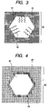
- the porous oxide semiconductor film 11 has a plurality of mesopores 14 . While mesopores will be described in detail hereinafter, FIGS. 3 , 4 and 5 provide enlarged views of mesopores.
- FIG. 3 , 4 and 5 provide enlarged views of mesopores.
- FIG. 3 is an enlarged schematic view of a mesopore, showing that the surface in the mesopore is coated with an organic material.
- FIG. 4 is another enlarged schematic view of a mesopore, showing that the surface in the mesopore is coated with an oxide different from the oxide contained in the porous oxide semiconductor film 11 .
- FIG. 5 is still another enlarged schematic view of a mesopore, showing that particles of an inorganic material are held in the mesopore.
- a sensor according to the present invention is so devised as to be capable of selectively detecting gas molecules by coating the surfaces in the mesopores or causing the surfaces in the mesopores to hold particles of an inorganic material.
- a “mesopore” is defined to be a pore with a pore size between 2 nm and 50 nm according to the classification of IUPAC.
- a pore with a pore size less than 2 nm is defined to be a micropore, while a pore with a pore size greater than 50 nm is defined to be a macropore.
- the specific surface area is smaller in a structure having macropores whose sizes are larger than those of mesopores than in a structure having a plurality of mesopores.
- a structure having a smaller specific surface area can hold a lesser amount of particles of an inorganic material or a lesser amount of an oxide of an organic material in the pores. Additionally, such a structure can adsorb a lesser amount of gas molecules to be detected.
- a structure having mesopores can most suitably be used for a gas sensor or a bio sensor to detect small molecules.
- a “porous oxide semiconductor film” is preferably a continuous film. Such a film can show a higher efficiency of utilization and a higher response speed than a porous oxide semiconductor film 11 that is formed as an aggregate of particles when used for a sensor.
- the porous oxide semiconductor film 11 is an aggregate of particles in a structure, the structure shows a smaller specific surface area than a structure having mesopores. Then, the efficiency of utilization of the element may not become high and the response speed may be low when it is used for a sensor.
- the “oxide contained in the porous oxide semiconductor film” is preferably a metal oxide that shows characteristics of semiconductor.
- metal oxides that show such characteristics include tin oxide (SnO 2 ), zinc oxide (ZnO), niobium oxide (Nb 2 O 5 ) and tungsten oxide (WO 3 ), of which tin oxide (SnO 2 ) can preferably be used for the purpose of the present invention.
- organic material that can selectively catch the detection substance, or the detection substances, and change the electric resistance of the metal oxide may be used.
- organic materials containing one or more than one Lewis bases are preferable candidates.
- Such organic materials have any of the functional groups and bonds listed below as examples.
- Examples of functional groups include halogens, alcohols, amines, nitrites, nitros, sulfides, sulfoxides, sulfones, thiols, carbonyls, aldehydes, ketones, carbonic acids, amides, carbonic acid chlorides, carbonic acid anhydride and organic carbonic acids.
- bonds examples include ether bonds, ester bonds and amide bonds.
- the “oxide different from the oxide contained in the porous oxide semiconductor film 11 ” may be any oxide that can selectively separate a specific gas or reacts with a specific gas and can change the electric resistance of the porous oxide semiconductor film.
- oxides include silicon oxide. Silicon oxide selectively allows a gas having a small molecular weight to pass through it. More specifically, silicon oxide selectively allows hydrogen to pass through it so that it can be used for a hydrogen sensor.
- Particles of an inorganic material may be those of any material that can separate or decompose the detection substance from gas or liquid containing the detection substance by means of a catalytic effect.
- inorganic materials that can be used for the purpose of the present invention include palladium (Pd), platinum (Pt), ruthenium (Ru), silver (Ag), cobalt (Co), gold (Au), nickel (Ni), copper (Cu), manganese (Mn), iron (Fe), chromium (Cr) and vanadium (V).
- palladium (Pd) and platinum (Pt) are preferable because they show an excellent selectivity relative to hydrogen gas.
- Particles of any metal oxide having a similar effect may also be used.
- metal oxides include copper oxide (II) (CuO), nickel oxide (NiO) and cobalt oxide (CoO), of which copper oxide (II) (CuO) may preferably be used for a sensor for detecting hydrogen sulfide because it is highly selective relative to hydrogen sulfide.
- Particles of an inorganic material may show any profile so long as they can be introduced into pores.
- they may show any of the profiles illustrated in FIGS. 6A , 6 B, 6 C and 6 D that include spherical ( FIG. 6A ), wire-shaped ( FIG. 6B ), rod-shaped ( FIG. 6C ) and tubular ( FIG. 6D .).
- Particles of an inorganic material may have any size so long as they can be held in pores to prevent gas from diffusing into the pores. If particles of an inorganic material are spherical, it is preferable that their sizes are smaller than the sizes of the pores.
- Electrodes may be comb-like electrodes as shown in FIG. 1 that may be realized by bonding a plurality of electrodes.
- an arrangement where a plurality of electrodes are formed on the porous oxide semiconductor film as shown in FIG. 7 or an arrangement where electrodes are formed on and under the porous oxide semiconductor film as shown in FIG. 8 may be used for the purpose of the present invention.
- the electrodes are connected to an electric circuit to measure the change in the electric resistance of the porous material and determine if there is the detection substance, or the target substance to be detected.
- a heater and/or microcrystals may be used and the arrangement and the pore sizes of mesopores (fine pores) may be defined in a manner as described below.
- a heater may be arranged in order to accelerate the adsorption/desorption reaction of the detection substance and heat the substrate and the porous oxide semiconductor film. On a cold site, it is convenient to set the temperature of the sensor optimally for the reaction with gas.
- a heater is preferably arranged at a position where it is held in contact with the porous oxide semiconductor film, although some other layer may be disposed between the porous oxide semiconductor film and the heater.
- FIG. 9 shows mesopores that are arranged to show a two-dimensional hexagonal structure.
- the arrangement of fine pores is not limited to such a structure.
- they may alternatively be arranged to show a distorted two-dimensional hexagonal structure, a cubic structure or a three-dimensional hexagonal structure.
- the fine pores may have a unique size or different sizes that do not show any clear periodicity.
- the porous oxide semiconductor film 11 preferably shows one or more than one diffraction peaks in the angular region that corresponds to the structural periodicity of not less than 1 nm in X-ray diffraction analysis. This is because the pore arrays in the porous oxide semiconductor film shows a regular structural periodicity, mesopores are densely arranged to raise the specific surface area thereof in the porous oxide semiconductor film.
- a technique for measuring adsorption isotherms of gas such as nitrogen gas is generally used to evaluate the distribution of fine pores in a porous oxide semiconductor film 11 and the distribution of fine pores are computationally determined from the obtained adsorption isotherms typically by means of the Berret-Joyner-Halenda (BJH) analysis method.
- gas such as nitrogen gas
- the distribution of fine pores of a porous oxide semiconductor film 11 to be used for the purpose of the invention are determined by the BJH method from the data obtained by observing the nitrogen gas adsorption of the fine pores. It is preferable that the distribution of fine pore diameters shows a unique maximum value and not less than 60% of the diameters of the fine pores are found within a range not greater than 12 nm.
- the pore walls of the porous oxide semiconductor film 11 preferably contain microcrystals.
- tin oxide it was found as a result of a series of intensive researches conducted by the inventors of the present invention on the correlation between the particle diameters of tin oxide and the sensitivity of detecting the detection substance that an enhanced level of sensitivity can be achieved when the diameters of micro-particles are not greater than 10 nm, particularly when the diameters are not greater than 6 nm.
- the diameters of microcrystals can be controlled by controlling the conditions of the processing step using steam and the step of removing the surfactant, which will be described in greater detail hereinafter.
- FIG. 10 is a flowchart of a method of manufacturing a porous oxide semiconductor film for the purpose of the present invention.
- Step A is a step of preparing a reaction solution containing a metal compound and a surfactant and applying the reaction solution onto a substrate.
- Step B is a step of holding the substrate, to which the reaction solution has been applied, in a steam-containing atmosphere and forming a film containing the metal oxide and the surfactant.
- Step C is a step of removing the surfactant from the film and forming a plurality of mesopores.
- Step D 1 is a step of part of surfaces in the mesopores with an organic material or an oxide.
- Step D 2 is a step of holding particles of an inorganic material in the mesopores.
- a filmy precursor of a porous oxide semiconductor film that is made of an aggregate of the surfactant and has a region that subsequently makes mesopores is formed on the substrate.
- Such a structure is prepared by the process that the surfactant produces a micelle on the substrate to operate as a mold for producing mesopores (fine pores) and the metal compound forms the walls of the fine pores.
- Step B As the precursor of the porous oxide semiconductor film is held in a steam-containing atmosphere in Step B, the regularity of the fine pore structure of the precursor of the porous oxide semiconductor film is improved and, at the same time, the oxide semiconductor that is amorphous immediately after the application of the reaction solution is induced to become crystallized by steam.
- the surfactant is removed and a porous oxide semiconductor film is produced as a result of carrying out the Step C.
- the sensor becomes provided with the function of selectively detecting the detection substance as a result of modifying the film surface and the pore surfaces of the porous oxide semiconductor film and holding particles of the inorganic material in the pores as a result of carrying out Steps D 1 and D 2 .
- electrodes may be formed on the porous oxide semiconductor film for the purpose of detecting the change in the electric resistance of the porous oxide semiconductor film.
- the electrodes may be formed in any of the above-described steps, after Steps D 1 and D 2 or before Step A so long as the electrodes can be connected to the porous oxide semiconductor film.
- Step A Step of Preparing a Reaction Solution Containing a Metal Compound and a Surfactant and Applying the Reaction Solution Onto a Substrate
- Step A firstly a reaction solution containing a metal compound and a surfactant is prepared.
- the metal compound is a material for preparing an oxide semiconductor and contains, for example, tin (Sn), zinc (Zn), tungsten (W) or niobium (Nb). Particularly, a metal compound containing tin is preferably used.
- reaction solution will be described in terms of a tin compound.
- Tin compounds that can be used for the purpose of the present invention include chlorides such as tin chloride (I) (SnCl 2 ) and tin chloride (II) (SnCl 4 ) and tin alkoxides such as tin isopropoxide and tin ethoxide, although tin compounds that can be used for the purpose of the present invention are not limited to those listed above.
- the surfactant produces a micelle that operates as a mold for producing fine pores.
- a non-ionic surfactant is preferably used for the surfactant.
- Non-ionic surfactants containing ethylene oxide are particularly preferable.
- examples of such surfactants include the following:
- triblock coplymers are preferably used.
- alcohols such as methanol and ethanol are preferable candidate of solvent
- a mixed solvent of alcohol and water can also be used.
- any solvent that is liquid and can dissolve the metal compound and the surfactant may be used for the purpose of the present invention. Acid or the like may be appropriately added to the solvent as catalyst.
- reaction solution is prepared in a manner as described above.
- the prepared reaction solution is then applied onto a substrate.
- a substrate that is chemically stable relative to the reaction solution and hence hardly chemically reacts with the reaction solution is preferably used.
- substrates include glass substrates, ceramic substrates, resin substrates and metal substrates.
- flexible film such as plastic film may also be used for the substrate.
- the electrodes and the porous material can be connected with ease after Steps B and C, which will be described hereinafter, by using a substrate on which electrodes are formed as shown in FIGS. 1 and 2 .
- Examples of effective techniques that can be used for applying the reaction solution onto the substrate easily in a short period of time include the casting, dip coating and spin coating.
- reaction solution is applied onto the substrate in the above-described manner. Note, however, that it is preferable to dry the reaction solution (particularly solvent) on the substrate after Step A and before Step B.
- Step A it is preferable to carry out a drying step of drying the solvent in a temperature range between 25 and 50° C. and a humidity range between 10 and 30% before moving to Step B.
- Step B Holding the Substrate, to which the Reaction Solution has been Applied, in a Steam-containing Atmosphere and Forming a Film Containing the Metal Oxide and the Surfactant on the Substrate
- the substrate which the reaction solution has been applied to and dried is held in a steam-containing atmosphere and a precursor of a porous oxide semiconductor film is formed.
- the relative humidity of the steam-containing atmosphere of Step B is preferably not lower than 40% and not higher than 100% and the temperature of the steam-containing atmosphere is preferably not higher than 100° C.
- the duration of the above process using steam may be appropriately determined according to the level of crystallinity to be achieved.
- Step C Removing the Surfactant From the Film and Forming a Plurality of Mesopores
- a baking process of applying heat to the surfactant to decompose and remove it is preferable because it is simple and provides an advantage of accelerating the crystallization of the oxide semiconductor present on the fine pore walls.
- the surfactant When the surfactant is extracted by means of a supercritical fluid or a solvent, it is possible to hold the density of hydroxyl groups on the pore surfaces to a high level after removing the surfactant. As a result, it is possible to improve the density of the modification using the organic material.
- the surfactant can be decomposed and removed by means of other techniques such as irradiation of UV rays and oxidation/decomposition by ozone.
- techniques that can be used for decomposing and removing the surfactant are not limited to the above listed ones and any appropriate method may be used so long as it can maintain the pore structure of the porous oxide semiconductor film.
- Step D1 Coating at Least Part of Surfaces in the Mesopores with an Organic Material or an Oxide
- the surfaces of the pores and the film surface of the porous oxide semiconductor film are modified by means of a substance different from that of the porous oxide semiconductor film.
- Substances that can be used for modifying the surfaces of the fine pores include organic materials and inorganic materials.
- the substance for modifying the pore surfaces is an organic material
- a method of producing covalent bonds by means of a silane coupling agent may preferably be used for the purpose of the present invention. This is because the organic material can be bonded to the surface of an oxide semiconductor with ease when a silane coupling agent is used.
- the functional groups of the organic material may be modified and/or replaced by other functional groups by way of a chemical reaction.
- any appropriate method may be used to modify the surfaces of the fine pores by means of silicon oxide so long as the deposited silicon oxide does not clog the fine pores, it is preferable to bond a silicon compound to the surfaces of the fine pores by means of a silane coupling agent and subsequently transform the silicon compound into silicon oxide by means of a heat treatment in an oxidizing atmosphere.
- the surfaces of the fine pores can be coated relatively uniformly with silicon oxide.
- Step D2 Holding Particles of an Inorganic Material in the Mesopores
- particles of an inorganic material are held in the inside of the pores of the porous oxide semiconductor film.
- Any appropriate method may be used for introducing particles of such a material into the inside of the pores so long as they do not significantly change the pore structure of the porous oxide semiconductor film and remarkably reduce their specific surface areas.
- metal particles are to be held in the pores of the porous oxide semiconductor film, it is preferable to introduce a metal compound that is dissolved in a solution such as aqueous solution into the pores of the porous oxide semiconductor film and produce particles of metal in the pores by reducing the metal compound.
- a solution containing a palladium compound is firstly introduced into the pores of the porous oxide semiconductor film and the palladium compound is subsequently subjected to a reduction process to produce palladium particles in the pores.
- palladium compounds examples include palladium acetate (Pd(CH 3 COO) 2 ), palladium chloride (II) (PdCl 2 ), palladium nitrate (II) (Pd(NO 3 ) 2), dinitroamine palladium (II) ([Pd(NO 2 ) 2 (NH 3 ) 2 ]), dichlorodiamine palladium (II) ([Pd(NH 3 ) 2 Cl 2 ]), tetraamine palladium (II) dichloride ([Pd(NH 3 ) 4 ]Cl 2 .nH 2 O) and tetraamine palladium (II) nitrate (Pd(NH 3 ) 4 (NO 3 ) 2 ), any of which may be used so long as it can produce palladium particles in the pores by way of the above-described process.
- a solution containing a platinum compound is firstly introduced into the pores of the porous oxide semiconductor film and the platinum compound is subsequently subjected to a reduction process to produce platinum particles in the pores.
- platinum compounds include chloroplatinic (IV) acid (H 2 [PtCl 6 ].6H 2 O), dinitrodiamineplatinum (II) ([Pt(NO 2 ) 2 (NH 3 ) 2 ]), tetraaminedichloroplatinum (II) ([Pt(NH 3 ) 4 ]Cl 2 .H 2 O), potassium hexahydroxoplatinate (IV) (K 2 [Pt(OH) 6 ]) and platinum nitrate (IV) (Pt(NO 3 ) 4 ), any of which may be used so long as it can produce platinum particles in the pores by way of the above-described process.
- Cu particles are formed first and then the porous oxide semiconductor film is immersed into a solution containing copper particles in a dispersed state. Subsequently, the copper particles are subjected to an oxidation process to produce copper (II) oxide (CuO) in the pores.
- porous oxide semiconductor film that is provided with mesopores having a uniform pore size and microcrystal arranged in the pore walls and holding particles of an inorganic material in the pores as a result of carrying out Steps A through E.
- the porous material and the electrodes can be connected well to each other by firstly forming the electrodes on a substrate and subsequently carrying out the Steps A through D.
- a porous oxide semiconductor film is formed on a substrate first and then electrodes are formed thereon.
- electrodes are formed on the substrate first and then a porous oxide semiconductor film is formed thereon.
- a porous oxide semiconductor film is formed on a substrate made of an electrode material and then an electrode is formed on the porous oxide semiconductor film.
- the process of forming electrodes may be conducted before or/and after Steps A through D for forming a porous oxide semiconductor film.
- an oxide material preferably it is a material that does not give rise to any chemical change due to an etching operation that may be conducted in the course of forming a porous oxide semiconductor film. More specifically, the use of gold (Au) or platinum (Pt) is preferable.
- any electrode material may be used for the purpose of the present invention if it does not give rise to any change in terms of profile and physical, chemical and/or electric properties thereof in the course of forming a porous oxide semiconductor film.
- a gas sensor element was prepared by forming a tin oxide porous thin film on a substrate that carries comb-shaped electrodes formed thereon for the purpose of selectively detecting carbon monoxide (CO).
- comb-shaped electrodes of platinum (Pt) were formed on a quartz substrate by photolithography in such a way that they were separated from each other by a distance of 20 ⁇ m and have a length of 370 mm.
- the precursor solution A was applied to the comb-shaped electrodes of the substrate by dip-coating.
- the substrate to which the precursor solution A was applied was moved into an environmental testing equipment and held in it.
- the temperature and the relative humidity in the environmental testing equipment were controlled in a manner as described below.
- the inside was held to 40° C. and 20% RH for 10 hours ⁇ The temperature and the relative humidity were caused to change over 1 hour ⁇ The inside was held to 50° C. and 90% RH for 5 hours ⁇ The temperature and the relative humidity were caused to change over 1 hour ⁇ The inside was brought back to 40° C. and 20% RH.
- the substrate was taken out from the environmental testing equipment and put into a muffle furnace and the temperature was raised to 300° C. in air at a rate of 1° C./min and held to that temperature for 5 hours to remove the surfactant and obtain a mesoporous tin oxide thin film.
- the cross section showed fine pores arranged like a honeycomb.
- the specific surface area was about 170 m 2 /g.
- the thin film was a porous thin film that had substantially uniform mesopores and a large specific surface area.
- L 0.9 ⁇ /B cos ⁇
- the prepared porous tin oxide thin film was immersed in 10 g of ethanol solution with 0.5 g of 3-aminopropyltrimethoxysilane, which is a silane coupling agent.
- porous tin oxide thin film was washed in a flow of pure water and finally subjected to a dry process at 100° C. for 5 hours to modify the surfaces of the fine pores by means of an organic material containing aminopropyl groups.
- a tin oxide thin film prepared without using a surfactant and hence having no mesopores was subjected to a modification process and the obtained thin film was subjected to a measurement of FT-IR absorption spectrum.
- the tin oxide thin film having mesopores whose surfaces were treated by the silane coupling agent, was immersed in the solution for 24 hours.
- the tin oxide thin film was washed in a flow of pure water and finally dried at 100° C. for 1 hour.
- the treated sample was subjected to a measurement of infrared absorption spectrum to find that an absorption spectrum attributable to hydroxy groups appeared in the vicinity of 3,450 cm ⁇ 1 .
- a gas sensor was prepared by connecting the electrode substrate on which the tin oxide porous thin film was formed to an electric circuit and the sensor characteristics of the gas sensor relative to mixed gas were measured by means of a measuring apparatus as illustrated in FIG. 11 .
- mixed gas Three different types of mixed gas were used for the measurement. They include a mixed gas of air and carbon monoxide (CO), a mixed gas of air and methane (CH 4 ) and a mixed gas of air and hydrogen (H 2 ).
- CO carbon monoxide
- CH 4 mixed gas of air and methane
- H 2 hydrogen
- the concentration of each mixed gas could be adjusted by changing the mixing ratio of air and the gas to be detected.
- the concentration of each mixed gas was adjusted to 1,000 ppm and 500 ppm for measurement. The measurement was conducted in a flow system under the atmospheric pressure.
- a DC current of IV was applied between the electrodes of the sensor element to observe the electric current, while flowing air and mixed gas in the above-described order, and the observed electric current was reduced to resistivity.
- the temperature of the element was held to 100° C. during the measurement.
- FIG. 12 is a graph illustrating the change with time of the resistivity relative to each of the mixed gases when measured under the above-described conditions.
- the gas sensor element comprising a tin oxide porous thin film, the surfaces of the fine pores of which were modified by an organic material, of this example showed a raised resistivity only to the mixed gas of CO and air so that it selectively detect CO.
- the resistivity of the gas sensor before the introduction of the CO mixed gas is Ra
- the smallest value of the resistivity after the introduction of the CO mixed gas is Rco
- FIG. 13 shows some of the results obtained by conducting a similar measurement on a gas sensor prepared by means of the method described in Example 1 except that tri-block copolymer P123 was not added.
- the changing rate of the electric resistivity was also low when H 2 mixed gas or CH 4 mixed gas was introduced if compared with the gas sensor element of Example 1.
- a mesoporous tin oxide thin film was prepared as in Example 1 except that 0.7 g of tri-block copolymer F127 ⁇ HO(CH 2 CH 2 O) 106 (CH 2 CH(CH 3 )O) 70 (CH 2 CHO) 106 OH> was used instead of 1.0 g of tri-block copolymer P123 ⁇ HO(CH 2 CH 2 O) 20 (CH 2 CH(CH 3 )O) 70 (CH 2 CH 2 O) 20 H> when preparing the precursor solution.
- the surface and cross section of the thin film were observed through an SEM, the surface showed a structure where fine pores are arranged regularly and the fine pores were shrunk in the direction of the height of the film.
- the cross section also showed fine pores arranged regularly.
- the tin oxide porous thin film is a cubic structure having a large number of openings on the surface and shows regularity.
- the specific surface area was about 200 m 2 /g.
- the thin film was a porous thin film that had substantially uniform mesopores and a large specific surface area.
- the average crystal size L was determined to be equal to 2.7 nm by using the Scheller's formula as in Example 1.
- Example 1 the surfaces of the fine pores of the mesoporous tin oxide thin film were modified by an organic material as in Example 1 and the sensor characteristics of the gas sensor of this example relative to mixed gases were measured by using the same apparatus and method as those of Example 1. Then, it was found that the changing rate with time of the electric resistivity relative to each of the mixed gases was substantially same as its counterpart of Example as shown in FIG. 12 .
- a gas sensor element was prepared by forming a tin oxide porous thin film on a substrate on which a pair of comb-shaped electrodes had been formed and used for selectively detecting H 2 gas.
- Example 1 a mesoporous tin oxide thin film was formed on a substrate, on which a pair of comb-shaped Pt electrodes had been formed, by means of a method similar to the one used in Example 2. It was confirmed that a porous tin oxide thin film having a pore structure of the meso region that shows regularity and microcrystals in the pore walls on an electrode substrate was formed as in Example 1.
- the prepared porous tin oxide thin film was immersed in a toluene solution showing a diethoxydimethylsilane (DEMS) concentration of 1 wt % for about 10 minutes.
- DEMS diethoxydimethylsilane
- porous tin oxide thin film subjected to the above process was washed in a flow of pure water and finally subjected to a dry process at 100° C. for 5 hours to modify the surfaces of the fine pores by means of an organic material containing silicon.
- porous tin oxide thin film was baked at 300° C. for 5 hours.
- the both specimens had fine pores that were arranged regularly, they were different from each other in terms of the contrast in the surface areas of the fine pores and that, as a result of the observation by means of TEM-DES, the presence of Si on and near the surfaces of the fine pores was confirmed on the specimen that had been subjected to a DEMS immersion process.
- the temperature of the element was held to 150° C. during the measurement.
- FIG. 14 illustrates some of the obtained results.
- FIG. 15 shows some of the results obtained by conducting a similar measurement on a gas sensor prepared by means of the method described in Example 3 except that tri-block copolymer F127 was not added.
- a gas sensor element was prepared by forming a tin oxide porous thin film on a substrate on which a pair of comb-shaped electrodes had been formed and used for selectively detecting hydrogen (H 2 ) gas.
- comb-shaped electrodes of platinum (Pt) were formed on a quartz substrate by photolithography in such a way that they were separated from each other by a distance of 20 ⁇ m and have a length of 370 mm.
- the precursor solution A was applied to the comb-shaped electrodes of the substrate by dip-coating.
- the substrate to which the precursor solution A was applied was moved into an environmental testing equipment and held in it.
- the temperature and the relative humidity in the environmental testing equipment were controlled in a manner as described below.
- the inside was firstly held to 40° C. and 20% RH for 10 hours. Thereafter, the temperature and the relative humidity were caused to change over 1 hour to 50° C. and 90% RH and then held constant for 5 hours. Subsequently, the temperature and the relative humidity were brought back respectively to 40° C. and 20% RH to obtain a surfactant-tin oxide meso structure material.
- the substrate was taken out from the environmental testing equipment and put into a muffle furnace and the temperature was raised to 300° C. in air at a rate of 1° C./min and held to that temperature for 5 hours to obtain a mesoporous tin oxide thin film.
- the cross section showed fine pores arranged like a honeycomb.
- the specific surface area was about 170 m 2 /g.
- the film was a porous film that had substantially uniform mesopores and a large specific surface area.
- L 0.9 ⁇ /B cos ⁇
- the prepared porous tin oxide thin film was immersed in an aqueous solution of ammonium where the concentration of palladium acetate (Pd(CH 3 COO) 2 ) was 0.005M.
- the solution was heated at 300° C. for 1 hour in a hydrogen atmosphere and then at 300° C. for 5 hours in the air and subjected to a reduction process again at 300° C. in a hydrogen atmosphere in order to obtain metal palladium particles.
- the electrode substrate where the tin oxide porous film was formed was connected to an electric circuit and the sensor characteristics of the gas sensor of this example relative to mixed gas were measured by means of a measuring apparatus as illustrated in FIG. 11 .
- mixed gases include a mixed gas of air and hydrogen (H 2 ) (to be referred to as gas A hereinafter), a mixed gas of air and methane (CH 4 ) (to be referred to as gas B hereinafter) and a mixed gas of air and nitrogen monoxide (NO) (to be referred to ads gas C hereinafter).
- H 2 mixed gas of air and hydrogen
- CH 4 mixed gas of air and methane
- NO nitrogen monoxide
- the concentration of each mixed gas could be adjusted by changing the mixing ratio of air and the gas to be detected.
- the concentration of each mixed gas was adjusted to 200 ppm, 100 ppm and 50 ppm to measure the change in the resistivity relative to the gas concentrations.
- the measurement was conducted in a flow system under the atmospheric pressure. Each of the gases was introduced with each of the above-cited concentrations during a gas On period and only air was introduced during a gas Off period.
- a DC current of 1V was applied between the electrodes of the sensor to observe the electric current, while flowing each of the above cited mixed gases, and the change with time of the electric current was observed.
- the temperature of the sensor was held to 100° C. during the measurement.
- FIG. 16 is a graph illustrating the change with time of the resistivity relative to each of the mixed gases as determined from the change with time of the electric current.
- gas sensor of this example comprising a tin oxide porous film selectively responded to gas A, or mixed gas of air and hydrogen. In other words, it scarcely responded to gas B and gas C.
- FIG. 17 shows some of the results obtained by conducting a similar measurement on a gas sensor prepared by means of the method described in Example 4 except that no surfactant was added.
- a gas sensor element was prepared by forming a tin oxide porous thin film on a substrate on which a pair of comb-shaped electrodes had been formed and used for selectively detecting H 2 gas.
- Electrodes and a porous tin oxide film were prepared on a quartz substrate as in Example 4.
- the prepared porous tin oxide film was immersed in an aqueous solution of platinic chloride (H 2 PtCl 6 ), where the concentration of platinic chloride was 0.005M.
- porous tin oxide film was subjected to a drying process and then to a reduction process at 170° C. for 2 hours in a hydrogen atmosphere in order to obtain platinum particles.
- the sensor characteristics of the gas sensor of this example relative to mixed gases were observed by means of an apparatus and a method similar to those of Example 4 to find that the change with time of the resistivity to each of the gases of the gas sensor of this example was similar to the one illustrated in FIG. 16 .
- a gas sensor element was prepared by forming a tin oxide porous film on a substrate on which a pair of comb-shaped electrodes had been formed and used for selectively detecting hydrogen sulfide (H 2 S) gas.
- Electrodes and a porous tin oxide film were prepared as in Example 4.
- the prepared porous tin oxide film was immersed in an aqueous solution in which copper (Cu) particles prepared by laser abrasion were dispersed and subjected to a supersonic process for about 1 hour. Then, it was heated at 300° C. for 1 hour in the air so as to introduce particles of copper (II) oxide (CuO) into the pores.
- Cu copper
- II copper oxide
- a sensor and a method of manufacturing the same according to the invention can be applied to a gas sensor for selectively detecting a particular type of gas. Additionally, a sensor according to the present invention can find applications in the field of gas sensors for detecting gas and bio sensors for detecting bio substances.
- a sensor and a method of manufacturing the same according to the invention can find applications in the field of gas sensors for selectively detecting a particular type of gas.
Landscapes
- Chemical & Material Sciences (AREA)
- Chemical Kinetics & Catalysis (AREA)
- Electrochemistry (AREA)
- Physics & Mathematics (AREA)
- Health & Medical Sciences (AREA)
- Life Sciences & Earth Sciences (AREA)
- Analytical Chemistry (AREA)
- Biochemistry (AREA)
- General Health & Medical Sciences (AREA)
- General Physics & Mathematics (AREA)
- Immunology (AREA)
- Pathology (AREA)
- Investigating Or Analyzing Materials By The Use Of Fluid Adsorption Or Reactions (AREA)
Abstract
Description
- <HO(CH2CH2O)20(CH2CH(CH3)O)70(CH2CH2O)20H>
- <C12H25(CH2CH2O)10OH>
- <C14H29(CH2CH2O)10OH>
- <C16H33 (CH2CH2O)10OH>
- <C18H37(CH2CH2O)10OH>.
L=0.9λ/B cosθ
Sco=Rco/Ra
SH2=Ra/RH2
L=0.9λ/B cos θ
SH=Ra/RH
Claims (7)
Priority Applications (1)
| Application Number | Priority Date | Filing Date | Title |
|---|---|---|---|
| US12/608,979 US7749791B2 (en) | 2004-11-12 | 2009-10-29 | Sensor and method of manufacturing the same |
Applications Claiming Priority (6)
| Application Number | Priority Date | Filing Date | Title |
|---|---|---|---|
| JP2004-329046 | 2004-11-12 | ||
| JP2004329046 | 2004-11-12 | ||
| JP2004-376368 | 2004-12-27 | ||
| JP2004376368 | 2004-12-27 | ||
| JP2005167114 | 2005-06-07 | ||
| JP2005-167114 | 2005-06-07 |
Related Child Applications (1)
| Application Number | Title | Priority Date | Filing Date |
|---|---|---|---|
| US12/608,979 Division US7749791B2 (en) | 2004-11-12 | 2009-10-29 | Sensor and method of manufacturing the same |
Publications (2)
| Publication Number | Publication Date |
|---|---|
| US20060240245A1 US20060240245A1 (en) | 2006-10-26 |
| US7705376B2 true US7705376B2 (en) | 2010-04-27 |
Family
ID=37187306
Family Applications (2)
| Application Number | Title | Priority Date | Filing Date |
|---|---|---|---|
| US11/270,568 Expired - Fee Related US7705376B2 (en) | 2004-11-12 | 2005-11-10 | Sensor and method of manufacturing the same |
| US12/608,979 Expired - Fee Related US7749791B2 (en) | 2004-11-12 | 2009-10-29 | Sensor and method of manufacturing the same |
Family Applications After (1)
| Application Number | Title | Priority Date | Filing Date |
|---|---|---|---|
| US12/608,979 Expired - Fee Related US7749791B2 (en) | 2004-11-12 | 2009-10-29 | Sensor and method of manufacturing the same |
Country Status (1)
| Country | Link |
|---|---|
| US (2) | US7705376B2 (en) |
Cited By (2)
| Publication number | Priority date | Publication date | Assignee | Title |
|---|---|---|---|---|
| US20120235781A1 (en) * | 2009-11-30 | 2012-09-20 | Zuruzi Bin Abu Samah | Porous Film Sensor |
| US8779364B2 (en) | 2011-01-24 | 2014-07-15 | Canon Kabushiki Kaisha | Scintillator panel, radiation detection apparatus, and method of manufacturing them |
Families Citing this family (17)
| Publication number | Priority date | Publication date | Assignee | Title |
|---|---|---|---|---|
| DE102004019638A1 (en) * | 2004-04-22 | 2005-11-17 | Siemens Ag | FET-based sensor for the detection of particularly reducing gases, manufacturing and operating methods |
| US20090196327A1 (en) * | 2005-02-10 | 2009-08-06 | Innovative Sensor Technology | Sensor Connection Lead with Reduced Heat Conduction |
| JP2006327854A (en) * | 2005-05-24 | 2006-12-07 | Canon Inc | Mesoporous material thin film, laser emitting part, laser and method for producing mesoporous material thin film |
| JP4708861B2 (en) * | 2005-05-25 | 2011-06-22 | キヤノン株式会社 | Method for manufacturing field effect transistor |
| WO2007117290A2 (en) * | 2005-12-12 | 2007-10-18 | Nextech Materials, Ltd. | Ceramic h2s sensor |
| DE102008042859A1 (en) * | 2008-10-15 | 2010-04-22 | Robert Bosch Gmbh | Electronic component |
| US8048384B1 (en) * | 2010-08-31 | 2011-11-01 | University Of Central Florida Research Foundation, Inc. | Chemochromic hydrogen sensors |
| US9303149B2 (en) * | 2012-06-21 | 2016-04-05 | Prc-Desoto International, Inc. | Adhesion promoting adducts containing metal ligands, compositions thereof, and uses thereof |
| US20140295142A1 (en) * | 2013-03-29 | 2014-10-02 | Canon Kabushiki Kaisha | Structured material |
| US9304095B2 (en) * | 2013-04-30 | 2016-04-05 | Hewlett-Packard Development Company, L.P. | Dosimetry via platinum—ruthenium nanoparticle-decorated nanostructure |
| EP3063244A2 (en) * | 2013-10-29 | 2016-09-07 | PRC-Desoto International, Inc. | Adhesion promoting adducts containing metal ligands, compositions thereof, and uses thereof |
| US9328275B2 (en) | 2014-03-07 | 2016-05-03 | Prc Desoto International, Inc. | Phosphine-catalyzed, michael addition-curable sulfur-containing polymer compositions |
| CN118914281A (en) * | 2016-02-22 | 2024-11-08 | 世美特株式会社 | Gas sensor, gas detection device, gas detection method and electric equipment |
| ES2983914T3 (en) | 2016-05-27 | 2024-10-28 | Carrier Corp | Gas detection device and manufacturing method thereof |
| US11009474B2 (en) * | 2017-12-26 | 2021-05-18 | Stmicroelectronics Pte Ltd | Adaptive test method and designs for low power mox sensor |
| US11353381B1 (en) * | 2020-06-09 | 2022-06-07 | Applied Materials, Inc. | Portable disc to measure chemical gas contaminants within semiconductor equipment and clean room |
| CN112965116A (en) * | 2021-03-29 | 2021-06-15 | 上海和辉光电股份有限公司 | Device for detecting metal foreign matters on substrate in coating |
Citations (8)
| Publication number | Priority date | Publication date | Assignee | Title |
|---|---|---|---|---|
| US4774129A (en) | 1984-09-29 | 1988-09-27 | Toa Nenryo Kogyo K.K. | Gas-sensitive composite material comprising metal and dielectric |
| JPH0479540A (en) | 1990-07-20 | 1992-03-12 | Fujitsu Ltd | Transmission line interface for atm exchange |
| JPH07128268A (en) | 1993-10-28 | 1995-05-19 | Fuji Electric Co Ltd | Hydrogen gas sensor |
| US6120891A (en) * | 1997-10-29 | 2000-09-19 | Board Of Regemts. The University Of Texas System | Mesoporous transition metal oxide thin films and methods of making and uses thereof |
| US20020127386A1 (en) | 2001-02-06 | 2002-09-12 | Miki Ogawa | Thin film having porous structure and method for manufacturing porous structured materials |
| JP2002308623A (en) | 2001-02-06 | 2002-10-23 | Canon Inc | Thin film having fine pore structure and method for manufacturing fine pore structural body |
| US20030175569A1 (en) * | 2002-03-07 | 2003-09-18 | Kabushiki Kaisha Toyota Chuo Kenkyusho | Membrane electrode assembly, fuel cell, electrolytic cell, and solid electrolyte |
| US20060273312A1 (en) | 2005-05-25 | 2006-12-07 | Canon Kabushiki Kaisha | Electronic element |
Family Cites Families (1)
| Publication number | Priority date | Publication date | Assignee | Title |
|---|---|---|---|---|
| JP2006327854A (en) | 2005-05-24 | 2006-12-07 | Canon Inc | Mesoporous material thin film, laser emitting part, laser and method for producing mesoporous material thin film |
-
2005
- 2005-11-10 US US11/270,568 patent/US7705376B2/en not_active Expired - Fee Related
-
2009
- 2009-10-29 US US12/608,979 patent/US7749791B2/en not_active Expired - Fee Related
Patent Citations (8)
| Publication number | Priority date | Publication date | Assignee | Title |
|---|---|---|---|---|
| US4774129A (en) | 1984-09-29 | 1988-09-27 | Toa Nenryo Kogyo K.K. | Gas-sensitive composite material comprising metal and dielectric |
| JPH0479540A (en) | 1990-07-20 | 1992-03-12 | Fujitsu Ltd | Transmission line interface for atm exchange |
| JPH07128268A (en) | 1993-10-28 | 1995-05-19 | Fuji Electric Co Ltd | Hydrogen gas sensor |
| US6120891A (en) * | 1997-10-29 | 2000-09-19 | Board Of Regemts. The University Of Texas System | Mesoporous transition metal oxide thin films and methods of making and uses thereof |
| US20020127386A1 (en) | 2001-02-06 | 2002-09-12 | Miki Ogawa | Thin film having porous structure and method for manufacturing porous structured materials |
| JP2002308623A (en) | 2001-02-06 | 2002-10-23 | Canon Inc | Thin film having fine pore structure and method for manufacturing fine pore structural body |
| US20030175569A1 (en) * | 2002-03-07 | 2003-09-18 | Kabushiki Kaisha Toyota Chuo Kenkyusho | Membrane electrode assembly, fuel cell, electrolytic cell, and solid electrolyte |
| US20060273312A1 (en) | 2005-05-25 | 2006-12-07 | Canon Kabushiki Kaisha | Electronic element |
Non-Patent Citations (2)
| Title |
|---|
| Arijit Chowdhuri, et al., "Response speed of SnO2-based H2S gas sensors with CuO nanoparticles", Applied Physics Letters, vol. 84, No. 7, Feb. 16, 2004, pp. 1180-1182. |
| Kenji Wada, et al., "Hydrogen sensing properties of SnO2 subjected to surface chemical modification with ethoxysilanes", Sensors and Actuators B 62, 2000, pp. 211-219. |
Cited By (3)
| Publication number | Priority date | Publication date | Assignee | Title |
|---|---|---|---|---|
| US20120235781A1 (en) * | 2009-11-30 | 2012-09-20 | Zuruzi Bin Abu Samah | Porous Film Sensor |
| US8643463B2 (en) * | 2009-11-30 | 2014-02-04 | Nanyang Polytechnic | Porous film sensor |
| US8779364B2 (en) | 2011-01-24 | 2014-07-15 | Canon Kabushiki Kaisha | Scintillator panel, radiation detection apparatus, and method of manufacturing them |
Also Published As
| Publication number | Publication date |
|---|---|
| US7749791B2 (en) | 2010-07-06 |
| US20060240245A1 (en) | 2006-10-26 |
| US20100047948A1 (en) | 2010-02-25 |
Similar Documents
| Publication | Publication Date | Title |
|---|---|---|
| US7749791B2 (en) | Sensor and method of manufacturing the same | |
| Zhao et al. | Highly selective NO2 sensor based on p-type nanocrystalline NiO thin films prepared by sol–gel dip coating | |
| Hsueh et al. | A transparent ZnO nanowire MEMS gas sensor prepared by an ITO micro-heater | |
| Bulemo et al. | Facile synthesis of Pt-functionalized meso/macroporous SnO2 hollow spheres through in situ templating with SiO2 for H2S sensors | |
| Arunkumar et al. | Au Decorated ZnO hierarchical architectures: Facile synthesis, tunable morphology and enhanced CO detection at room temperature | |
| Cho et al. | Ethanol sensors based on ZnO nanotubes with controllable wall thickness via atomic layer deposition, an O2 plasma process and an annealing process | |
| KR101476487B1 (en) | Organic chemical sensor comprising plasma-deposited microporous layer, and method of making and using | |
| US12416613B2 (en) | Gas sensor assembly method | |
| Tian et al. | A low temperature gas sensor based on Pd-functionalized mesoporous SnO 2 fibers for detecting trace formaldehyde | |
| Mane et al. | Palladium (Pd) sensitized molybdenum trioxide (MoO3) nanobelts for nitrogen dioxide (NO2) gas detection | |
| Vallejos et al. | Gas sensitive ZnO structures with reduced humidity-interference | |
| Bagal et al. | Influence of Pd-loading on gas sensing characteristics of SnO2 thick films | |
| Ma et al. | Photodeposition of Pt nanoparticles on Co3O4 nanocubes for detection of acetone at part-per-billion levels | |
| CA2816909A1 (en) | Perforated contact electrode on vertical nanowire array | |
| KR20140134172A (en) | Hydrogen sensor based on paladium-graphene nanocomposite and method of fabricating the same | |
| Hassan et al. | Hydrogen sensing properties of Pt/Pd bimetal decorated on highly hydrophobic Si nanowires | |
| Godbole et al. | Surface morphology dependent tungsten oxide thin films as toxic gas sensor | |
| Zhao et al. | Templated bicontinuous tin oxide thin film fabrication and the NO2 gas sensing | |
| Nacer et al. | Promising ethanol detection enhancement of Cu2O thin film deposited by GLAD technique | |
| Devabharathi et al. | Ultra-high response ethanol sensors from fully-printed co-continuous and mesoporous tin oxide thin films | |
| Shujah et al. | H2S Gas sensor based on WO3 nanostructures synthesized via aerosol assisted chemical vapor deposition technique | |
| JP4072550B2 (en) | Sensor and manufacturing method thereof | |
| JP4366421B2 (en) | Sensor and manufacturing method thereof | |
| Macagnano et al. | Elemental mercury vapor chemoresistors employing TIO2 nanofibers photocatalytically decorated with Au-nanoparticles | |
| Tripathy et al. | Carbon monoxide sensitivity of tin oxide thin film synthesized by sol gel method |
Legal Events
| Date | Code | Title | Description |
|---|---|---|---|
| AS | Assignment |
Owner name: CANON KABUSHIKI KAISHA,JAPAN Free format text: ASSIGNMENT OF ASSIGNORS INTEREST;ASSIGNORS:ISHIDA, YOHEI;MIYATA, HIROKATSU;REEL/FRAME:017229/0122 Effective date: 20051104 Owner name: CANON KABUSHIKI KAISHA, JAPAN Free format text: ASSIGNMENT OF ASSIGNORS INTEREST;ASSIGNORS:ISHIDA, YOHEI;MIYATA, HIROKATSU;REEL/FRAME:017229/0122 Effective date: 20051104 |
|
| FEPP | Fee payment procedure |
Free format text: PAYOR NUMBER ASSIGNED (ORIGINAL EVENT CODE: ASPN); ENTITY STATUS OF PATENT OWNER: LARGE ENTITY |
|
| FPAY | Fee payment |
Year of fee payment: 4 |
|
| FEPP | Fee payment procedure |
Free format text: MAINTENANCE FEE REMINDER MAILED (ORIGINAL EVENT CODE: REM.) |
|
| LAPS | Lapse for failure to pay maintenance fees |
Free format text: PATENT EXPIRED FOR FAILURE TO PAY MAINTENANCE FEES (ORIGINAL EVENT CODE: EXP.) |
|
| STCH | Information on status: patent discontinuation |
Free format text: PATENT EXPIRED DUE TO NONPAYMENT OF MAINTENANCE FEES UNDER 37 CFR 1.362 |
|
| FP | Lapsed due to failure to pay maintenance fee |
Effective date: 20180427 |