US7696526B2 - Surface mount optoelectronic component - Google Patents
Surface mount optoelectronic component Download PDFInfo
- Publication number
- US7696526B2 US7696526B2 US10/766,468 US76646804A US7696526B2 US 7696526 B2 US7696526 B2 US 7696526B2 US 76646804 A US76646804 A US 76646804A US 7696526 B2 US7696526 B2 US 7696526B2
- Authority
- US
- United States
- Prior art keywords
- optoelectronic component
- base
- optoelectronic
- housing
- side surfaces
- Prior art date
- Legal status (The legal status is an assumption and is not a legal conclusion. Google has not performed a legal analysis and makes no representation as to the accuracy of the status listed.)
- Expired - Lifetime, expires
Links
Images


Classifications
-
- H—ELECTRICITY
- H10—SEMICONDUCTOR DEVICES; ELECTRIC SOLID-STATE DEVICES NOT OTHERWISE PROVIDED FOR
- H10H—INORGANIC LIGHT-EMITTING SEMICONDUCTOR DEVICES HAVING POTENTIAL BARRIERS
- H10H20/00—Individual inorganic light-emitting semiconductor devices having potential barriers, e.g. light-emitting diodes [LED]
- H10H20/80—Constructional details
- H10H20/85—Packages
- H10H20/8506—Containers
-
- H—ELECTRICITY
- H05—ELECTRIC TECHNIQUES NOT OTHERWISE PROVIDED FOR
- H05K—PRINTED CIRCUITS; CASINGS OR CONSTRUCTIONAL DETAILS OF ELECTRIC APPARATUS; MANUFACTURE OF ASSEMBLAGES OF ELECTRICAL COMPONENTS
- H05K7/00—Constructional details common to different types of electric apparatus
- H05K7/02—Arrangements of circuit components or wiring on supporting structure
- H05K7/10—Plug-in assemblages of components, e.g. IC sockets
- H05K7/1053—Plug-in assemblages of components, e.g. IC sockets having interior leads
- H05K7/1061—Plug-in assemblages of components, e.g. IC sockets having interior leads co-operating by abutting
-
- H—ELECTRICITY
- H10—SEMICONDUCTOR DEVICES; ELECTRIC SOLID-STATE DEVICES NOT OTHERWISE PROVIDED FOR
- H10H—INORGANIC LIGHT-EMITTING SEMICONDUCTOR DEVICES HAVING POTENTIAL BARRIERS
- H10H20/00—Individual inorganic light-emitting semiconductor devices having potential barriers, e.g. light-emitting diodes [LED]
- H10H20/80—Constructional details
- H10H20/85—Packages
- H10H20/857—Interconnections, e.g. lead-frames, bond wires or solder balls
-
- H—ELECTRICITY
- H05—ELECTRIC TECHNIQUES NOT OTHERWISE PROVIDED FOR
- H05K—PRINTED CIRCUITS; CASINGS OR CONSTRUCTIONAL DETAILS OF ELECTRIC APPARATUS; MANUFACTURE OF ASSEMBLAGES OF ELECTRICAL COMPONENTS
- H05K1/00—Printed circuits
- H05K1/18—Printed circuits structurally associated with non-printed electric components
- H05K1/182—Printed circuits structurally associated with non-printed electric components associated with components mounted in printed circuit boards [PCB], e.g. insert-mounted components [IMC]
-
- H—ELECTRICITY
- H10—SEMICONDUCTOR DEVICES; ELECTRIC SOLID-STATE DEVICES NOT OTHERWISE PROVIDED FOR
- H10W—GENERIC PACKAGES, INTERCONNECTIONS, CONNECTORS OR OTHER CONSTRUCTIONAL DETAILS OF DEVICES COVERED BY CLASS H10
- H10W72/00—Interconnections or connectors in packages
- H10W72/50—Bond wires
- H10W72/531—Shapes of wire connectors
- H10W72/536—Shapes of wire connectors the connected ends being ball-shaped
-
- H—ELECTRICITY
- H10—SEMICONDUCTOR DEVICES; ELECTRIC SOLID-STATE DEVICES NOT OTHERWISE PROVIDED FOR
- H10W—GENERIC PACKAGES, INTERCONNECTIONS, CONNECTORS OR OTHER CONSTRUCTIONAL DETAILS OF DEVICES COVERED BY CLASS H10
- H10W72/00—Interconnections or connectors in packages
- H10W72/50—Bond wires
- H10W72/531—Shapes of wire connectors
- H10W72/5363—Shapes of wire connectors the connected ends being wedge-shaped
-
- H—ELECTRICITY
- H10—SEMICONDUCTOR DEVICES; ELECTRIC SOLID-STATE DEVICES NOT OTHERWISE PROVIDED FOR
- H10W—GENERIC PACKAGES, INTERCONNECTIONS, CONNECTORS OR OTHER CONSTRUCTIONAL DETAILS OF DEVICES COVERED BY CLASS H10
- H10W90/00—Package configurations
- H10W90/701—Package configurations characterised by the relative positions of pads or connectors relative to package parts
- H10W90/751—Package configurations characterised by the relative positions of pads or connectors relative to package parts of bond wires
- H10W90/756—Package configurations characterised by the relative positions of pads or connectors relative to package parts of bond wires between a chip and a stacked lead frame, conducting package substrate or heat sink
Definitions
- the invention relates to a surface mount optoelectronic component.
- the component is designed to be able to serve multiple modes of illumination, top, side, and bottom, depending on the method of mounting.
- Mounting connections are provided by an inherent electrically conductive base material. No mechanical forming processes are required to produce the desired mounting connection.
- the invention is also capable of higher heat dissipation due to the thicker base material and a heat sink incorporated into the design.
- top illuminators have an illumination source on a top portion of the optoelectronic component surface
- side illuminators have a source on a side surface of the optoelectronic component. The choice depends very much on the application itself. However, each of these configurations is unique in terms of physical dimension and is not interchangeable. Customers are expected to order the specific type of configuration for their needs.
- FIG. 1A is a three-dimensional top view of the invention.
- FIG. 1B is a three-dimensional bottom view of the invention.
- FIG. 2 is a cross sectional view of the invention depicting an assembly including a base material, a plastic housing, an optoelectronic chip, and a cavity within the plastic housing, which is filled by a transparent or translucent resin material.
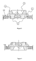
- FIG. 3 shows the invention mounted onto a PCB sub-system using side protrusions as a means for electrical connection.
- FIG. 4 shows the invention mounted onto a PCB sub-system, similar to FIG. 3 , but on a reverse orientation so as to provide bottom illumination.
- the present invention relates to a surface mount optoelectronic component.
- the optoelectronic component is based on surface mount technology.
- a thick, electrically conductive material ( 1 ), preferably a metal frame, is used to serve as a base material for the assembly.
- An opaque plastic material ( 2 ) is used to provide the housing for the whole component.
- a cavity ( 5 ) is designed within the plastic material.
- An optoelectronic chip ( 3 ) is mounted within this cavity. This cavity is filled with a hard transparent or translucent resin material so that optical radiation may be transmitted or received via this window. Electrical connection(s) between the optoelectronic chip ( 3 ) and the base material ( 1 ) is/are provided by a metallic wire ( 4 ).
- the base material ( 1 ) itself, typically by soldering. No extra mechanical forming processes are necessary to create the external connections.
- the base material ( 1 ) extends all the way from a middle portion of the optoelectronic component to a bottom surface ( 8 ), and to one of the side surfaces ( 7 ), ultimately extending and protruding outside the plastic package.
- the bottom surface ( 8 ) is used for connection when a top illuminator is required.
- one of the side surfaces ( 7 ) could be used for connection when the optoelectronic component is used as a side illuminator.
- the base material can also protrude to other side surfaces of the optoelectronic component, with protrusions ( 6 ) formed in the side surface of the package. These protrusions ( 6 ) act as heat sinks to improve heat dissipation from the optoelectronic component.
- the side protrusions ( 6 ) can also be used as a means of connection to external surfaces, such as PCBs, as illustrated in FIGS. 3 and 4 .
- the component sits in the sub-system and can be used for either top or bottom illumination.
- This mounting configuration reduces the height profile of the optoelectronic component above the sub-system, since a portion of the optoelectronic component is below the sub-system's surface.
- the other two exposed surfaces ( 7 ) and ( 8 ) act as heat sinks when used in such mounting configuration.
- Another inherent feature of this invention is the relatively thicker base material compared to other corresponding products in the market. This, coupled with the heat sinks, greatly improves the package's ability to dissipate heat. Higher current or power can also be applied to the devices to yield better performance.
Landscapes
- Engineering & Computer Science (AREA)
- Microelectronics & Electronic Packaging (AREA)
- Structures Or Materials For Encapsulating Or Coating Semiconductor Devices Or Solid State Devices (AREA)
- Led Device Packages (AREA)
Abstract
Description
Claims (20)
Priority Applications (1)
| Application Number | Priority Date | Filing Date | Title |
|---|---|---|---|
| US10/766,468 US7696526B2 (en) | 2004-01-29 | 2004-01-29 | Surface mount optoelectronic component |
Applications Claiming Priority (1)
| Application Number | Priority Date | Filing Date | Title |
|---|---|---|---|
| US10/766,468 US7696526B2 (en) | 2004-01-29 | 2004-01-29 | Surface mount optoelectronic component |
Publications (2)
| Publication Number | Publication Date |
|---|---|
| US20050168922A1 US20050168922A1 (en) | 2005-08-04 |
| US7696526B2 true US7696526B2 (en) | 2010-04-13 |
Family
ID=34807585
Family Applications (1)
| Application Number | Title | Priority Date | Filing Date |
|---|---|---|---|
| US10/766,468 Expired - Lifetime US7696526B2 (en) | 2004-01-29 | 2004-01-29 | Surface mount optoelectronic component |
Country Status (1)
| Country | Link |
|---|---|
| US (1) | US7696526B2 (en) |
Cited By (9)
| Publication number | Priority date | Publication date | Assignee | Title |
|---|---|---|---|---|
| USD627311S1 (en) * | 2010-02-01 | 2010-11-16 | Foxsemicon Integrated Technology, Inc. | Light-emitting diode |
| USD627313S1 (en) * | 2010-02-01 | 2010-11-16 | Foxsemicon Integrated Technology, Inc. | Light-emitting diode |
| USD627312S1 (en) * | 2010-02-01 | 2010-11-16 | Foxsemicon Integrated Technology, Inc. | Light-emitting diode |
| USD627314S1 (en) * | 2010-02-01 | 2010-11-16 | Foxsemicon Integrated Technology, Inc. | Light-emitting diode |
| USD647069S1 (en) * | 2010-05-07 | 2011-10-18 | Nichia Corporation | Light emitting diode |
| USD651183S1 (en) * | 2010-02-01 | 2011-12-27 | Foxsemicon Integrated Technology, Inc. | Light-emitting diode |
| USD651184S1 (en) * | 2009-10-26 | 2011-12-27 | Foxsemicon Integrated Technology, Inc | Light emitting diode |
| USD654443S1 (en) * | 2009-10-26 | 2012-02-21 | Foxsemicon Integrated Technology, Inc. | Light emitting diode |
| US8134173B2 (en) * | 2008-12-25 | 2012-03-13 | Seiko Instruments Inc. | Lighting device having light emitting element mounted in glass substrate |
Families Citing this family (5)
| Publication number | Priority date | Publication date | Assignee | Title |
|---|---|---|---|---|
| WO2007058514A1 (en) | 2005-11-21 | 2007-05-24 | Seoul Semiconductor Co., Ltd. | Light emitting element |
| JP4689637B2 (en) * | 2007-03-23 | 2011-05-25 | シャープ株式会社 | Semiconductor light emitting device |
| US8710538B2 (en) * | 2011-10-05 | 2014-04-29 | Avago Technologies General Ip (Singapore) Pte. Ltd. | Light-emitting device with a spacer at bottom surface |
| EP3138734B1 (en) | 2015-09-03 | 2020-04-15 | SMR Patents S.à.r.l. | Light module, light assembly and rear view device for a vehicle |
| US10403792B2 (en) | 2016-03-07 | 2019-09-03 | Rayvio Corporation | Package for ultraviolet emitting devices |
Citations (11)
| Publication number | Priority date | Publication date | Assignee | Title |
|---|---|---|---|---|
| JPH0685325A (en) * | 1992-08-28 | 1994-03-25 | Stanley Electric Co Ltd | LED manufacturing method |
| JPH06204568A (en) * | 1992-12-30 | 1994-07-22 | Stanley Electric Co Ltd | Lead frame terminal structure |
| USD432095S (en) * | 1998-10-09 | 2000-10-17 | Vishay Semiconductor Gmbh | Light-emitting semi-conductor component |
| US6335548B1 (en) * | 1999-03-15 | 2002-01-01 | Gentex Corporation | Semiconductor radiation emitter package |
| US6355946B1 (en) * | 1998-12-16 | 2002-03-12 | Rohm Co., Ltd. | Semiconductor device with reflector |
| US20020121683A1 (en) * | 2001-02-27 | 2002-09-05 | Kelly Stephen G. | Encapsulated die package with improved parasitic and thermal performance |
| US20020163001A1 (en) * | 2001-05-04 | 2002-11-07 | Shaddock David Mulford | Surface mount light emitting device package and fabrication method |
| US6483623B1 (en) * | 1997-11-28 | 2002-11-19 | Dowa Mining Co., Ltd. | Lamp apparatus for use in optical communication and a process for producing the same |
| US6624491B2 (en) * | 1998-06-30 | 2003-09-23 | Osram Opto Semiconductors Gmbh & Co. | Diode housing |
| US20040000727A1 (en) * | 2002-06-26 | 2004-01-01 | Lingsen Precision Industries, Ltd. | LED package and the process making the same |
| USD505396S1 (en) * | 2003-03-03 | 2005-05-24 | Nichia Corporation | Light emitting diode |
-
2004
- 2004-01-29 US US10/766,468 patent/US7696526B2/en not_active Expired - Lifetime
Patent Citations (11)
| Publication number | Priority date | Publication date | Assignee | Title |
|---|---|---|---|---|
| JPH0685325A (en) * | 1992-08-28 | 1994-03-25 | Stanley Electric Co Ltd | LED manufacturing method |
| JPH06204568A (en) * | 1992-12-30 | 1994-07-22 | Stanley Electric Co Ltd | Lead frame terminal structure |
| US6483623B1 (en) * | 1997-11-28 | 2002-11-19 | Dowa Mining Co., Ltd. | Lamp apparatus for use in optical communication and a process for producing the same |
| US6624491B2 (en) * | 1998-06-30 | 2003-09-23 | Osram Opto Semiconductors Gmbh & Co. | Diode housing |
| USD432095S (en) * | 1998-10-09 | 2000-10-17 | Vishay Semiconductor Gmbh | Light-emitting semi-conductor component |
| US6355946B1 (en) * | 1998-12-16 | 2002-03-12 | Rohm Co., Ltd. | Semiconductor device with reflector |
| US6335548B1 (en) * | 1999-03-15 | 2002-01-01 | Gentex Corporation | Semiconductor radiation emitter package |
| US20020121683A1 (en) * | 2001-02-27 | 2002-09-05 | Kelly Stephen G. | Encapsulated die package with improved parasitic and thermal performance |
| US20020163001A1 (en) * | 2001-05-04 | 2002-11-07 | Shaddock David Mulford | Surface mount light emitting device package and fabrication method |
| US20040000727A1 (en) * | 2002-06-26 | 2004-01-01 | Lingsen Precision Industries, Ltd. | LED package and the process making the same |
| USD505396S1 (en) * | 2003-03-03 | 2005-05-24 | Nichia Corporation | Light emitting diode |
Cited By (9)
| Publication number | Priority date | Publication date | Assignee | Title |
|---|---|---|---|---|
| US8134173B2 (en) * | 2008-12-25 | 2012-03-13 | Seiko Instruments Inc. | Lighting device having light emitting element mounted in glass substrate |
| USD651184S1 (en) * | 2009-10-26 | 2011-12-27 | Foxsemicon Integrated Technology, Inc | Light emitting diode |
| USD654443S1 (en) * | 2009-10-26 | 2012-02-21 | Foxsemicon Integrated Technology, Inc. | Light emitting diode |
| USD627311S1 (en) * | 2010-02-01 | 2010-11-16 | Foxsemicon Integrated Technology, Inc. | Light-emitting diode |
| USD627313S1 (en) * | 2010-02-01 | 2010-11-16 | Foxsemicon Integrated Technology, Inc. | Light-emitting diode |
| USD627312S1 (en) * | 2010-02-01 | 2010-11-16 | Foxsemicon Integrated Technology, Inc. | Light-emitting diode |
| USD627314S1 (en) * | 2010-02-01 | 2010-11-16 | Foxsemicon Integrated Technology, Inc. | Light-emitting diode |
| USD651183S1 (en) * | 2010-02-01 | 2011-12-27 | Foxsemicon Integrated Technology, Inc. | Light-emitting diode |
| USD647069S1 (en) * | 2010-05-07 | 2011-10-18 | Nichia Corporation | Light emitting diode |
Also Published As
| Publication number | Publication date |
|---|---|
| US20050168922A1 (en) | 2005-08-04 |
Similar Documents
| Publication | Publication Date | Title |
|---|---|---|
| US12007081B2 (en) | Lighting assembly and method for manufacturing a lighting assembly | |
| US7696526B2 (en) | Surface mount optoelectronic component | |
| CA2342267C (en) | Led integrated heat sink | |
| US7264378B2 (en) | Power surface mount light emitting die package | |
| US7528414B2 (en) | Light emitting diode package structure | |
| CN100452380C (en) | Surface mount semiconductor device and its lead frame structure | |
| US7963674B2 (en) | Light emitting diode package having flexible PCT directly connected to light source | |
| US20080283861A1 (en) | Power light emitting die package with reflecting lens and the method of making the same | |
| US20070290328A1 (en) | Light emitting diode module | |
| US20070290307A1 (en) | Light emitting diode module | |
| US20100270565A1 (en) | Semiconductor light-emitting device and method of fabricating the same | |
| JP2005294736A (en) | Manufacturing method of semiconductor light emitting device | |
| JP2008502160A (en) | Power light emitting die package having a reflective lens and method of manufacturing | |
| JP3770192B2 (en) | Chip-type LED lead frame | |
| JP2007049152A (en) | LED package and manufacturing method thereof | |
| US11435038B2 (en) | Lighting assembly and method for manufacturing a lighting assembly | |
| KR20060068371A (en) | High power light emitting diode package and its manufacturing method | |
| JP2005116937A (en) | Semiconductor light emitting device and manufacturing method thereof | |
| JP5556369B2 (en) | LIGHT EMITTING DEVICE AND DISPLAY DEVICE USING THE SAME | |
| US20050009242A1 (en) | Packaging method for thin integrated circuits | |
| KR20140145412A (en) | Lighting source module and light system having the same | |
| JPS62106488A (en) | Display unit using light emitting diode | |
| CN100502068C (en) | Packaging structure of light emitting diode | |
| JP2010040563A (en) | Led lighting structure, and manufacturing method thereof | |
| MY164586A (en) | A miniaturised surface mount optoelectronic component |
Legal Events
| Date | Code | Title | Description |
|---|---|---|---|
| AS | Assignment |
Owner name: DOMINANT OPTO TECHNOLOGIES SDN BHD,MALAYSIA Free format text: ASSIGNMENT OF ASSIGNORS INTEREST;ASSIGNORS:TAY, KHENG CHIONG;LAI, KHIN SHIN;LOW, TEK BENG;REEL/FRAME:024064/0815 Effective date: 20100303 |
|
| STCF | Information on status: patent grant |
Free format text: PATENTED CASE |
|
| CC | Certificate of correction | ||
| FPAY | Fee payment |
Year of fee payment: 4 |
|
| MAFP | Maintenance fee payment |
Free format text: PAYMENT OF MAINTENANCE FEE, 8TH YEAR, LARGE ENTITY (ORIGINAL EVENT CODE: M1552) Year of fee payment: 8 |
|
| MAFP | Maintenance fee payment |
Free format text: PAYMENT OF MAINTENANCE FEE, 12TH YEAR, LARGE ENTITY (ORIGINAL EVENT CODE: M1553); ENTITY STATUS OF PATENT OWNER: LARGE ENTITY Year of fee payment: 12 |