US7696021B2 - Semiconductor device manufactured using a non-contact implant metrology - Google Patents
Semiconductor device manufactured using a non-contact implant metrology Download PDFInfo
- Publication number
- US7696021B2 US7696021B2 US11/559,271 US55927106A US7696021B2 US 7696021 B2 US7696021 B2 US 7696021B2 US 55927106 A US55927106 A US 55927106A US 7696021 B2 US7696021 B2 US 7696021B2
- Authority
- US
- United States
- Prior art keywords
- dielectric layer
- implant process
- dopant
- ion implant
- electrical characteristic
- Prior art date
- Legal status (The legal status is an assumption and is not a legal conclusion. Google has not performed a legal analysis and makes no representation as to the accuracy of the status listed.)
- Active, expires
Links
Images


Classifications
-
- H—ELECTRICITY
- H01—ELECTRIC ELEMENTS
- H01L—SEMICONDUCTOR DEVICES NOT COVERED BY CLASS H10
- H01L21/00—Processes or apparatus adapted for the manufacture or treatment of semiconductor or solid state devices or of parts thereof
- H01L21/02—Manufacture or treatment of semiconductor devices or of parts thereof
- H01L21/04—Manufacture or treatment of semiconductor devices or of parts thereof the devices having at least one potential-jump barrier or surface barrier, e.g. PN junction, depletion layer or carrier concentration layer
- H01L21/18—Manufacture or treatment of semiconductor devices or of parts thereof the devices having at least one potential-jump barrier or surface barrier, e.g. PN junction, depletion layer or carrier concentration layer the devices having semiconductor bodies comprising elements of Group IV of the Periodic System or AIIIBV compounds with or without impurities, e.g. doping materials
- H01L21/26—Bombardment with radiation
- H01L21/263—Bombardment with radiation with high-energy radiation
- H01L21/265—Bombardment with radiation with high-energy radiation producing ion implantation
- H01L21/26506—Bombardment with radiation with high-energy radiation producing ion implantation in group IV semiconductors
- H01L21/26513—Bombardment with radiation with high-energy radiation producing ion implantation in group IV semiconductors of electrically active species
-
- H—ELECTRICITY
- H01—ELECTRIC ELEMENTS
- H01L—SEMICONDUCTOR DEVICES NOT COVERED BY CLASS H10
- H01L21/00—Processes or apparatus adapted for the manufacture or treatment of semiconductor or solid state devices or of parts thereof
- H01L21/02—Manufacture or treatment of semiconductor devices or of parts thereof
- H01L21/04—Manufacture or treatment of semiconductor devices or of parts thereof the devices having at least one potential-jump barrier or surface barrier, e.g. PN junction, depletion layer or carrier concentration layer
- H01L21/18—Manufacture or treatment of semiconductor devices or of parts thereof the devices having at least one potential-jump barrier or surface barrier, e.g. PN junction, depletion layer or carrier concentration layer the devices having semiconductor bodies comprising elements of Group IV of the Periodic System or AIIIBV compounds with or without impurities, e.g. doping materials
- H01L21/30—Treatment of semiconductor bodies using processes or apparatus not provided for in groups H01L21/20 - H01L21/26
- H01L21/31—Treatment of semiconductor bodies using processes or apparatus not provided for in groups H01L21/20 - H01L21/26 to form insulating layers thereon, e.g. for masking or by using photolithographic techniques; After treatment of these layers; Selection of materials for these layers
- H01L21/3105—After-treatment
- H01L21/3115—Doping the insulating layers
- H01L21/31155—Doping the insulating layers by ion implantation
-
- H—ELECTRICITY
- H01—ELECTRIC ELEMENTS
- H01L—SEMICONDUCTOR DEVICES NOT COVERED BY CLASS H10
- H01L22/00—Testing or measuring during manufacture or treatment; Reliability measurements, i.e. testing of parts without further processing to modify the parts as such; Structural arrangements therefor
- H01L22/10—Measuring as part of the manufacturing process
- H01L22/14—Measuring as part of the manufacturing process for electrical parameters, e.g. resistance, deep-levels, CV, diffusions by electrical means
Definitions
- the invention is directed, in general, to semiconductor device manufacturing and, more specifically, to a non-contact method of characterizing an implant process.
- MOS transistor features As the size of MOS transistor features continues to shrink, some dopants used to fabricate the transistors are implanted at shallower depths. Specifically, so-called “ultra-shallow” junctions are thought to successfully improve device performance with scaling. These junctions generally provide better threshold voltage control, improve transistor performance, reduce CHC (Channel Hot Carrier) degradation and reduce parasitic capacitance.
- CHC Chip Hot Carrier
- an implant process could be characterized by physical contact with a metrology wafer into which the dopant is implanted using the production process.
- the implant energy of a dopant is sufficiently high, and the implant depth sufficiently large, four-point measurement may be used to determine the resistivity of the metrology wafer.
- the depth of the doped region is less than about the spacing between electrodes used for four-point measurement, electric field lines of the four-point probe may extend below the doped layer.
- the measured resistivity may be dominated by the undoped substrate below the doped layer.
- four-point measurement of test doped layers formed by shallow implants may not accurately represent the characteristics of the doped layer.
- sheet resistance measurements become unreliable for manufacturing purposes. This limitation is particularly applicable for shallow implants used in MOS transistor technology associated with a transistor gate length of about 45 nm or less.
- the invention in one aspect, provides a method of manufacturing a semiconductor device.
- the method includes calibrating an ion implant process by forming an oxide layer over a calibration substrate.
- a dopant is implanted into the oxide layer, and charge is deposited on a surface of the oxide layer using a coronal discharge.
- a voltage on the surface of the oxide layer is measured using an oscillating probe, and an electrical characteristic of the oxide layer is determined therefrom.
- the electrical characteristic is associated with an ion implant process operating set-point to calibrate the ion implant process.
- the dopant is implanted into source/drain regions in a semiconductor substrate using the calibrated ion implant process.
- Another embodiment is a method of manufacturing a semiconductor device.
- the method includes calibrating an ion implant process by forming a dielectric layer over a calibration substrate.
- a dopant is implanted into the dielectric layer, and an electrical characteristic of the dielectric layer is determined.
- the electrical characteristic is associated with an ion implant process operating set-point to calibrate the ion implant process.
- the calibrated ion implant process is used to implant the dopant into a semiconductor substrate.
- Another embodiment is a semiconductor device, including a semiconductor substrate and transistors formed thereover.
- the transistors have source/drain regions formed by an implant process calibrated by forming a dielectric layer over a calibration substrate.
- a dopant is implanted into the dielectric layers and charge is deposited on a surface of the dielectric layer using a coronal discharge.
- a voltage on the surface of the dielectric layer is measured, and an electrical characteristic of the dielectric layer is determined therefrom. The electrical characteristic is associated with a concentration of a dopant in the doped regions to calibrate the ion implant process.
- Interconnect layers within dielectric layers over the transistors are configured to connect the transistors.
- FIG. 1 illustrates a MOS transistor
- FIG. 2 illustrates implantation of a dopant
- FIG. 3 illustrates a dielectric layer into which a dopant has been implanted
- FIGS. 4 and 5 illustrate electrical characterization of a doped dielectric layer
- FIGS. 6-8 illustrate of electrical characteristics of a doped oxide layer
- FIG. 9 illustrates an integrated circuit
- the present invention recognizes that a manufacturable non-contact method of determining electrical characteristics of shallow dopant implants may be used to calibrate an implant process to maintain consistent performance of semiconductor devices formed using the implant process.
- the implant process may be calibrated for a desired dopant species by forming a dielectric layer.
- the dopant is implanted into the dielectric layer and creates damage therein.
- a non-contact corona charge deposition technique may be used to characterize electrical properties of the dielectric layer, which are altered by damage caused by the implant process. Changes to the electrical properties can then be used to monitor the implant process.
- FIG. 1 illustrates a MOS transistor 100 .
- the transistor 100 includes a gate structure 110 and sidewall structures 120 .
- Source/drain regions 130 are adjacent the gate structure 110 , and are formed using one or more ion implant processes that place impurity atoms into the source/drain regions 130 to produce desired transistor electrical characteristics.
- the source/drain regions 130 include a portion 140 in which the depth and concentration of dopants in the source/drain regions 130 are varied to reduce certain undesirable effects such as channel hot carrier (CHC) and parasitic capacitance.
- the source/drain regions are typically formed using multiple dopant implants of varying energy and implant angle.
- the source/drain regions 130 may include a lightly doped drain (LDD) or a medium-doped drain (MDD) portion 150 , a source/drain extension (SDE) portion 160 and a source/drain portion 170 .
- LDD/MDD 150 and SDE 160 portions may be significantly shallower than the source/drain portion 170 .
- Unstable electrical performance of the transistors 100 over time is highly undesirable in a manufacturing environment. Improving consistency of the implant process used to form the LDD/MDD 150 and SDE 160 portions may reduce this instability. By monitoring the implant process over time, the consistency of the implant process may be improved.
- the method described herein employs characterization techniques that focus on a thin doped region near the surface of a doped dielectric film.
- electrical thickness, tunneling field, and resistivity may be determined using noncontact methods that provide the desired sensitivity to the portion of the dielectric film containing the implanted dopant. These electrical characteristics may be associated with ion implant process conditions, including dose, energy and implant species, in order to calibrate the implant process.
- FIG. 2 illustrates a calibration substrate 210 on which a dielectric layer 220 has been formed.
- the calibration substrate 210 may be a semiconductor substrate on which a high-quality dielectric layer may be formed.
- the calibration substrate 210 has sufficient conductivity to act as a lower electrode of a parallel-plate capacitor using the dielectric layer 220 as a polarizable medium.
- the calibration substrate 210 is used to calibrate a process and is not used to manufacture semiconductor devices thereon.
- the dielectric layer 220 may be any dielectric material having high initial resistivity and low concentration of defects that may act as charge traps and enable electron mobility.
- the dielectric layer 220 may be a thermally grown oxide of the calibration substrate 210 .
- Other dielectrics may also be used, such as a thermally grown nitride or a dielectric formed by a chemical vapor deposition (CVD) or a physical vapor deposition (PVD) process.
- the calibration substrate 210 is a doped silicon wafer, and the dielectric layer 220 is thermally grown silicon dioxide.
- An ion implant process 230 is used to implant a dopant into the dielectric layer 220 .
- An ion implant process is a process by which impurity atoms, or dopants, are placed into a semiconductor substrate. The dopants are generally ionized and then accelerated by an electric field to a velocity sufficient to penetrate the surface of the substrate. Typically, the depth and distribution of the implanted impurity atoms are determined in part by the implant species, energy of the accelerated ions (expressed in units of keV or MeV), and dose (expressed as atoms/cm 2 of the substrate surface).
- the implant process 230 may be a production ion implant process used to form the LDD/MDD 150 and SDE 160 regions of the MOS transistor 100 .
- Implanted species may include boron (B), arsenic (As), and phosphorous (P), but the method is not so limited.
- B boron
- As arsenic
- P phosphorous
- FIG. 3 illustrates a doped dielectric layer 310 resulting from implanting the dopant into the dielectric layer 220 .
- the ion implantation process 230 results in a distribution 320 of the dopant in the doped dielectric layer 310 .
- the distribution 320 has a peak concentration at a mean depth T and a standard deviation (not shown) about the mean.
- the dopant atoms may break bonds between atoms in the doped dielectric layer 310 , resulting in dangling bonds therein.
- the dopant atoms may also have unfilled atomic orbitals resulting in additional dangling bonds.
- the dangling bonds may result in conduction paths 330 in the dielectric layer 310 which provide a relatively low resistance path from a surface 340 of the doped dielectric layer 310 to the substrate 210 thereunder. Implications of these paths 330 are discussed below.
- the thickness of the dielectric layer 220 is chosen to provide sufficient sensitivity of measured electrical characteristics of the doped dielectric layer 310 . If the dielectric layer 310 is too thin, the dopant and implantation damage therein may result in sufficient conductivity to make measurement of capacitance difficult. Conversely, if the doped dielectric layer 310 is too thick, conductivity may be below detection limits. In general, a desired thickness of the dielectric layer 220 is dependent on the conditions used to implant the dopant. In one embodiment, the dielectric layer 220 is a thermal silicon dioxide layer with a thickness of about 50 nm.
- This thickness provides sufficient sensitivity to characterize a process implanting As with an energy ranging from about 6 keV to about 12 keV, and a dose ranging from about 1E14 atoms/cm 2 to about 1E15 atoms/cm 2 .
- FIG. 4 illustrates the placement of electric charge Q surface on the surface 340 of the doped dielectric layer 310 .
- the substrate 210 with the doped dielectric layer 310 thereon rests on a cathode 410 .
- a corona gun 420 acts as an anode and is energized by a power source 430 to produce an electron flux 440 .
- a corona gun is a source of electrons produced by an electrode raised to a high electrical potential. Electrons may “boil” off the surface of the electrode and travel to the surface 340 . Because the doped dielectric layer 310 is a dielectric material, some electrons impinging on the surface 340 are relatively immobile.
- the surface charge 450 creates a surface potential on the surface 340 and an image charge 460 in the substrate 210 .
- the surface charge 450 and the image charge 460 act as plates of a “virtual” parallel-plate capacitor with the portion of the doped dielectric layer 310 therebetween acting as the polarizable medium of the capacitor.
- FIG. 5 illustrates an electrostatic probe 510 used to measure the electrical potential on the surface 340 produced by the surface charge 450 .
- the electrostatic probe 510 may be a Kelvin probe.
- a Kelvin probe is well known in the art and is therefore only briefly described here.
- a Kelvin probe typically includes a capacitive element (not shown) and a vibrator 520 .
- the capacitive element is positioned proximate a charge layer with a small air gap.
- the vibrator 520 causes the distance between the charge layer and the capacitive element to vary, thus inducing a time-varying electric voltage on the capacitive element.
- the time-varying voltage is converted to a useable signal by a controller 530 , and a value of the surface charge 450 is derived therefrom.
- a tool that provides the described functionality is a QuantoxTM XP in-line electrical monitoring and characterization system manufactured by KLA-Tencor, San Jose, Calif.
- the QuantoxTM system provides an integrated capability to deposit the coronal charge on the surface of the doped dielectric layer 310 and to measure the surface charge 450 using a Kelvin probe.
- the QuantoxTM system mounts a corona gun and a Kelvin probe on a translatable stage that permits measurement of the substrate voltage after deposition of charge on the surface without manipulation of the substrate 210 .
- the QuantoxTM system is compatible with production clean room environments used to fabricate integrated circuits.
- the capacitance of the virtual capacitor may be determined from the value of the surface charge Q surface and the measured potential of the surface charge.
- An electrical thickness of the doped dielectric layer 310 may be determined from the computed capacitance. Electrical thickness as used herein means an equivalent thickness of the doped dielectric layer 310 assuming a material layer with homogeneous resistivity and dielectric permittivity. The electrical thickness may be determined from the equation for a parallel-plate capacitor; namely,
- T Electrical ⁇ o ⁇ A C film ( 2 )
- ⁇ is the relative dielectric permittivity of the dielectric layer 220
- ⁇ o is the permittivity of free space
- A is the area of the capacitor (the Kelvin probe capacitive element)
- C film is the capacitance calculated from EQ. 1. It is apparent from EQ. 2 that the electrical thickness is inversely proportional to C film . As a result, changes of the calculated capacitance result in inversely proportional changes of the electrical thickness.
- the capacitance may be changed when impurity atoms are implanted into the doped dielectric layer 310 . It is thought that the dopant atoms increase the number of polarizable sites in the doped dielectric layer 310 , resulting in an increase of the relative dielectric permittivity of the doped dielectric layer 310 . When the relative permittivity of the doped dielectric layer 310 increases, the capacitance produced by a given charge Q surface also increases. Referring to EQ. 2, the increased capacitance then results in a reduced electrical thickness of the doped dielectric layer 310 .
- the doped portion of the doped dielectric layer 310 may act as a plate of the virtual capacitor, thereby decreasing the distance between the charged regions bordering the undoped portions of the doped dielectric 310 . This lower distance will increase the calculated capacitance of the virtual capacitor, thereby decreasing the computed electrical thickness of the doped dielectric layer 310 .
- the combination of these effects is expected to result in a decrease of the electrical thickness and resistivity of the doped dielectric layer 310 as the doping level and implant energy of the dopant are increased.
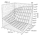
- FIG. 6 illustrates a surface response 610 of the calculated electrical thickness of a silicon dioxide layer as a function of As implant energy and dose.
- the electrical thickness of the silicon dioxide layer decreases smoothly in a monotonic manner as either the implant energy or the dose increases. Desired electrical characteristics of transistors formed using the implant process may advantageously be correlated with a point on the response surface 610 . If desired, multiple implant conditions may be characterized to enable computation of the implant energy and dose corresponding to a calculated electrical thickness.
- a measure of the tunneling field strength is used to characterize the implant process 230 .
- the tunneling field strength of the doped dielectric layer 310 is the maximum potential that may be produced by a corona discharge on the surface 340 .
- the maximum sustainable charge on the surface 340 associated with the maximum potential is a “saturation charge.” It is thought that at the tunneling field strength, current from the corona gun 420 is balanced by current through the doped dielectric layer 310 by quantum tunneling so that a potential strength does not exceed a maximum value, i.e., the tunneling field strength. It is further thought that the current occurs by electron hopping between the defects previously described in the doped dielectric layer 310 produced by the implant process 230 . Thus, more current is able to flow by tunneling effects as additional damage occurs to the doped dielectric layer 310 .
- FIG. 7 illustrates a surface response 710 of the tunneling field strength of a silicon dioxide layer as a function of As implant energy and dose as determined using a QuantoxTM system.
- the tunneling field again decreases monotonically as either the implant energy or dose is increased.
- the well-behaved nature of the response surface 710 provides another means to monitor the implant process 230 .
- desirable electrical characteristics of production transistors may be correlated with the measured tunneling field strength of the dielectric layer 310 .
- a deviation of the tunneling field strength from a calibrated value is a signal that the implant process may have drifted, and appropriate corrective action may be taken to return or adjust process parameters to a setting that appropriately corrects the drift.
- resistivity of the doped dielectric layer 310 is Another electrical characteristic of the doped dielectric layer 310 that may be used to monitor the implant process 230 .
- the resistivity of a material is a measure of how well the material opposes the flow of current, and is typically expressed in SI units of ohm-cm.
- the resistivity p of the doped dielectric layer 310 may be determined from Ohm's law by characterizing the current flow through the doped dielectric layer 310 at a known potential of the surface 340 , with knowledge of the physical thickness of the doped dielectric layer 310 . The resistivity may then be determined by the relationship
- V surface is the potential produced by the surface charge 450
- A is the area of the portion of the dielectric layer 340 characterized
- I is the measured current
- T is the physical thickness of the doped dielectric layer 310 .
- FIG. 8 illustrates a response surface 810 of the calculated resistivity of a silicon dioxide layer determined using a QuantoxTM system.
- the resistivity again decreases monotonically as either the implant energy or dose is increased.
- the response surface 810 provides yet another means to monitor the implant process 230 , using the correlation method described previously.
- the described method provides a manufacturable means of monitoring the implant process 230 used to produce shallow implants in production transistors.
- the electrical thickness, tunneling field and resistivity of the doped dielectric layer 310 each provide a means to monitor the implant process 230 .
- the implant process 230 may be investigated to determine the cause of the deviation and corrective may be taken.
- the method is not so limited.
- the method may also be used with other implant processes, including but not limited to HALO (high-angle, low energy) implants, “pocket” implants, channel implants and formation of doped regions of bipolar junction transistors.
- HALO high-angle, low energy
- the described method may be easily adapted as a metrology method for ion implantation processes.
- the electrical thickness, tunneling field and resistivity characteristics of a doped dielectric layer may be used individually or in combination to determine the implant dose from the implant energy or the implant energy from the implant dose.
- the elements of the method may find broad application in the ion implantation arts.
- FIG. 9 illustrates an integrated circuit (IC) 900 formed using an implant process calibrated by the method described herein.
- Transistors 910 are formed over a substrate 920 , and include source/drain regions 930 .
- the source/drain regions 930 are formed using an implant process that has been calibrated by monitoring an electrical characteristic of a calibration substrate.
- the calibrated implant process may be used to form a shallow implant region 940 such as an MDD or an SDE of the transistors 910 .
- the IC 900 may include MOS, BiCMOS or bipolar components, and may further include passive components, such as capacitors, inductors or resistors. It may also include optical components or optoelectronic components. Those skilled in the art are familiar with these various types of components and their manufacture.
- the IC 900 may also be a dual-voltage IC, comprising transistors operating with difference threshold voltages.
- Dielectric layers 950 may be fabricated over the transistors 910 using currently known or later discovered methods. Additionally, interconnect structures 960 are located within the dielectric layers 950 to connect various components, thus forming the operational integrated circuit 900 . It will be apparent to one skilled in the art that several variations of the example interconnect architecture may be fabricated according to the principles of the invention with similarly advantageous results.
Abstract
Description
provides the relationship between these values.
where κ is the relative dielectric permittivity of the
where Vsurface is the potential produced by the
Claims (15)
Priority Applications (1)
| Application Number | Priority Date | Filing Date | Title |
|---|---|---|---|
| US11/559,271 US7696021B2 (en) | 2005-11-14 | 2006-11-13 | Semiconductor device manufactured using a non-contact implant metrology |
Applications Claiming Priority (2)
| Application Number | Priority Date | Filing Date | Title |
|---|---|---|---|
| US73643505P | 2005-11-14 | 2005-11-14 | |
| US11/559,271 US7696021B2 (en) | 2005-11-14 | 2006-11-13 | Semiconductor device manufactured using a non-contact implant metrology |
Publications (2)
| Publication Number | Publication Date |
|---|---|
| US20080006886A1 US20080006886A1 (en) | 2008-01-10 |
| US7696021B2 true US7696021B2 (en) | 2010-04-13 |
Family
ID=38918379
Family Applications (1)
| Application Number | Title | Priority Date | Filing Date |
|---|---|---|---|
| US11/559,271 Active 2027-04-20 US7696021B2 (en) | 2005-11-14 | 2006-11-13 | Semiconductor device manufactured using a non-contact implant metrology |
Country Status (1)
| Country | Link |
|---|---|
| US (1) | US7696021B2 (en) |
Cited By (1)
| Publication number | Priority date | Publication date | Assignee | Title |
|---|---|---|---|---|
| US20120139739A1 (en) * | 2010-12-03 | 2012-06-07 | Todd Bishop | Monitored Filament Insertion for Resitivity Testing |
Families Citing this family (6)
| Publication number | Priority date | Publication date | Assignee | Title |
|---|---|---|---|---|
| JP2009004493A (en) * | 2007-06-20 | 2009-01-08 | Toshiba Corp | Semiconductor device and its manufacturing method |
| US8853832B2 (en) * | 2009-01-22 | 2014-10-07 | Stmicroelectronics Inc. | Methods and apparatus for reducing coupling in a MOS device |
| FR2941816B1 (en) * | 2009-02-05 | 2011-04-01 | Commissariat Energie Atomique | METHOD OF CHARACTERIZING A METHOD FOR ION IMPLANTATION |
| EP2757579B1 (en) * | 2013-01-17 | 2019-06-19 | IMEC vzw | Method for characterisation of shallow junctions for use in semiconductor devices |
| KR20150122341A (en) * | 2014-04-23 | 2015-11-02 | 삼성전자주식회사 | Back light apparatus and 3d display apparatus including the same |
| FR3028957B1 (en) * | 2014-11-24 | 2017-09-29 | Commissariat Energie Atomique | METHOD FOR MEASURING THE RESISTANCE OF A COVERED CONDUCTIVE LAYER |
Citations (3)
| Publication number | Priority date | Publication date | Assignee | Title |
|---|---|---|---|---|
| US20030040130A1 (en) * | 2001-08-09 | 2003-02-27 | Mayur Abhilash J. | Method for selection of parameters for implant anneal of patterned semiconductor substrates and specification of a laser system |
| US20040166612A1 (en) * | 2002-06-05 | 2004-08-26 | Applied Materials, Inc. | Fabrication of silicon-on-insulator structure using plasma immersion ion implantation |
| US7403023B2 (en) * | 2005-03-14 | 2008-07-22 | Qc Solutions, Inc. | Apparatus and method of measuring defects in an ion implanted wafer by heating the wafer to a treatment temperature and time to substantially stabilize interstitial defect migration while leaving the vacancy defects substantially unaltered. |
-
2006
- 2006-11-13 US US11/559,271 patent/US7696021B2/en active Active
Patent Citations (3)
| Publication number | Priority date | Publication date | Assignee | Title |
|---|---|---|---|---|
| US20030040130A1 (en) * | 2001-08-09 | 2003-02-27 | Mayur Abhilash J. | Method for selection of parameters for implant anneal of patterned semiconductor substrates and specification of a laser system |
| US20040166612A1 (en) * | 2002-06-05 | 2004-08-26 | Applied Materials, Inc. | Fabrication of silicon-on-insulator structure using plasma immersion ion implantation |
| US7403023B2 (en) * | 2005-03-14 | 2008-07-22 | Qc Solutions, Inc. | Apparatus and method of measuring defects in an ion implanted wafer by heating the wafer to a treatment temperature and time to substantially stabilize interstitial defect migration while leaving the vacancy defects substantially unaltered. |
Cited By (2)
| Publication number | Priority date | Publication date | Assignee | Title |
|---|---|---|---|---|
| US20120139739A1 (en) * | 2010-12-03 | 2012-06-07 | Todd Bishop | Monitored Filament Insertion for Resitivity Testing |
| US9297795B2 (en) * | 2010-12-03 | 2016-03-29 | Todd Nicholas Bishop | Monitored filament insertion for resitivity testing |
Also Published As
| Publication number | Publication date |
|---|---|
| US20080006886A1 (en) | 2008-01-10 |
Similar Documents
| Publication | Publication Date | Title |
|---|---|---|
| US7696021B2 (en) | Semiconductor device manufactured using a non-contact implant metrology | |
| Peiner et al. | Doping profile analysis in Si by electrochemical capacitance‐voltage measurements | |
| US9299622B2 (en) | On-chip plasma charging sensor | |
| US5393691A (en) | Fabrication of w-polycide-to-poly capacitors with high linearity | |
| JP2014146789A (en) | Method for adjusting effective work function of gate structure in semiconductor device | |
| US11610880B2 (en) | Power MOS device having an integrated current sensor and manufacturing process thereof | |
| US6734493B2 (en) | Lateral double diffused metal oxide semiconductor (LDMOS) device with aligned buried layer isolation layer | |
| TW201314811A (en) | Resistive test structure, semiconductor device, and method performed using a resistive device | |
| US7071044B1 (en) | Method of making a test structure for gate-body current and direct extraction of physical gate length using conventional CMOS | |
| US7132683B1 (en) | Dual purpose test structure for gate-body current measurement in PD/SOI and for direct extraction of physical gate length in scaled CMOS technologies | |
| US6486692B1 (en) | Method of positive mobile iron contamination (PMIC) detection and apparatus of performing the same | |
| US6754553B2 (en) | Implant monitoring using multiple implanting and annealing steps | |
| US6709943B2 (en) | Method of forming semiconductor diffused resistors with optimized temperature dependence | |
| De Wolf et al. | Comparison of two-dimensional carrier profiles in metal–oxide–semiconductor field-effect transistor structures obtained with scanning spreading resistance microscopy and inverse modeling | |
| TWI601213B (en) | Methods for characterisation of shallow junctions for use in semiconductor devices | |
| TWI288482B (en) | Transistor Vth auto feedback by local implant | |
| US6822430B2 (en) | Method of assessing lateral dopant and/or charge carrier profiles | |
| EP1610373A2 (en) | Method and apparatus for determining generation lifetime of product semiconductor wafers | |
| US9082660B2 (en) | Method of controlling threshold voltage and method of fabricating semiconductor device | |
| US20220238516A1 (en) | Polysilicon resistor using reduced grain size polysilicon | |
| Liu et al. | Investigation of Indium activation by CV measurement | |
| US6071749A (en) | Process for forming a semiconductor device with controlled relative thicknesses of the active region and gate electrode | |
| TWI250599B (en) | Monitor wafer for high current ion implanter, and the method for monitoring charging using the same | |
| Latif | Characterisation of Sheet Resistivity and Contact Resistivity for Source/Drain of n-MOSFET Device | |
| JP2000021803A (en) | Method of measuring impurity quantity and manufacture of semiconductor device using the method |
Legal Events
| Date | Code | Title | Description |
|---|---|---|---|
| AS | Assignment |
Owner name: TEXAS INSTRUMENTS INCORPORATED,TEXAS Free format text: ASSIGNMENT OF ASSIGNORS INTEREST;ASSIGNORS:MEHTA, NARENDRA SINGH;VARGHESE, AJITH;SIGNING DATES FROM 20061213 TO 20061214;REEL/FRAME:020058/0578 Owner name: TEXAS INSTRUMENTS INCORPORATED, TEXAS Free format text: ASSIGNMENT OF ASSIGNORS INTEREST;ASSIGNORS:MEHTA, NARENDRA SINGH;VARGHESE, AJITH;REEL/FRAME:020058/0578;SIGNING DATES FROM 20061213 TO 20061214 |
|
| STCF | Information on status: patent grant |
Free format text: PATENTED CASE |
|
| FPAY | Fee payment |
Year of fee payment: 4 |
|
| MAFP | Maintenance fee payment |
Free format text: PAYMENT OF MAINTENANCE FEE, 8TH YEAR, LARGE ENTITY (ORIGINAL EVENT CODE: M1552) Year of fee payment: 8 |
|
| MAFP | Maintenance fee payment |
Free format text: PAYMENT OF MAINTENANCE FEE, 12TH YEAR, LARGE ENTITY (ORIGINAL EVENT CODE: M1553); ENTITY STATUS OF PATENT OWNER: LARGE ENTITY Year of fee payment: 12 |