US7673196B2 - Methods and apparatus for communicating with a target circuit - Google Patents
Methods and apparatus for communicating with a target circuit Download PDFInfo
- Publication number
- US7673196B2 US7673196B2 US11/691,838 US69183807A US7673196B2 US 7673196 B2 US7673196 B2 US 7673196B2 US 69183807 A US69183807 A US 69183807A US 7673196 B2 US7673196 B2 US 7673196B2
- Authority
- US
- United States
- Prior art keywords
- data
- vector
- circuit
- memory array
- stored test
- Prior art date
- Legal status (The legal status is an assumption and is not a legal conclusion. Google has not performed a legal analysis and makes no representation as to the accuracy of the status listed.)
- Expired - Fee Related, expires
Links
Images


Classifications
-
- G—PHYSICS
- G01—MEASURING; TESTING
- G01R—MEASURING ELECTRIC VARIABLES; MEASURING MAGNETIC VARIABLES
- G01R31/00—Arrangements for testing electric properties; Arrangements for locating electric faults; Arrangements for electrical testing characterised by what is being tested not provided for elsewhere
- G01R31/28—Testing of electronic circuits, e.g. by signal tracer
- G01R31/317—Testing of digital circuits
- G01R31/3181—Functional testing
- G01R31/3185—Reconfiguring for testing, e.g. LSSD, partitioning
- G01R31/318533—Reconfiguring for testing, e.g. LSSD, partitioning using scanning techniques, e.g. LSSD, Boundary Scan, JTAG
- G01R31/318577—AC testing, e.g. current testing, burn-in
-
- G—PHYSICS
- G11—INFORMATION STORAGE
- G11C—STATIC STORES
- G11C29/00—Checking stores for correct operation ; Subsequent repair; Testing stores during standby or offline operation
- G11C29/04—Detection or location of defective memory elements, e.g. cell constructio details, timing of test signals
- G11C29/08—Functional testing, e.g. testing during refresh, power-on self testing [POST] or distributed testing
- G11C29/12—Built-in arrangements for testing, e.g. built-in self testing [BIST] or interconnection details
- G11C29/14—Implementation of control logic, e.g. test mode decoders
-
- G—PHYSICS
- G11—INFORMATION STORAGE
- G11C—STATIC STORES
- G11C29/00—Checking stores for correct operation ; Subsequent repair; Testing stores during standby or offline operation
- G11C29/04—Detection or location of defective memory elements, e.g. cell constructio details, timing of test signals
- G11C29/08—Functional testing, e.g. testing during refresh, power-on self testing [POST] or distributed testing
- G11C29/12—Built-in arrangements for testing, e.g. built-in self testing [BIST] or interconnection details
- G11C29/18—Address generation devices; Devices for accessing memories, e.g. details of addressing circuits
- G11C29/20—Address generation devices; Devices for accessing memories, e.g. details of addressing circuits using counters or linear-feedback shift registers [LFSR]
-
- G—PHYSICS
- G11—INFORMATION STORAGE
- G11C—STATIC STORES
- G11C29/00—Checking stores for correct operation ; Subsequent repair; Testing stores during standby or offline operation
- G11C29/04—Detection or location of defective memory elements, e.g. cell constructio details, timing of test signals
- G11C29/08—Functional testing, e.g. testing during refresh, power-on self testing [POST] or distributed testing
- G11C29/12—Built-in arrangements for testing, e.g. built-in self testing [BIST] or interconnection details
- G11C29/36—Data generation devices, e.g. data inverters
-
- G—PHYSICS
- G01—MEASURING; TESTING
- G01R—MEASURING ELECTRIC VARIABLES; MEASURING MAGNETIC VARIABLES
- G01R31/00—Arrangements for testing electric properties; Arrangements for locating electric faults; Arrangements for electrical testing characterised by what is being tested not provided for elsewhere
- G01R31/28—Testing of electronic circuits, e.g. by signal tracer
- G01R31/317—Testing of digital circuits
- G01R31/3181—Functional testing
- G01R31/3185—Reconfiguring for testing, e.g. LSSD, partitioning
- G01R31/318533—Reconfiguring for testing, e.g. LSSD, partitioning using scanning techniques, e.g. LSSD, Boundary Scan, JTAG
- G01R31/318544—Scanning methods, algorithms and patterns
- G01R31/318547—Data generators or compressors
Definitions
- the present invention relates to systems and methods for AC testing of a memory array.
- testing a target circuit such as an integrated circuit (IC)
- IC integrated circuit
- prior to packaging may reveal problems associated with the individual ICs and also with the IC fabrication process preceding the packaging step.
- Testing an IC after packaging may reveal problems arising from the packaging process steps, such as die attachment, wire bonding, among other steps.
- So-called scan chain testing techniques may be employed for testing IC circuits before and/or after packaging.
- Existing scan chain test operations for DC testing include scanning a known sequence of bits into a series of respective latches (flip flops) within the IC circuit.
- the latches are selected to direct the scanned bits to the input(s) of the target circuit, such as combinational logic, Static Random Access Memory (SRAM), etc.
- the target circuit is provided with a significant amount of time to let the input sequence of bits settle at the input(s) and outputs of the gates, memory cells, etc., such that test output bits are produced in response to the input bits. In other words, no dynamic testing is conducted.
- the output bits are directed to a selected series of output latches of the IC. Commands are then issued to scan the test output bits from the output latches, and the output bits are compared to a known template to determine whether the target circuit is operational.
- the input latches and output latches are typically already part of the IC and, under normal operating modes, perform functions that permit the IC to operate.
- the testing designer selects the input and output latches from among the latches of the IC to be used in the scan chain testing process.
- Selector circuits may be employed to switch the input/output connections of the selected latches between normal operating modes and the scan chain testing mode. Since the DC scan chain testing process does not perform dynamic (AC) testing, virtually any of the existing latches of the IC may be selected as input/output latches for the scan chain test process no matter where (how far) they may be located relative to the inputs/output of the target circuit, the impedances of the interconnections, or potential sources of electromagnetic interference.
- AC testing techniques typically use a CPU (Central Processing Unit) external to the target circuit to drive data into and out of selected input/output latches adjacent to the target circuit.
- CPU Central Processing Unit
- the CPU is coupled to respective input and output connections for a portion of a circuit being tested which are generally within a limited, localized region of the test circuit.
- it is cumbersome and complex to connect an external CPU in this manner to all portions of a circuit for which testing is sought.
- An ABIST circuit can include an ABIST engine, an array macro, which in turn includes a memory array, and communication links between the ABIST engine and the array macro.
- an array macro may correspond to a circuit that includes a memory array (which may also be referred to as a “memory core”) and additional functionality to enable communication between the memory core and devices external to the array macro.
- a memory array which may also be referred to as a “memory core”
- additional functionality to enable communication between the memory core and devices external to the array macro.
- the ABIST engine For DC testing, the ABIST engine generates “write data” (for storage in the array) and address values and sends both to scannable latches in the array macro. Thereafter, the storage data are stored in the specified addresses in a memory array within the array macro. The ABIST engine then issues a read instruction to the array macro, retrieves output data from the array macro, and compares the retrieved data to expectation data generated by the ABIST engine. The functionality of the array macro is then determined by comparing the expectation data (which generally corresponds to the original write data) with the data retrieved from the array macro.
- the speed at which data can be provided to the memory array is limited by the rate at which the write data and address values can be transmitted from the ABIST engine to the scannable latches of the array macro.
- a few cycles of continuous data transmission to the memory array may be obtained by using multiple sets of (such as two or three) input latches for inputting data to a single set of memory array input lines.
- sending only two or three sets of input “write data” in rapid succession, for AC testing purposes does not sufficiently exercise the various features of the array macro for circuit evaluation purposes.
- the invention is directed to a method that may include establishing a stored test vector, including a plurality of data bits, within a vector data engine; transmitting the stored test vector to a memory array; performing at least one arithmetic or logical operation upon the stored test vector by a vector data generator within the vector data engine to update the stored test vector; and repeating the steps of transmitting and performing so as to continuously transmit continuously changing stored test vectors to the memory array.
- the invention is directed to an apparatus for providing data to memory array that may include a vector data engine having a data storage device and a vector data generator, the vector data engine operable to: establish a stored test vector, including a plurality of data bits, within the data storage device; transmit the stored test vector to the memory array; perform at least one arithmetic or logical operation upon the stored test vector by the vector data generator to update the stored test vector; and continue to transmit and update the stored test vector.
- a vector data engine having a data storage device and a vector data generator, the vector data engine operable to: establish a stored test vector, including a plurality of data bits, within the data storage device; transmit the stored test vector to the memory array; perform at least one arithmetic or logical operation upon the stored test vector by the vector data generator to update the stored test vector; and continue to transmit and update the stored test vector.
- the invention is directed to an apparatus, that may include a memory array; a decoder circuit having a plurality of output pins in communication with the memory array, wherein one and only one of the output pins has an active memory access signal thereon at a time; and a shift counter in communication with the output pins and operable to shift the active signal between successive ones of the output pins.
- FIG. 1 is block diagram of an array macro in communication with an ABIST engine that is adaptable for use with one or more embodiments of the present invention
- FIG. 2 is a block diagram of a circuit for providing vector data to a memory array in accordance with one or more embodiments of the present invention
- FIG. 3 is a block diagram of a circuit for providing address vectors to a memory array in accordance with one or more embodiments of the present invention
- FIG. 4 is schematic diagram of a circuit suitable for implementing one portion of the circuit of FIG. 3 , in accordance with one or more embodiments of the present invention
- FIG. 5 is a schematic diagram of a circuit suitable for implementing one portion of the circuit of FIG. 3 , in accordance with one or more embodiments of the present invention
- FIG. 6 is a timing chart showing the interaction of various signals associated with the operation of the circuits of FIGS. 4 and 5 , in accordance with one or more embodiments of the present invention
- FIG. 7 is a block diagram of a circuit for expediting the provision of a carry signal to a data latch, in accordance with one or more embodiments of the present invention.
- FIG. 8 is a block diagram of a circuit for expediting the provision of a carry signal to a data latch, in accordance with one or more alternative embodiments of the present invention.
- FIG. 9 is a block diagram of a circuit for shifting a signal through a succession of signal paths in accordance with one or more of the embodiments of the present invention.
- FIG. 10 is a flow diagram illustrating process steps that may be carried out in accordance with one or more of the embodiments disclosed and/or discussed herein.
- DC testing generally corresponds to circuit testing which tests the steady state response of a target circuit, or simply “target.”
- the target may be initially in a stable condition, then receive test input data, and then generate test output data, based on logical operations and/or on memory location accesses, by the target.
- the target is generally permitted to reach a steady-state condition and to then allow test output data to be extracted therefrom.
- the target circuit is provided with a significant amount of time to let the input sequence of bits settle at the input(s) and outputs of the gates, memory cells, etc., such that test output bits are produced in response to the input bits. In other words, no dynamic testing is conducted.
- AC testing generally corresponds to circuit testing in which the dynamic response of a target is tested.
- the target may initially be in a stable condition. Thereafter, one or more streams of data bits may be transmitted to the target at a relatively rapid rate, generally corresponding to the conditions the target would experience during normal operation thereof within an integrated circuit.
- the target is generally not given extra time to guarantee that all regions of the target stabilize before sending additional data and/or scanning output data from the target.
- the input bits to the target circuit must be rapidly provided in order to exercise the target circuit in ways that may uncover defects, such as input/output set up times, propagation delays, impedance characteristics, electromagnetic interference sources, etc.
- the real-time, dynamic characteristics of the target such as race conditions, etc., among other characteristics, may be evaluated when employing AC testing techniques.
- FIG. 1 is block diagram of a circuit 100 , including an array macro 120 , in communication with an ABIST engine 110 , that is operable for use with one or more embodiments of the present invention.
- Array macro 120 may include write circuit 132 , read circuit 134 , addressing circuit 140 , row decoder 142 , column decoder 142 , and memory array 150 .
- circuit 100 may write data to memory array 150 , read data out of memory array 150 , and compare the read data to expected values for the read data and establish a pass or fail condition for the test.
- ABIST engine 110 may be a general or special purpose processor that may be operable to generate vector data (“write data”) and/or address vectors (address values) for writing and/or reading data to/from array macro 120 .
- ABIST engine 120 may also be operable to transmit one or more control signals to array macro 120 for controlling writing data thereto, reading data therefrom, and/or testing data therein.
- write circuit 132 may include one or more scannable latches and may be operable to receive data from ABIST engine 110 and re-transmit this data to memory array 150 .
- write circuit 132 may be commanded to write given data to memory array 150 without receiving the given data from ABIST engine 110 .
- the data may result from a “preset condition” activated by suitable control signal(s).
- the given data may be generated by write circuit 132 .
- read circuit 134 may also include one or more scannable latches and may be operable to receive data from memory array 150 and re-transmit this data to ABIST engine 110 .
- addressing circuit 140 may receive address data from ABIST engine 110 . Addressing circuit 140 may also generate address data, as is discussed in greater detail later in this disclosure. Addressing circuit 140 , may, upon receiving suitable control signal(s) from ABIST engine 110 , or other device(s), transmit address data to row decoder (row decoder circuit) 142 and/or column decoder (column decoder circuit) 144 , to either write data to, or read data from, memory array 150 .
- Memory array 150 may include a grid of memory cells that are organized into rows and columns as is well known in the art.
- row decoder 142 and/or column decoder 144 may communicate with memory array 150 to identify a single memory cell, a plurality of memory cells, an entire row of cells, a plurality of rows of memory cells, an entire column of cells, and/or a plurality of columns of memory cells within memory array 150 .
- circuit 100 may write data to memory array 150 , read data out of memory array 150 , and compare the read data to expected values for the read data and 1 establish a pass or fail condition for the test. More specifically, ABIST engine 110 may direct write data to write circuit 132 and address data to addressing circuit 140 and may cause write circuit 132 , addressing circuit 140 and one or both of row decoder 142 and column decoder 144 to cause the write data to be stored at the address within memory array 150 indicated by the address data received at addressing circuit 140 . This process may be repeated as many times as desired, thereby placing a plurality of sets of write data bits in a plurality of respective memory locations in memory array 150 .
- ABIST engine 110 may send address data to addressing circuit 140 , accompanied by a suitable read control signal, to cause memory array 150 to transmit output data from memory array 150 to read circuit 134 . Thereafter, the output data may be transmitted to ABIST engine 110 for comparison with expectation data. If the output data matches the expectation data, then the memory array 150 passes the test. If the output data does not match the expectation data, then memory array 150 fails the test.
- addressing circuit 140 , write circuit 132 , and read circuit 134 may each include a plurality of latches that are connected in series to form data-latch scan chains.
- data from ABIST engine 110 is scanned in serially to the above-listed devices.
- such communication may require one clock pulse for every bit of data to be scanned into either of circuits 132 and 140 and to be scanned out of read circuit 134 .
- Data transmission within array macro 120 may occur more rapidly, using parallel connections between devices in communication with one another, which may require only a single clock cycle to transmit a plurality of data bits.
- the scanning of write data and address data that originates from ABIST engine 110 into write circuit 132 and addressing circuit 140 , respectively, may impose an upper limit on the operating frequency of the above-described testing process for memory array 150 .
- This upper limit may operate to impede AC testing of memory array 150 , that is, conducting testing at a sufficiently high frequency to test the dynamic response of the various circuits within memory array 150 .
- one or more embodiments of the present invention are directed to improving the frequency at which such testing may be conducted. Specifically, one or more embodiments of the present invention are directed to enabling addressing circuit 140 to generate updated address data at a sufficiently high frequency to improve AC testing of memory array 150 . Moreover, in one or more alternative embodiments, the principles disclosed herein may also be applied to generating continuously changing write data, by write circuit 132 , at the same rate at which address data is changed. It is noted, that, for the purposes of one or more embodiments disclosed herein, write data may, but need not, be altered in each consecutive write operation. In such embodiments, it may be sufficient to issue a suitable write command that is synchronized with the updating of the address data.
- FIG. 2 is a block diagram of a circuit 300 for providing vector data to memory array 362 in accordance with one or more embodiments of the present invention.
- Circuit 300 may include data source 320 , control circuitry 340 , and at least a portion of array macro 360 .
- the portion of array macro 360 shown in FIG. 2 is a portion of one embodiment of array macro 120 shown in FIG. 1 .
- one or more embodiments of vector data engine 350 may be substituted for addressing circuit 140 and/or write circuit 132 of array macro 120 .
- the functions of data source 320 and control 340 may be provided by ABIST engine 110 , one or more general purpose processors, and/or other processing devices.
- Array macro 360 may include one or more vector data engines 350 , one or more decoder circuits 364 , and one or more memory arrays 362 .
- circuit 300 may provide a system and method in which various steps of a testing process may be conducted within array macro 360 to achieve greater operating frequency and greater independence of the testing process from ABIST engine 110 or other device external to array macro 360 .
- a general description of the operation of array macro 360 is provided.
- Data source 320 may be any device capable of supplying data, such as write data and/or address data, to vector data engine 350 .
- Control circuitry 340 may be any device capable of transmitting suitable control signals to array macro 360 , which may include selector control signals to control data flow paths for circuit 300 . Components of circuit 300 which may have a general purpose use during normal circuit 300 operation, but the selector control signals may alter data flow paths for the purpose of testing array macro 360 .
- Control circuitry 340 may be further able to provide clock signals, read control signals, write control signals, vector data generation control signals, test enable signals, and/or signals to count test cycles and/or other activities within array macro 360 .
- the clock signals that may be provided by control circuitry 340 may include data transmission clock signals, vector data calculation clock signals, among others.
- Vector data engine 350 may include data storage device 352 and vector data generator 354 .
- vector data engine 350 may generate continuously changing vector data and transmit this vector data to memory array 362 , without requiring further vector data transmission from data source 320 .
- the operation of vector data engine 350 may remove the need to engage in relatively slow communication from data source 320 to acquire each successive vector data value, thereby enabling much more rapid provision of successive vector data values within vector data engine 350 , and correspondingly rapid transmission of these successive vector data values to memory array 362 .
- Data storage device 352 may serve as temporary storage for a test vector suitable for transmission to decoder circuit 364 and/or directly to memory array 362 . Additionally or alternatively, data storage device 352 may also be suitable for providing permanent data storage. In one or more embodiments, data storage device 352 may include a plurality of data latches (flip-flop circuits) and/or other data storage circuitry.
- Vector data generator 354 may be any circuit capable of modifying a test vector, which test vector may be stored in data storage device 352 .
- Vector data generator 354 may include circuitry for performing one or more arithmetic operations and/or one or more logical operations on vector data stored in data storage device 352 and/or on other data.
- vector data generator may include one or more adder circuits, one or more of which may be half-adder circuits.
- the term “test vector” generally corresponds to the term “vector data”.
- a test vector may include a data vector and/or an address vector.
- the function of data storage device 352 and vector data generator 354 may be provided by two or more separate digital logic devices. Alternatively, the two above-listed functions may be performed within a single digital logic device or circuit. In still other embodiments, the two functions may both be performed by a plurality of circuits, with each such circuit providing a portion of the functionality of each of data storage device 352 and vector data generator 354 .
- Decoder circuit 364 may receive vector data from vector data engine 350 and retransmit this vector data in a form adapted for reception by memory array 362 .
- Memory array 362 may receive decoded vector data from decoder circuit 362 .
- memory array 362 may receive vector data, such as write data, directly from vector data engine 350 .
- data from data source 320 may be communicated to vector data engine 350 and stored, or provided, in data storage device 352 , thereby providing an initial stored test vector therein.
- data source 320 is located outside array macro 360
- the transmission of an initial test vector, or other data, from data source 320 to vector data engine 350 may employ communication along a set of data latches that are connected in series under the control of control circuit 340 . Consequently, such communication may be relatively slow in comparison with data communication occurring between devices that are both located within array macro 360 .
- the initial test vector may be generated via the transmission of a reset control signal from control circuitry 340 to vector data engine 350 .
- a reset control signal may operate to store a value such as “0000” or other default value in data storage device 352 .
- the stored test vector may then be transmitted to memory array 362 , which may be a memory array.
- the address vector may first be transmitted to decoder circuit 364 . Decoder circuit 364 may decode the test vector and communicate the result to memory array 362 .
- the stored test vector is a data vector
- the data vector may be communicated directly to memory array 362 and stored therein.
- the location in memory array 362 at which the data vector may be stored, may be specified by another device in communication with memory array 362 , such as another decoder circuit.
- the test vector in data storage device 352 may be operated upon and modified by vector data generator 354 .
- the one or more operations, also referred to herein as “vector data calculations”, conducted by vector data generator 354 on the test vector may be conducted in hardware to achieve optimal processing speed.
- the operations, or vector data calculations may include incrementing by a value of one or more, decrementing by one or more, multiplying by a known quantity, dividing by a known quantity, among other operations.
- the above-listed operations may include one or more arithmetic operations, and/or one or more logical operations.
- the result of one or more calculations performed upon a test vector by vector data generator 354 may be stored in data storage device 352 , thereby providing an updated test vector therein.
- the steps of modifying the test vector, storing the result of the modification in data storage device 352 as an updated test vector, and transmitting the updated test vector to memory array 362 may be repeated in rapid succession to thereby continuously transmit continuously changing test vector values to memory array 362 .
- the listed steps may be automatically repeated, which may correspond to repeating the listed steps upon the receipt of a clock pulse.
- circuit 300 of FIG. 2 may enable the modification and transmission of test vectors to memory array 362 far more rapidly than is possible when separately acquiring each test vector from a data source external to array macro 360 such as data source 102 , which could be part of ABIST engine 110 ( FIG. 1 ).
- vector data generator 354 may conduct a calculation using a preceding test vector value as an input, providing an updated test vector as an output, and storing the result in data storage device 354 within one, or a few, clock cycles.
- data storage device 352 is a data-latch scan chain
- one clock cycle may be needed for each bit of a test vector transmitted from data source 320 to vector data engine 350 for storage in data storage device 352 .
- FIG. 2 may operate to transmit vector data to memory array 362 at a much higher frequency than will any existing embodiment that must retrieve each 64 bit test vector along a serial link from data source 320 .
- FIG. 3 is a block diagram of a circuit 400 for providing address vectors to a memory array 362 in accordance with one or more embodiments of the present invention.
- Circuit 400 is one embodiment of the portion of array macro 360 shown in FIG. 2 .
- scan chain 440 is one embodiment of vector data engine 350 of FIG. 2 .
- Circuit 400 may include a portion of array macro 360 which may in turn include data-latch scan chain 440 , decoder circuit 364 -A and memory array 362 . Circuit 400 may be operable to provide an automatically incrementing set of address values from scan chain 440 to memory array 362 to enable rapidly accessing an infinite sequence of storage locations within memory array 362 .
- a binary word formed by the outputs of the latches of scan chain 440 may be incremented by a value of 1 for each clock cycle of scan chain 440 .
- one clock pulse may be employed to trigger the incrementing function, and another clock pulse may be employed for the normal operation of each of the latches.
- the binary word output of scan chain 440 may be incremented by values greater than one for each clock pulse.
- one or more arithmetic and/or logical operations in place of or in addition to the above-described incrementing function may be implemented. Such operations may include but are not limited to decrementing by values of one or more, multiplying or dividing the binary word output of scan chain 440 by a specified value, among other arithmetic and/or logical operations.
- Data-latch scan chain 440 may include a plurality of data latches 440 -L 0 to 440 -L 3 and suitable connections disposed between the latches. While four latches are shown within data-latch scan chain 440 , fewer or more than four latches may be deployed within scan chain 440 . In one or more embodiments, the connections between latches 440 -L 0 to 440 L 3 that form scan chain 440 may be permanently hard-wired into scan chain 440 . However, in one or more alternative embodiments, the test mode wiring connections between the latches may be selectively implemented during a test mode of the latches of scan chain 440 and selectively removed during a normal mode function thereof. A combination of control circuitry and selectors may be suitably deployed to implement the above-described wiring connections for latches 440 -L 0 to 440 -L 3 .
- data latch 440 -L refers to any one of the four latches shown in data-latch scan chain 440 .
- data latch 440 -L may include circuitry corresponding to a conventional flip-flop circuit and at least one circuit for performing an arithmetic operation and/or logical operation on the contents of that latch and/or on data drawn from latch 440 -L and one or more other sources.
- latch 440 -L may include a conventional flip-flop circuit and an adder circuit, which may be a half-adder circuit, in communication therewith. In one or more embodiments, the adder circuit may be incorporated within latch 440 -L.
- the half-adder circuit may receive two inputs and provide two outputs: a “sum” bit and a “carry” bit.
- the sum output may serve as the output for that latch and may also serve as one of the inputs for that latches half-adder circuit.
- the carry output of each latch may serve as an input to an adjacent latch, which may be one bit higher in a bit-order rank of the latches within scan chain 440 .
- the “carry” input to latch-L 0 (for which there is no lower bit order latch to provide a “carry” output), labeled “440 C-in,” may be kept high at all times.
- apparatus for performing the arithmetic operation need not be incorporated within each latch 440 -L. Instead, arithmetic and/or logical operation circuitry may be in communication with, but deployed separately from, latches 440 -L 0 through 440 -L 3 .
- Decoder circuit 364 -A may operate to decode address vectors (address values) in which a binary word received at an input to decoder circuit 364 -A may be decoded so as to activate a selected output pin among a plurality of output pins extending from decoder circuit 364 -A.
- decoder circuit 362 -A The structure of decoder circuit 362 -A is known in the art and is therefore not described in detail herein. The function of decoder circuit 364 -A within circuit 400 is described below.
- Memory array 362 may be grid of memory cells suitable for storing binary data as is well known in the art.
- an initial address value may be scanned into scan chain 440 from a device external to array macro 360 , such as data source 320 ( FIG. 2 ) which may be an ABIST engine or other data source.
- a control signal may then be applied to the latches of scan chain 440 to initiate a test of memory array 362 .
- the control signal may be provided by ABIST engine 110 ( FIG. 1 ) or other suitable control circuitry.
- an initial address value (address vector) may be transmitted to decoder circuit 364 -A, which may in turn, activate an output pin, the number of which may correspond to the address value transmitted from scan chain 440 .
- the activated output pin may then designate a destination within memory array 362 to which write data may be transmitted.
- ABIST engine 110 or other suitable control circuitry may then transmit a “write” control signal to trigger the transmission of write data to the designated location within memory array 362 .
- Suitable synchronization of the write control signal with the memory location activation signal may be provided ABIST engine 110 or other suitable control circuitry.
- the incrementing function of scan chain 440 may be activated, and the result of the incrementing operation may be latched at the outputs of the latches of scan chain 440 .
- This latched output is effectively an updated address vector, or address value, that is “stored” in latches 440 -L through 440 -L 3 .
- the above-described processes of incrementing, storing, and transmitting address vectors may be repeated until the initial address value stored, or latched, at the latch outputs of scan chain 440 has been incremented to a maximum storable value, such as “1111” (in the simplified case of a four-bit output), or to some other selected binary-word output value.
- a maximum storable value such as “1111” (in the simplified case of a four-bit output)
- other conditions may be employed to bring the above process to halt, including but not limited to: a control signal indicative of test conclusion, a fault condition, and/or one or more other termination conditions.
- write data is written to a plurality of memory array 362 addresses indicated by successive outputs from scan chain 440 .
- the example begins with the address vector “0000” being scanned into scan chain 440 .
- a write circuit such as write circuit 132 of FIG. 1
- the write circuit may also be a data-latch scan chain, but alternatively may be any type of circuit suitable for rapidly writing a data vector to a designated location within memory array 362 .
- the write circuit may also have circuitry incorporated therein, or which is in communication therewith, that may perform logical and/or arithmetic operations on a data vector stored therein to continuously modify the data vector with each successive clock cycle.
- the initial data vector value is set to “0000”.
- the data vector “0000” upon receiving a suitable clock signal, the data vector “0000” will be written to memory location “0000” of memory array 362 .
- the address vector may increment to “10001”.
- the data vector in write circuit 132 may remain the same, or alternatively may be modified using an incrementing circuit, as described above, or other logical or arithmetic operation circuit. Assuming that the data vector remains unchanged, the data vector “0000” may be written to memory array 362 locations 0000 through 1111.
- one or more embodiments including that shown in FIG. 3 are able to rapidly generate and transmit address data that may change with each succeeding clock cycle, thereby enabling an entirety or a selected portion of memory array 362 to be filled with data vectors (write data), without resorting to the process of scanning in a new address vector for each write operation to memory array 362 , which scanning process is vastly more time consuming than the address vector generation described in connection with FIG. 3 .
- FIG. 3 is directed to the use of four-bit address vectors, in which the time savings of the embodiment of FIG. 3 over existing systems that scan new addresses in for each write operation is significant. However, It may be seen that such time savings increase dramatically where the address vectors are 128 bits long or still longer.
- FIG. 4 is schematic diagram of a circuit 500 suitable for implementing one embodiment of the scan chain 440 discussed in connection with FIG. 3 , in accordance with one or more embodiments of the present invention.
- FIG. 5 is a schematic diagram of a circuit 550 suitable for implementing one data latch of the scan chain 440 discussed in connection with FIG. 3 , in accordance with one or more embodiments of the present invention.
- FIG. 6 is a timing 600 chart showing the interaction of various signals associated with the operation of the circuits of FIGS. 4 and 5 , in accordance with one or more embodiments of the present invention.
- the nomenclature of the “add_out” signal names has been simplified to “add_out_” followed by the suitable numeral.
- signals add_out_ 0 , add_out_ 1 , add_out_ 2 , add_out_ 3 correspond to the output values of latches 440 -L 0 , 440 -L 1 , 440 -L 2 , and 440 -L 3 , respectively.
- the four signals are initialized to 0 in a step-wise manner. The signals remain at 0 until the test enable signal “test_en” is activated. Thereafter, the four signals begin changing in accordance with the above-described operation of the scan chain 440 output of circuit 400 .
- the binary word formed by the four signals when suitably ordered according to their respective bit-order ranks, begins incrementing from 0000, to 00001, all the way up to 1111. Thereafter, shortly after the “5 ns” (5 nanosecond) point shown along the top of chart 600 , the values of all four outputs drop to 0 again, as expected.
- FIG. 7 is a block diagram of a circuit 800 for expediting the provision of a carry signal to a data latch, in accordance with one or more embodiments of the present invention.
- FIG. 8 is a block diagram of an alternative embodiment of circuit 800 of FIG. 7 .
- FIGS. 7 and 8 each illustrate at least a portion of one or more embodiments of array macro 350 .
- the block marking the boundaries of array macro 350 has been omitted in FIGS. 7 and 8 .
- Circuits 800 and 900 may include various components in common with the embodiment of FIG. 3 . Accordingly, the descriptions of components discussed in connection with FIG. 3 are not repeated in this section.
- circuit 800 may be operable to expedite the propagation of a carry signal to a selected data latch to ensure the timely updating of the carry-signal input to the selected latch. Expediting the propagation of the bypass signal in this manner may operate to bypass the delays incurred in propagating the carry signal through a sequence of lower-bit-order data latches. Circuit 900 of FIG. 8 provides an alternative approach to expediting the propagation of a carry signal, as described in detail below.
- bypass circuit may be disposed between any starting point and any end point within either of circuits 700 or 800 for which the bypass circuit may beneficially expedite the propagation of a carry signal, or other signal, to aid the proper operation of the pertinent circuit.
- circuit 800 may include scan chain 440 , decoder circuit 364 -A, decoder circuit 364 -B, and memory array 362 . Circuit 800 adds decoder circuit 364 -B, a plurality of latches connected thereto, and bypass circuit 802 to the components discussed in connection with FIG. 3 . Accordingly, the following discussion is first directed to these added components.
- decoder circuit 364 -B is an additional instance of decoder circuit 364 -A and may provide the same function described in connection with decoder circuit 364 -B.
- the latches 440 -L 4 , 440 -L 5 etc . . . which may be connected to decoder circuit 364 -B, may perform the same function described in connection with latches 440 -L 1 through 440 -L 4 of FIG. 3 . Accordingly, a detailed discussion of these components is not provided herein.
- Bypass circuit 802 may be a signal path that may extend from an output pin of decoder circuit 364 -A to an input, which may be the “carry signal” input, of a selected data latch of scan chain 440 .
- the selected data latch may be data latch 440 -L 4 which may be connected to decoder circuit 364 -B.
- incrementing of the binary word output of scan chain 440 being operable to increment from “0000” through “1111”.
- incrementing the binary word beyond the value 1111 may confront a signal propagation timing problem as described in the following.
- the incrementing of the value “1111” may begin by conducting a logical operation at latch 440 -L 0 .
- the result of adding “1” to the existing latch output value of “1” may produce a carry signal value of 1 which, as discussed in connection with FIG. 3 , may be input to the next higher-ordered latch, which is latch 440 -L 2 .
- latch 440 -L 2 an addition of two “1” values may also occur, which may again generate a carry signal value of “1” for input to latch 440 -L 3 . This process may continue until the scan chain 440 output value “10000” is reached, for which output value, data latch 440 -L 4 has an output of 1.
- the above-described sequence of operations may produce a succession of logical operations that may propagate the carry signal from latch 440 -L 0 to latch 440 -L 4 . While the carry signal may eventually reach latch 440 -L and eventually provide a correct value at the suitable input and output thereof, the delay imposed by the described signal propagation delay may cause the output of latch 440 -L 4 to have an outdated value when a clock pulse is activated that is intended to write data to an updated address value. Accordingly, a “look-ahead carry” may be implemented to address this matter.
- bypass circuit 802 may be deployed to provide a look-ahead carry to expedite the propagation of a carry signal to a data latch that may otherwise experience a delayed arrival of a carry signal.
- Bypass circuit 802 may be connected between a selected one of the output pins of decoder circuit 364 -A and a selected data latch of scan chain 440 . More specifically, in the embodiment of FIG. 7 , bypass circuit 802 may be connected between the output pin of decoder circuit 364 -A, corresponding to memory address “1111”, and data latch 440 -L 4 of scan chain 440 .
- the scan chain 440 binary word output may increment as described previously in connection with FIG. 3 for scan chain output values between “0000” and “1110”. However, when this binary word output increases from 1110 to 1111, the activation of the 1111 output pin of decoder circuit 364 -A may rapidly transmit a logical value of “1” to the carry signal input of latch 440 -L 4 . In this manner, the delay associated with propagating a carry signal through the lower-bit-order latches (latches 440 -L 0 through 440 -L 3 ) of scan chain 440 is avoided along with the timing problems that may be caused thereby.
- bypass circuit 902 may be connected between the decoder circuit 364 -A output pin corresponding to memory location 1110 , the output pin adjacent to the highest-address-value output pin of decoder circuit 364 -A, and data latch 440 -L 4 .
- Bypass circuit 902 may include data latch 904 .
- This alternative to bypass circuit 802 may be employed where the signal path length of bypass circuit 802 is sufficiently long that the carry signal needed at latch 404 -L 4 may arrive late even with the deployment of bypass circuit 802 as shown in FIG. 7 .
- bypass circuit 902 may begin carrying a carry signal toward the carry signal input of latch 440 -L 4 when output pin 1110 of decoder circuit 364 -A is activated, thereby initiating the propagation of the carry signal along bypass circuit 902 at an earlier point in time than is done in circuit 800 of FIG. 7 , which may enable the carry signal to reach latch 440 -L 4 in time to generate a correct output at latch 440 -L 4 .
- data latch 904 may be deployed to enable more accurate control of the timing of the arrival of the carry signal at latch 440 -L 4 .
- the propagation of the carry signal may effectively be temporarily suspended at data latch 904 , and may be subsequently transmitted to data latch 440 -L 4 upon receipt of a suitably timed clock signal at data latch 904 .
- FIG. 9 is a block diagram of a circuit 1000 for shifting a signal through a succession of signal paths in accordance with one or more embodiments of the present invention.
- circuit 1000 may form part of an array macro, such as array macro 120 of FIG. 1 .
- the present invention is not limited to such embodiments.
- circuit 1000 may include decoder circuit 364 -A, a plurality of output pins extending therefrom, shift circuit 1002 , and memory array 362 . Decoder circuit 364 -A and memory array 362 have previously been described herein, and those descriptions are therefore not repeated in this section.
- shift circuit 1002 may include a plurality of data latches that are serially connected to form a scan chain and bypass circuit 1006 , which may in turn include data latch 1008 .
- circuit 1000 may be operable to shift an active signal through a succession of memory location selection signal paths leading to memory array 362 . More specifically, circuit 1000 may be operable to increment the address value of a memory location in memory array 362 accessed by circuit 1000 once for each cycle of a clock signal input thereto.
- the shift-counter based approach to automatically incrementing the address memory location may be coordinated with the operation of a write circuit that may act upon “write” control signals to write data to the memory array 362 locations indicated by shift counter 1002 of circuit 1000 .
- the connections between the respective data latches forming shift circuit 1002 may be substantially permanently established within circuit 1000 .
- the links forming a scan chain out of the latches of shift circuit 1002 may be controllably implemented and disabled employing selector circuits and suitably control signal(s).
- output pins extending from decoder circuit 364 -A are identified using the memory address values they are associated with.
- an initial value of “1”, or logical high value may be scanned into the latch for output pin 0000.
- the application of suitably timed clock signals may operate to transfer this logic- 1 value through a sequence of progressively higher-address-value output pins and associated latches, in each case restoring the latch the signal is leaving to a logic-0 value.
- the output pin values would have the values shown below as a function of time. (The values of only four pins are presented below for the sake of brevity).
- “time” may be a measure of a number of elapsed clock pulses.
- the shifting of the active signal may proceed from the 0000 output pin to the 1111 output pin in the manner shown above.
- bypass circuit 1006 it may be desirable to skip one or more memory locations in memory array 362 .
- one or more output pins at the output of decoder circuit 364 -A may be skipped using bypass circuit 1006 .
- Bypass circuit 1006 of FIG. 9 is shown extending between output pin 1001 and output pin 1110 .
- bypass circuit 1006 could be deployed between any two output pins extending from decoder circuit 364 -A.
- bypass circuit 1006 instead of along normal path 1004 may be enabled using selectors and suitable control signal(s).
- bypass circuit may be permanently hard-wired into circuit 1000 .
- bypass circuit 1006 When bypass circuit 1006 is enabled, the active signal may be transferred along bypass circuit 1006 instead of normal path 1004 .
- the active signal may reach data latch 1008 where it may pause until a suitable clock signal is received.
- the active signal may propagate along the remainder of bypass circuit 1006 to pin 1110 . Thereafter, the active signal may propagate normally to output pin 1111 .
- FIG. 10 is a flow diagram illustrating process steps that may be carried out in accordance with one of more of the embodiments disclosed and/or discussed herein.
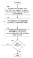
- methods and/or apparatus may provide for establishing a stored test vector, including a plurality of data bits, within a vector data engine (step 1100 ).
- the stored test vector may be transmitted to a memory array (step 1102 ).
- at least one arithmetic or logical operation may be performed upon the stored test vector (step 1104 ).
- the at least one arithmetic or logical operation may be performed by a vector data generator within the vector data engine to update the stored test vector.
- the steps of transmitting 1102 and performing 1104 may be repeated at decision step 1106 so as to continuously transmit continuously changing stored test vectors to the memory array.
- the steps of repeating the transmitting and performing steps may be conducted automatically upon receiving at least one clock pulse.
Landscapes
- Engineering & Computer Science (AREA)
- Power Engineering (AREA)
- General Engineering & Computer Science (AREA)
- Physics & Mathematics (AREA)
- General Physics & Mathematics (AREA)
- Tests Of Electronic Circuits (AREA)
Abstract
Description
| Time: | Signal values of first four output pins. | ||
| 1 | 0001 | ||
| 2 | 0010 | ||
| 3 | 0100 | ||
| 4 | 1000 | ||
Claims (34)
Priority Applications (1)
| Application Number | Priority Date | Filing Date | Title |
|---|---|---|---|
| US11/691,838 US7673196B2 (en) | 2007-03-27 | 2007-03-27 | Methods and apparatus for communicating with a target circuit |
Applications Claiming Priority (1)
| Application Number | Priority Date | Filing Date | Title |
|---|---|---|---|
| US11/691,838 US7673196B2 (en) | 2007-03-27 | 2007-03-27 | Methods and apparatus for communicating with a target circuit |
Publications (2)
| Publication Number | Publication Date |
|---|---|
| US20080244341A1 US20080244341A1 (en) | 2008-10-02 |
| US7673196B2 true US7673196B2 (en) | 2010-03-02 |
Family
ID=39796396
Family Applications (1)
| Application Number | Title | Priority Date | Filing Date |
|---|---|---|---|
| US11/691,838 Expired - Fee Related US7673196B2 (en) | 2007-03-27 | 2007-03-27 | Methods and apparatus for communicating with a target circuit |
Country Status (1)
| Country | Link |
|---|---|
| US (1) | US7673196B2 (en) |
Cited By (1)
| Publication number | Priority date | Publication date | Assignee | Title |
|---|---|---|---|---|
| US20080178054A1 (en) * | 2007-01-24 | 2008-07-24 | Byong-Kwon Lee | Test circuits of semiconductor memory device for multi-chip testing and method for testing multi chips |
Families Citing this family (7)
| Publication number | Priority date | Publication date | Assignee | Title |
|---|---|---|---|---|
| US7954020B2 (en) | 2007-06-06 | 2011-05-31 | Sony Computer Entertainment Inc. | Method and apparatus for testing a circuit |
| US7921346B2 (en) * | 2008-10-31 | 2011-04-05 | International Business Machines Corporation | Verification of array built-in self-test (ABIST) design-for-test/design-for-diagnostics (DFT/DFD) |
| KR101294852B1 (en) * | 2010-10-13 | 2013-08-08 | 엘지디스플레이 주식회사 | Micro Controller, Driving Method thereof and Display Device using the same |
| US9639356B2 (en) * | 2013-03-15 | 2017-05-02 | Qualcomm Incorporated | Arbitrary size table lookup and permutes with crossbar |
| KR101564965B1 (en) * | 2015-05-14 | 2015-11-03 | 주식회사 티맥스 소프트 | Method and server for assigning relative order to message using vector clock and delivering the message based on the assigned relative order under distributed environment |
| US11823758B2 (en) | 2021-02-10 | 2023-11-21 | Taiwan Semiconductor Manufacturing Company, Ltd. | Conducting built-in self-test of memory macro |
| US12033710B2 (en) * | 2021-02-10 | 2024-07-09 | Taiwan Semiconductor Manufacturing Company, Ltd. | System and method for conducting built-in self-test of memory macro |
Citations (2)
| Publication number | Priority date | Publication date | Assignee | Title |
|---|---|---|---|---|
| US7058865B2 (en) * | 2003-02-26 | 2006-06-06 | Renesas Technology Corp. | Apparatus for testing semiconductor integrated circuit |
| US20080304343A1 (en) * | 2007-06-06 | 2008-12-11 | Sony Computer Entertainment Inc. | Method and apparatus for testing a circuit |
-
2007
- 2007-03-27 US US11/691,838 patent/US7673196B2/en not_active Expired - Fee Related
Patent Citations (2)
| Publication number | Priority date | Publication date | Assignee | Title |
|---|---|---|---|---|
| US7058865B2 (en) * | 2003-02-26 | 2006-06-06 | Renesas Technology Corp. | Apparatus for testing semiconductor integrated circuit |
| US20080304343A1 (en) * | 2007-06-06 | 2008-12-11 | Sony Computer Entertainment Inc. | Method and apparatus for testing a circuit |
Cited By (2)
| Publication number | Priority date | Publication date | Assignee | Title |
|---|---|---|---|---|
| US20080178054A1 (en) * | 2007-01-24 | 2008-07-24 | Byong-Kwon Lee | Test circuits of semiconductor memory device for multi-chip testing and method for testing multi chips |
| US7971117B2 (en) * | 2007-01-24 | 2011-06-28 | Samsung Electronics Co., Ltd. | Test circuits of semiconductor memory device for multi-chip testing and method for testing multi chips |
Also Published As
| Publication number | Publication date |
|---|---|
| US20080244341A1 (en) | 2008-10-02 |
Similar Documents
| Publication | Publication Date | Title |
|---|---|---|
| US7673196B2 (en) | Methods and apparatus for communicating with a target circuit | |
| US4404519A (en) | Testing embedded arrays in large scale integrated circuits | |
| US4754215A (en) | Self-diagnosable integrated circuit device capable of testing sequential circuit elements | |
| US8145964B2 (en) | Scan test circuit and scan test control method | |
| KR101405690B1 (en) | Robust memory link testing using memory controller | |
| US6510530B1 (en) | At-speed built-in self testing of multi-port compact sRAMs | |
| US7231563B2 (en) | Method and apparatus for high speed testing of latch based random access memory | |
| JPH097393A (en) | Memory testing device for microelectronic integrated circuit | |
| KR100717207B1 (en) | Weighted random pattern test using pre-stored weights | |
| JPH0480350B2 (en) | ||
| US7954020B2 (en) | Method and apparatus for testing a circuit | |
| US7681096B2 (en) | Semiconductor integrated circuit, BIST circuit, design program of BIST circuit, design device of BIST circuit and test method of memory | |
| KR20040047612A (en) | Method for testing semiconductor memory device and test circuit for semiconductor memory device | |
| US6327683B1 (en) | Device scan testing | |
| JP2005332555A (en) | Test circuit, test method and semiconductor integrated circuit device | |
| JPH0587890A (en) | Semiconductor integrated circuit | |
| US20080133989A1 (en) | Method And Apparatus For Scan Chain Circuit AC Test | |
| CN114460447B (en) | Self-test circuit and self-test method of latch | |
| JP4388641B2 (en) | Integrated circuit testing equipment | |
| JP3339479B2 (en) | Clock control circuit and method | |
| US6804803B2 (en) | Method for testing integrated logic circuits | |
| JPH09281192A (en) | Self-diagnosis circuit of logic integrated circuit | |
| EP1031995B1 (en) | Built-in self-test circuit for memory | |
| US6629275B1 (en) | Reinstate apparatus and method to recreate data background for testing SRAM | |
| JP2006073917A (en) | Integrated circuit |
Legal Events
| Date | Code | Title | Description |
|---|---|---|---|
| AS | Assignment |
Owner name: SONY COMPUTER ENTERTAINMENT INC., JAPAN Free format text: ASSIGNMENT OF ASSIGNORS INTEREST;ASSIGNOR:YOSHIHARA, HIROSHI;REEL/FRAME:019313/0201 Effective date: 20070502 Owner name: SONY COMPUTER ENTERTAINMENT INC.,JAPAN Free format text: ASSIGNMENT OF ASSIGNORS INTEREST;ASSIGNOR:YOSHIHARA, HIROSHI;REEL/FRAME:019313/0201 Effective date: 20070502 |
|
| FEPP | Fee payment procedure |
Free format text: PAYOR NUMBER ASSIGNED (ORIGINAL EVENT CODE: ASPN); ENTITY STATUS OF PATENT OWNER: LARGE ENTITY |
|
| AS | Assignment |
Owner name: SONY NETWORK ENTERTAINMENT PLATFORM INC., JAPAN Free format text: CHANGE OF NAME;ASSIGNOR:SONY COMPUTER ENTERTAINMENT INC.;REEL/FRAME:027445/0657 Effective date: 20100401 |
|
| AS | Assignment |
Owner name: SONY COMPUTER ENTERTAINMENT INC., JAPAN Free format text: ASSIGNMENT OF ASSIGNORS INTEREST;ASSIGNOR:SONY NETWORK ENTERTAINMENT PLATFORM INC.;REEL/FRAME:027481/0351 Effective date: 20100401 |
|
| REMI | Maintenance fee reminder mailed | ||
| LAPS | Lapse for failure to pay maintenance fees | ||
| STCH | Information on status: patent discontinuation |
Free format text: PATENT EXPIRED DUE TO NONPAYMENT OF MAINTENANCE FEES UNDER 37 CFR 1.362 |
|
| STCH | Information on status: patent discontinuation |
Free format text: PATENT EXPIRED DUE TO NONPAYMENT OF MAINTENANCE FEES UNDER 37 CFR 1.362 |
|
| FP | Lapsed due to failure to pay maintenance fee |
Effective date: 20140302 |