US7667257B2 - Capacitor and process for manufacturing the same - Google Patents
Capacitor and process for manufacturing the same Download PDFInfo
- Publication number
- US7667257B2 US7667257B2 US11/585,203 US58520306A US7667257B2 US 7667257 B2 US7667257 B2 US 7667257B2 US 58520306 A US58520306 A US 58520306A US 7667257 B2 US7667257 B2 US 7667257B2
- Authority
- US
- United States
- Prior art keywords
- upper electrode
- dielectric
- lower electrode
- trench
- electrode
- Prior art date
- Legal status (The legal status is an assumption and is not a legal conclusion. Google has not performed a legal analysis and makes no representation as to the accuracy of the status listed.)
- Expired - Fee Related, expires
Links
- 239000003990 capacitor Substances 0.000 title claims abstract description 74
- 238000000034 method Methods 0.000 title claims abstract description 39
- 230000008569 process Effects 0.000 title claims description 24
- 238000004519 manufacturing process Methods 0.000 title claims description 21
- BPUBBGLMJRNUCC-UHFFFAOYSA-N oxygen(2-);tantalum(5+) Chemical compound [O-2].[O-2].[O-2].[O-2].[O-2].[Ta+5].[Ta+5] BPUBBGLMJRNUCC-UHFFFAOYSA-N 0.000 claims abstract description 70
- 229910001936 tantalum oxide Inorganic materials 0.000 claims abstract description 70
- NRTOMJZYCJJWKI-UHFFFAOYSA-N Titanium nitride Chemical compound [Ti]#N NRTOMJZYCJJWKI-UHFFFAOYSA-N 0.000 claims abstract description 51
- 229910021420 polycrystalline silicon Inorganic materials 0.000 claims description 18
- 229910052721 tungsten Inorganic materials 0.000 claims description 16
- 239000010937 tungsten Substances 0.000 claims description 16
- 230000015572 biosynthetic process Effects 0.000 claims description 14
- 238000000231 atomic layer deposition Methods 0.000 claims description 12
- WFKWXMTUELFFGS-UHFFFAOYSA-N tungsten Chemical compound [W] WFKWXMTUELFFGS-UHFFFAOYSA-N 0.000 claims description 12
- RTAQQCXQSZGOHL-UHFFFAOYSA-N Titanium Chemical compound [Ti] RTAQQCXQSZGOHL-UHFFFAOYSA-N 0.000 claims description 9
- 239000000758 substrate Substances 0.000 claims description 9
- 229910052719 titanium Inorganic materials 0.000 claims description 9
- TWNQGVIAIRXVLR-UHFFFAOYSA-N oxo(oxoalumanyloxy)alumane Chemical compound O=[Al]O[Al]=O TWNQGVIAIRXVLR-UHFFFAOYSA-N 0.000 claims description 8
- 239000010936 titanium Substances 0.000 claims description 8
- 229910052751 metal Inorganic materials 0.000 claims description 7
- 239000002184 metal Substances 0.000 claims description 7
- KJTLSVCANCCWHF-UHFFFAOYSA-N Ruthenium Chemical compound [Ru] KJTLSVCANCCWHF-UHFFFAOYSA-N 0.000 claims description 5
- 229910052707 ruthenium Inorganic materials 0.000 claims description 5
- 239000004065 semiconductor Substances 0.000 claims description 4
- 229910021332 silicide Inorganic materials 0.000 claims description 4
- FVBUAEGBCNSCDD-UHFFFAOYSA-N silicide(4-) Chemical compound [Si-4] FVBUAEGBCNSCDD-UHFFFAOYSA-N 0.000 claims description 4
- 150000001875 compounds Chemical class 0.000 claims description 3
- 239000000463 material Substances 0.000 claims description 3
- 230000007547 defect Effects 0.000 abstract description 4
- 238000001039 wet etching Methods 0.000 abstract 1
- 239000010408 film Substances 0.000 description 161
- XUIMIQQOPSSXEZ-UHFFFAOYSA-N Silicon Chemical compound [Si] XUIMIQQOPSSXEZ-UHFFFAOYSA-N 0.000 description 57
- 229910052710 silicon Inorganic materials 0.000 description 57
- 239000010703 silicon Substances 0.000 description 57
- 238000001312 dry etching Methods 0.000 description 23
- 239000011229 interlayer Substances 0.000 description 19
- VYPSYNLAJGMNEJ-UHFFFAOYSA-N Silicium dioxide Chemical compound O=[Si]=O VYPSYNLAJGMNEJ-UHFFFAOYSA-N 0.000 description 17
- 229910052814 silicon oxide Inorganic materials 0.000 description 17
- QGZKDVFQNNGYKY-UHFFFAOYSA-N Ammonia Chemical compound N QGZKDVFQNNGYKY-UHFFFAOYSA-N 0.000 description 16
- 238000005229 chemical vapour deposition Methods 0.000 description 15
- 229910052581 Si3N4 Inorganic materials 0.000 description 14
- HQVNEWCFYHHQES-UHFFFAOYSA-N silicon nitride Chemical compound N12[Si]34N5[Si]62N3[Si]51N64 HQVNEWCFYHHQES-UHFFFAOYSA-N 0.000 description 14
- 238000005755 formation reaction Methods 0.000 description 13
- 238000010438 heat treatment Methods 0.000 description 13
- IJGRMHOSHXDMSA-UHFFFAOYSA-N Atomic nitrogen Chemical compound N#N IJGRMHOSHXDMSA-UHFFFAOYSA-N 0.000 description 12
- 238000005530 etching Methods 0.000 description 11
- 229920002120 photoresistant polymer Polymers 0.000 description 10
- QVGXLLKOCUKJST-UHFFFAOYSA-N atomic oxygen Chemical compound [O] QVGXLLKOCUKJST-UHFFFAOYSA-N 0.000 description 9
- 229910052760 oxygen Inorganic materials 0.000 description 9
- 239000001301 oxygen Substances 0.000 description 9
- 239000002994 raw material Substances 0.000 description 9
- KRHYYFGTRYWZRS-UHFFFAOYSA-N Fluorane Chemical compound F KRHYYFGTRYWZRS-UHFFFAOYSA-N 0.000 description 8
- 238000000151 deposition Methods 0.000 description 7
- 239000010410 layer Substances 0.000 description 7
- 229910021529 ammonia Inorganic materials 0.000 description 6
- 230000008901 benefit Effects 0.000 description 6
- 230000008021 deposition Effects 0.000 description 6
- 239000007789 gas Substances 0.000 description 6
- 230000001965 increasing effect Effects 0.000 description 6
- 229910052757 nitrogen Inorganic materials 0.000 description 6
- CBENFWSGALASAD-UHFFFAOYSA-N Ozone Chemical compound [O-][O+]=O CBENFWSGALASAD-UHFFFAOYSA-N 0.000 description 5
- 238000011156 evaluation Methods 0.000 description 5
- 238000001459 lithography Methods 0.000 description 5
- 230000015654 memory Effects 0.000 description 5
- 229910021341 titanium silicide Inorganic materials 0.000 description 5
- XJDNKRIXUMDJCW-UHFFFAOYSA-J titanium tetrachloride Chemical compound Cl[Ti](Cl)(Cl)Cl XJDNKRIXUMDJCW-UHFFFAOYSA-J 0.000 description 5
- BLRPTPMANUNPDV-UHFFFAOYSA-N Silane Chemical compound [SiH4] BLRPTPMANUNPDV-UHFFFAOYSA-N 0.000 description 4
- 238000010521 absorption reaction Methods 0.000 description 4
- QPJSUIGXIBEQAC-UHFFFAOYSA-N n-(2,4-dichloro-5-propan-2-yloxyphenyl)acetamide Chemical compound CC(C)OC1=CC(NC(C)=O)=C(Cl)C=C1Cl QPJSUIGXIBEQAC-UHFFFAOYSA-N 0.000 description 4
- 229910000069 nitrogen hydride Inorganic materials 0.000 description 4
- 125000004430 oxygen atom Chemical group O* 0.000 description 4
- -1 tungsten nitride Chemical class 0.000 description 4
- 229910052782 aluminium Inorganic materials 0.000 description 3
- XAGFODPZIPBFFR-UHFFFAOYSA-N aluminium Chemical compound [Al] XAGFODPZIPBFFR-UHFFFAOYSA-N 0.000 description 3
- 239000003795 chemical substances by application Substances 0.000 description 3
- 238000002425 crystallisation Methods 0.000 description 3
- 230000008025 crystallization Effects 0.000 description 3
- 239000012212 insulator Substances 0.000 description 3
- 238000002955 isolation Methods 0.000 description 3
- 238000005121 nitriding Methods 0.000 description 3
- 230000002093 peripheral effect Effects 0.000 description 3
- XKRFYHLGVUSROY-UHFFFAOYSA-N Argon Chemical compound [Ar] XKRFYHLGVUSROY-UHFFFAOYSA-N 0.000 description 2
- KZBUYRJDOAKODT-UHFFFAOYSA-N Chlorine Chemical compound ClCl KZBUYRJDOAKODT-UHFFFAOYSA-N 0.000 description 2
- ZAMOUSCENKQFHK-UHFFFAOYSA-N Chlorine atom Chemical compound [Cl] ZAMOUSCENKQFHK-UHFFFAOYSA-N 0.000 description 2
- XYFCBTPGUUZFHI-UHFFFAOYSA-N Phosphine Chemical compound P XYFCBTPGUUZFHI-UHFFFAOYSA-N 0.000 description 2
- OAICVXFJPJFONN-UHFFFAOYSA-N Phosphorus Chemical compound [P] OAICVXFJPJFONN-UHFFFAOYSA-N 0.000 description 2
- 229910021417 amorphous silicon Inorganic materials 0.000 description 2
- 239000000460 chlorine Substances 0.000 description 2
- 229910052801 chlorine Inorganic materials 0.000 description 2
- 239000000470 constituent Substances 0.000 description 2
- 238000011161 development Methods 0.000 description 2
- 230000000694 effects Effects 0.000 description 2
- 230000006870 function Effects 0.000 description 2
- 238000004518 low pressure chemical vapour deposition Methods 0.000 description 2
- 239000007800 oxidant agent Substances 0.000 description 2
- 230000003647 oxidation Effects 0.000 description 2
- 238000007254 oxidation reaction Methods 0.000 description 2
- 229910052698 phosphorus Inorganic materials 0.000 description 2
- 239000011574 phosphorus Substances 0.000 description 2
- 230000000979 retarding effect Effects 0.000 description 2
- JLTRXTDYQLMHGR-UHFFFAOYSA-N trimethylaluminium Chemical compound C[Al](C)C JLTRXTDYQLMHGR-UHFFFAOYSA-N 0.000 description 2
- GGMAUXPWPYFQRB-UHFFFAOYSA-N 1,1,2,2,3,3,4,4-octafluorocyclopentane Chemical compound FC1(F)CC(F)(F)C(F)(F)C1(F)F GGMAUXPWPYFQRB-UHFFFAOYSA-N 0.000 description 1
- CPELXLSAUQHCOX-UHFFFAOYSA-N Hydrogen bromide Chemical compound Br CPELXLSAUQHCOX-UHFFFAOYSA-N 0.000 description 1
- 229910052786 argon Inorganic materials 0.000 description 1
- 238000004380 ashing Methods 0.000 description 1
- 230000004888 barrier function Effects 0.000 description 1
- 238000006243 chemical reaction Methods 0.000 description 1
- 238000004140 cleaning Methods 0.000 description 1
- 239000004020 conductor Substances 0.000 description 1
- 230000007423 decrease Effects 0.000 description 1
- 230000003247 decreasing effect Effects 0.000 description 1
- 238000009792 diffusion process Methods 0.000 description 1
- 238000002474 experimental method Methods 0.000 description 1
- 230000010354 integration Effects 0.000 description 1
- 238000005259 measurement Methods 0.000 description 1
- 150000002736 metal compounds Chemical class 0.000 description 1
- 238000005268 plasma chemical vapour deposition Methods 0.000 description 1
- 238000005498 polishing Methods 0.000 description 1
- 230000009467 reduction Effects 0.000 description 1
- 229920006395 saturated elastomer Polymers 0.000 description 1
- 238000004528 spin coating Methods 0.000 description 1
- 239000000126 substance Substances 0.000 description 1
- 229910052715 tantalum Inorganic materials 0.000 description 1
- GUVRBAGPIYLISA-UHFFFAOYSA-N tantalum atom Chemical compound [Ta] GUVRBAGPIYLISA-UHFFFAOYSA-N 0.000 description 1
- HSXKFDGTKKAEHL-UHFFFAOYSA-N tantalum(v) ethoxide Chemical compound [Ta+5].CC[O-].CC[O-].CC[O-].CC[O-].CC[O-] HSXKFDGTKKAEHL-UHFFFAOYSA-N 0.000 description 1
- 239000010409 thin film Substances 0.000 description 1
- 238000012546 transfer Methods 0.000 description 1
- FAQYAMRNWDIXMY-UHFFFAOYSA-N trichloroborane Chemical compound ClB(Cl)Cl FAQYAMRNWDIXMY-UHFFFAOYSA-N 0.000 description 1
Images


Classifications
-
- H—ELECTRICITY
- H10—SEMICONDUCTOR DEVICES; ELECTRIC SOLID-STATE DEVICES NOT OTHERWISE PROVIDED FOR
- H10B—ELECTRONIC MEMORY DEVICES
- H10B12/00—Dynamic random access memory [DRAM] devices
- H10B12/01—Manufacture or treatment
- H10B12/09—Manufacture or treatment with simultaneous manufacture of the peripheral circuit region and memory cells
-
- H—ELECTRICITY
- H01—ELECTRIC ELEMENTS
- H01L—SEMICONDUCTOR DEVICES NOT COVERED BY CLASS H10
- H01L28/00—Passive two-terminal components without a potential-jump or surface barrier for integrated circuits; Details thereof; Multistep manufacturing processes therefor
- H01L28/40—Capacitors
- H01L28/60—Electrodes
- H01L28/82—Electrodes with an enlarged surface, e.g. formed by texturisation
- H01L28/90—Electrodes with an enlarged surface, e.g. formed by texturisation having vertical extensions
- H01L28/91—Electrodes with an enlarged surface, e.g. formed by texturisation having vertical extensions made by depositing layers, e.g. by depositing alternating conductive and insulating layers
-
- H—ELECTRICITY
- H10—SEMICONDUCTOR DEVICES; ELECTRIC SOLID-STATE DEVICES NOT OTHERWISE PROVIDED FOR
- H10B—ELECTRONIC MEMORY DEVICES
- H10B12/00—Dynamic random access memory [DRAM] devices
- H10B12/01—Manufacture or treatment
- H10B12/02—Manufacture or treatment for one transistor one-capacitor [1T-1C] memory cells
- H10B12/03—Making the capacitor or connections thereto
- H10B12/033—Making the capacitor or connections thereto the capacitor extending over the transistor
Definitions
- the present invention relates to a capacitor that constitutes DRAM and a process for manufacturing the same, in particular, to a capacitor structure suitable for eliminating the problem of the collapse of the lower electrode, which is caused when forming a lower electrode having a crown shape, and a process for manufacturing the same.
- DRAM dynamic random access memory
- gigabit-class memories with a minimum feature size of 100 nm are being commercialized, and moreover, development of DRAMs with a minimum feature size of 90 nm or smaller are being proceeded with. With such miniaturization of semiconductor devices, it has become difficult to ensure desired capacity of capacitors, which are principal constituents of DRAMs.
- a capacitor having a crown structure has been examined, in which a trench (deep hole) is formed in an insulating film, both the inside and outside walls of a lower electrode formed on the inside face of the trench are exposed, and the both sides thereof are used as a capacitor.
- the capacitor having a crown structure it is possible to ensure capacitor area about two times larger than that of a capacitor in which only the inside face of the trench is used. Accordingly, the capacitor having a crown structure offers the advantage that it has capacity two times higher than that of a capacitor in which a lower electrode is provided only on the inside face of the trench.
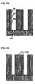
- FIGS. 1A to 1C schematically show the manufacturing process of a crown-structure capacitor.
- a silicon plug 103 is formed in a specified region of a first inter layer dielectric 101 , and a silicon nitride film 102 and a second inter layer dielectric 104 consisting of a thick silicon oxide film are deposited.
- a trench 105 is formed by lithography and dry etching to expose the surface of the silicon plug 103 and then a lower electrode 106 is formed on the inside face of trench.
- FIG. 1A a silicon plug 103 is formed in a specified region of a first inter layer dielectric 101 , and a silicon nitride film 102 and a second inter layer dielectric 104 consisting of a thick silicon oxide film are deposited.
- a trench 105 is formed by lithography and dry etching to expose the surface of the silicon plug 103 and then a lower electrode 106 is formed on the inside face of trench.
- the second inter layer dielectric 104 which supports and surrounds the outside walls of the lower electrode 106 is removed using a hydrofluoric acid (HF) solution.
- HF hydrofluoric acid
- the lower electrode 106 loses its support and its mechanical strength significantly decreases.
- the lower electrode 106 collapses due to the surface tension of the HF solution, causing a pair bit defect, because the adjacent lower electrodes are brought into contact with each other. If the silicon oxide film can be removed by dry etching, which causes no surface tension, the collapse of the lower electrode 106 is effectively prevented.
- no practical technique has been realized yet which makes it possible to remove only the silicon oxide film without damaging the shape of the lower electrode.
- FIGS. 2A to 2G show the manufacturing process of a crown-structure capacitor which is described in Example of the above described patent specification. In the following, the manufacturing process of the crown-structure capacitor described in the patent specification will be explained with reference to FIGS. 2A to 2G .
- a silicon plug 103 is formed in a specified region of a first inter layer dielectric 101 , a silicon nitride film 102 and a second inter layer dielectric 104 consisting of a thick silicon oxide film are deposited.
- a trench 105 is formed so that the surface of the silicon plug 103 is exposed, and after that a first upper electrode 107 made of polycrystalline silicon is formed on the side wall of the trench 105 .
- a first dielectric 108 consisting of stacked film made of tantalum oxide and silicon oxide is deposited on the whole surface and then a outside lower electrode 109 made of titanium nitride is deposited and stacked on the whole surface.
- the outside lower electrode 109 and the first dielectric 108 which are formed on the surface other than the surface of the trench and on the trench bottom, are removed using anisotropic dry etching.
- an inside lower electrode 110 made of polycrystalline silicon is deposited and the inside of the trench is filled with a photoresist 111 .
- the photoresist 111 is formed so that its top surface is positioned a little lower than the top of the trench.
- the inside lower electrode 110 made of polycrystalline silicon and the outside lower electrode 109 made of titanium nitride are subjected to dry etching so that each top surface is almost at the same level as the top surface of the photoresist 111 .
- the photoresist 111 is removed, a second dielectric 112 consisting of a stacked film made of tantalum oxide and silicon oxide is deposited, and a second upper electrode 113 made of titanium nitride is deposited on the whole surface so that the trench is filled up with the electrode, followed by etching back so that the top surface of the second upper electrode 113 is at the level shown in the figure.
- the exposed portion of the second dielectric 112 is subjected to dry etching so that the top surface of the second dielectric 112 is almost at the same level as the top surface of the second upper electrode 113 .
- the first dielectric 108 undergoes etching simultaneously, whereby the top of the first upper electrode 107 is exposed.
- a third upper electrode 114 made of titanium nitride is deposited on the whole surface so that the first upper electrode 107 and the second upper electrode 113 are connected with each other.
- the lower electrode connected with the silicon plug 103 is constructed by the inside lower electrode 110 made of polycrystalline silicon and the outside lower electrode 109 made of titanium nitride.
- first dielectric 108 consisting of a stacked film made of tantalum oxide and silicon oxide is provided between the first upper electrode 107 and the outside lower electrode 109
- second dielectric 112 consisting of a stacked film made of tantalum oxide and silicon oxide is provided between the second upper electrode 113 and the inside lower electrode 110 , whereby a capacitor having a crown structure is made up in the inside of the trench.
- This known example offers the advantage of being capable of preventing the collapse of its lower electrode, because the insulating film constituting the trench is not removed.
- FIG. 3A shows the state after the photoresist 111 , which is filled into the inside of the trench after deposition of the inside lower electrode 110 made of polycrystalline silicon in the step shown in FIG. 2C , has been removed by etching back employing dry etching.
- Etching back is intended to selectively etch the outside lower electrode 109 made of titanium nitride and the inside lower electrode 110 made of polycrystalline silicon so that their top surfaces are made lower as shown in FIG. 2D .
- the first upper electrode 107 is unintentionally etched together and its top surface is also made lower.
- the etching progresses on both the first upper electrode 107 and the inside lower electrode 110 since the first upper electrode 107 is made of polycrystalline silicon just like the inside lower electrode 110 .
- the first dielectric 108 projects from the top surface, forming a vacant space 115 over the first upper electrode 107 .
- the vacant space 115 is filled with the second dielectric 112 , resulting in the formation of an insulating film on the top surface of the first upper electrode 107 .
- the inside upper electrode 113 is formed in this state.
- the second dielectric 116 which is the second dielectric 112 remaining in the vacant space 115 , is formed on the first upper electrode 107 , whereby the top surface of the first upper electrode 107 is not exposed.
- the object of the present invention is to provide a capacitor having a crown structure which aims at electrical connection between upper electrodes by easier and simpler method utilizing an insulating property of tantalum oxide and a process for manufacturing the same.
- the present inventor has found that a tantalum oxide film is brought to the conducting state when it is formed on a titanium or titanium nitride film. Based on this finding, the inventor hit on a crown-structure capacitor formed in an inside of a trench in which a first upper electrode and a second upper electrode are electrically connected via the tantalum oxide film in the conducting state, and has finally accomplished the present invention.
- a capacitor of the present invention is that which comprises at least a lower electrode, a dielectric and an upper electrode:
- the upper electrode comprises a first upper electrode and a second upper electrode
- the first upper electrode has a portion where the first upper electrode is opposite to the second upper electrode via the dielectric
- the first upper electrode and the second upper electrode are electrically connected with each other via the dielectric which is in the conducting state at the portion where the first upper electrode is opposite to the second upper electrode.
- the capacitor of the present invention is that which is formed in the inside of a trench formed in an insulating film and comprises the lower electrode, the dielectric and the upper electrode:
- the lower electrode has a crown structure having an outside face and an inside face
- the upper electrode comprises the first upper electrode which is opposite to the outside face of the lower electrode, and the dielectric and the second upper electrode which extend from the inside face of the lower electrode to the surface other than the surface of the trench;
- the first upper electrode and the second upper electrode are electrically connected with each other via the dielectric which is in the conducting state at the portion where the first upper electrode is opposite to the second upper electrode.
- the capacitor of the present invention is that wherein on the outside face of the lower electrode, a first capacitor region is provided which comprises a first dielectric formed in contact with the outside face of the lower electrode and a first upper electrode formed on the side face of the trench opposite to the lower electrode,
- a second capacitor region which comprises a second dielectric formed in contact with the inside face of the lower electrode and a second upper electrode formed in contact with the second dielectric,
- the second dielectric and the second upper electrode extend on the surface other than the surface of the trench
- the capacitor of the present invention is that wherein the second dielectric is made of tantalum oxide.
- the capacitor of the present invention is that wherein the first upper electrode is made of titanium or titanium nitride and the dielectric is made of tantalum oxide.
- the capacitor of the present invention is that wherein the lower electrode is made of at least one material selected from the group consisting of polycrystalline silicon, metal silicide, tungsten and the compounds thereof, and ruthenium.
- a process for manufacturing a capacitor of the present invention is that which comprises a conductive plug connected to the surface of a semiconductor substrate and a lower electrode which is connected to the conductive plug, comprising at least:
- the process for manufacturing the capacitor of the present invention is that wherein the first upper electrode is electrically connected with the second upper electrode via the second dielectric which is in the conducting state at the portion where the second dielectric is in contact with the upper end of the first upper electrode.
- the process for manufacturing the capacitor of the present invention is that wherein the first upper electrode is made of titanium or titanium nitride, the first dielectric comprises at least aluminum oxide formed by atomic layer deposition, and the second dielectric is made of tantalum oxide.
- the process for manufacturing a capacitor of the present invention is that further comprising a step of heat treating in the temperature range of 600° C. to 750° C., after the formation of the second dielectric made of tantalum oxide.
- the first upper electrode is constructed by the titanium or titanium nitride film
- the second dielectric is constructed by the tantalum oxide film so that it extends on the first upper electrode, whereby the tantalum oxide film in contact with the upper end of the first upper electrode is in the conducting state.
- the first upper electrode can be electrically connected with the second upper electrode via the tantalum oxide film in the conducting state.
- the insulating film that constitutes a trench is not removed, whereby the capacity increasing effect, which is characteristic of a crown-structure capacitor, can be obtained while eliminating the problem of the lower electrode collapse and simplifying the manufacturing steps.
- FIGS. 1A to 1C are cross-sectional views of a series of steps to explain a problem caused when forming a crown structure by conventional process
- FIGS. 2A to 2G are cross-sectional views of a series of steps to explain Example described in Japanese Patent Application Laid-Open No. 10-173148;
- FIGS. 3A to 3D are cross-sectional views of a series of steps to explain a problem in Example described in Japanese Patent Application Laid-Open No. 10-173148;
- FIGS. 4A and 4B are cross-sectional views of samples used for evaluation to explain Example 1 of the present invention.
- FIG. 5 is the evaluation results (current-voltage characteristics) to explain Example 1 of the present invention.
- FIG. 6 is a cross-sectional view of a DRAM to explain Example 2 of the present invention.
- FIGS. 7A to 7L are cross-sectional views of a series of steps to explain Example 3 of the present invention.
- FIG. 7M is an enlarged cross-sectional view of FIG. 7K ;
- FIGS. 8A and 8B are cross-sectional views of a series of steps to supplementarily explain the application of Example 3 of the present invention.
- Example 1 the insulating property of tantalum oxide will be explained in Example 1.
- Example 2 The structure of a DRAM including the capacitor of the present invention will be explained in Example 2, and the process for manufacturing the capacitor of the present invention will be explained in Example 3.
- FIGS. 4A and 4B are cross-sectional views showing the structures of the samples used for the evaluation of the insulating property of tantalum oxide.
- FIG. 4A is that for the case where a lower electrode is made of polycrystalline silicon (sample A)
- FIG. 4B is that for the case where a lower electrode is made of titanium nitride (sample B).
- An element isolation region 202 was formed on the surface of an n-type silicon substrate 201 by a well-known selective oxidation process (LOCOS: Local Oxidation of Silicon). Then, the native oxide layer on the surface of the exposed silicon substrate was removed. After that, a polycrystalline silicon film containing 3 ⁇ 10 20 cm ⁇ 3 of phosphorus was deposited by CVD (Chemical Vapor Deposition) method in which monosilane (SiH 4 ) and phosphine (PH 3 ) were used as raw material gases. The polycrystalline silicon film was treated by known lithography and dry etching to form a prescribed pattern as a capacitor lower electrode 203 .
- CVD Chemical Vapor Deposition
- the surface of the lower electrode 203 was subjected to cleaning treatment in a solution containing hydrofluoric acid (HF) and heat treated for 1 minute in an atmosphere of ammonia (NH 3 ) at 750° C. to form a silicon nitride film with the thickness of 1 nm (not shown in the figure) on the surface of the lower electrode 203 .
- HF hydrofluoric acid
- NH 3 ammonia
- a tantalum oxide film 204 which was to be a dielectric of the capacitor, was deposited through the following procedures.
- CVD method was used in which pentaethoxytantalum (PET/Ta(OC 2 H 5 ) 5 ) as a raw material and oxygen (O 2 ) as an oxidizing agent were employed.
- the conditions of CVD were 430° C. for the temperature and 0.5 Torr for the pressure.
- the tantalum oxide film was deposited to the thickness of 4 nm, and after that the tantalum oxide film was heat treated in an atmosphere of ozone-containing oxygen at 550° C. for 1 minute and further heat treated in an atmosphere of nitrogen at 750° C. for 2 minutes to crystallize the tantalum oxide.
- the tantalum oxide film immediately after deposited under the above conditions was in the amorphous state and its specific dielectric constant was about 25. However, the crystallization increased the specific dielectric constant of the tantalum oxide to 50. And the heat treatment allowed a silicon oxynitride film with the thickness of several nm to be formed in the interface of the lower electrode 203 , which is made of polycrystalline silicon, and the tantalum oxide film 204 .
- a tantalum oxide film was further deposited to the thickness of 8 nm so that they were stacked under the same conditions as above.
- Tantalum oxide has the property of undergoing epitaxial growth when deposited on a crystallized tantalum oxide film, and the above tantalum oxide film with the thickness of 8 nm had been completely crystallized right after its deposition. Accordingly, heat treatment for crystallization of stacked tantalum oxide was not fundamentally necessary. However, in this Example, heat treatment was performed in an atmosphere of nitrogen at 650° C. for 1 minute, for comparison with the sample B.
- a titanium nitride film which was to be an upper electrode 205 , was deposited.
- CVD method was used in which titanium chloride (TiCl 4 ) as a raw material and ammonia (NH 3 ) as a nitriding agent were employed.
- the conditions of CVD were 550° C. for the temperature and 1 Torr for the pressure.
- the film thickness of the titanium nitride film was 40 nm.
- the titanium nitride film was treated by lithography and dry etching to form a prescribed pattern as an upper electrode 205 .
- the titanium silicide film was formed by forming plasma of titanium chloride at 550° C. and depositing titanium atom on the surface of the substrate while allowing silicide formation to progress.
- the thickness of the titanium silicide film was 10 nm.
- FIG. 5 shows the current-voltage characteristics of the capacitors having the structure of each of the sample A and the sample B.
- the figure plots a voltage Vpl applied to the upper electrode as the abscissa and a leak current per unit area as the ordinate.
- capacitors having a three-dimensional structure which are applied to gigabit-class DRAMs allowable leak current values are required to be 1 ⁇ 10 ⁇ 9 (A/cm 2 ) or lower at ⁇ 1.0 V.
- the characteristic indicated by “sample A” in the figure is that of the capacitor whose lower electrode is made of polycrystalline silicon, while the characteristic indicated by “sample B” is that of the capacitor whose lower electrode is made of titanium nitride.
- the leak current values were as small as about 2 ⁇ 10 ⁇ 10 (A/cm 2 ) at both +1.0 V and ⁇ 1.0 V. This indicates that satisfactory insulating property can be obtained. Further, the sample A was not broken, but stable when applying a voltage of ⁇ 5.0 V. On the other hand, in the sample B whose lower electrode is made of titanium nitride, even at a low voltage of ⁇ 1.0 V, the leak current was observed whose values were much larger than those in the range of ordinary current evaluation, and thus, its insulating property was not observed. This indicates that the tantalum oxide film on the titanium nitride film was in the completely conducting state.
- the reason that the sample B was made conductive is that oxygen atoms that constitute tantalum oxide are absorbed by the titanium in the titanium nitride film. Specifically, the number of oxygen-vacancy defects is increased in the tantalum oxide film, and current flows through the defects. Particularly the tantalum oxide film in the amorphous state shows a significant tendency toward this phenomenon. This phenomenon becomes significant when the deposited tantalum oxide film undergoes heat treatment at about 650° C., though the phenomenon has already occurred in the tantalum oxide deposition step at about 400° C., and the tantalum oxide film is brought to the almost completely conducting state. The same phenomenon occurs when the lower electrode is made up of titanium instead of titanium nitride.
- the lower electrode is made of silicon.
- oxygen atoms absorbed from tantalum oxide react with the silicon to form a silicon oxide film in the interface of the tantalum oxide film and the lower electrode.
- the formed silicon oxide film retards the absorption of oxygen atoms from the tantalum oxide, whereby the reaction is saturated.
- titanium nitride this saturation phenomenon is not observed.
- the electrode already has a silicon nitride film formed on its surface and the silicon nitride film functions as a barrier to oxygen diffusion; as a result, the effect of retarding oxygen atom absorption is enhanced.
- the silicon oxide film formed in the interface functions as an obstacle to leak current generation, and thus, it is rather effective in reduction of leak current.
- the tantalum oxide film formed by CVD method has been described in this Example, the same results are obtained for a tantalum oxide film formed by ALD (Atomic Layer Deposition) method.
- the tantalum oxide film formed by ALD method is also in the amorphous state right after formation. If the tantalum oxide film undergoes heat treatment at about 650° C., irrespective of atmosphere, the tantalum oxide film on titanium nitride film can be brought to the conducting state due to the above described oxygen absorption phenomenon.
- FIG. 6 is a schematic cross-sectional view of a DRAM having a first aluminum interconnect layer formed therein.
- a p-type silicon substrate 301 In a p-type silicon substrate 301 was formed an n-well 302 and in the inside of the n-well 302 was formed a first p-well 303 . In the region other than the n-well 302 was formed a second p-well 304 so that an element isolation region 305 was formed.
- the first p-well 303 shows a memory array region where a plurality of memory cells are arranged and the second p-well 304 shows a peripheral circuit region.
- the transistor 306 was made up of a drain 308 , a source 309 and a gate electrode 311 via a gate insulator 310 .
- the transistor 307 was made up of the source 309 , which is common to each transistor, a drain 312 and a gate electrode 311 via a gate insulator 310 .
- An insulating film 313 having flat surface was provided in such a manner as to cover each transistor.
- a silicon plug 315 made of polycrystalline silicon was provided in a contact hole 314 formed in a specified region of the insulating film 313 in such a manner as to be connected to the source 309 .
- a bit line contact consisting of a titanium silicide film 316 , a titanium nitride film 317 and a tungsten film 318 was provided and a bit line consisting of a tungsten nitride film 319 and a tungsten film 320 was provided in such a manner as to be connected to the bit line contact.
- a first inter layer dielectric 321 having flat surface was provided in such a manner as to cover the bit line.
- a silicon plug 322 was provided in a contact hole formed in a specified region of each of the insulating film 313 and the first inter layer dielectric 321 in such a manner as to be connected to each of the drain 308 and 312 of the transistor.
- a trench (deep hole) 325 was formed in a specified region of each of a silicon nitride film 323 on the first inter layer dielectric 321 and a second inter layer dielectric 324 .
- a first upper electrode 326 made of titanium nitride and on the side face of the first upper electrode 326 was provided a first dielectric 327 .
- a lower electrode 328 made of polycrystalline silicon was formed on the inside face and the bottom surface of the first dielectric 327 , to be connected to the silicon plug 322 .
- a second dielectric 329 made of tantalum oxide was formed on the whole surface including the surface of the lower electrode 328 and a second upper electrode 330 was formed on the whole surface of the second dielectric 329 .
- a third inter layer dielectric 331 was formed in such a manner as to cover the capacitor.
- a transistor constituting a peripheral circuit which was made up of a source 309 , a drain 312 , a gate insulator 310 and a gate electrode 311 .
- a contact hole 332 was formed in such a manner as to be connected to the drain 312 .
- a contact plug consisting of a titanium silicide film 316 , a titanium nitride film 317 and a tungsten film 318 was provided, and on the contact plug was formed a first interconnect layer consisting of a tungsten nitride film 319 and a tungsten film 320 .
- a part of the first interconnect layer was connected to a second interconnect layer consisting of a titanium nitride film 336 , an aluminum film 337 and a titanium nitride film 338 via a titanium nitride film 334 and a tungsten film 335 , which were filled into a contact hole 333 formed in such a manner as to pass through a first inter layer dielectric 321 , a silicon nitride film 323 , a second inter layer dielectric 324 and a third inter layer dielectric 331 .
- An upper electrode 330 of the capacitor, which was provided in the memory array region, in part of the region was led out as a lead interconnect 339 into the peripheral circuit region. And, it was connected to a second interconnect layer consisting of a titanium nitride film 342 , an aluminum film 343 and a titanium nitride film 344 via a titanium nitride film 340 and a tungsten film 341 , which were filled into the contact hole formed in the specified region of the third inter layer dielectric 331 . Then, formations of an inter layer dielectric, a contact and an interconnect layer was repeated depending on its needs to make up a DRAM.
- a capacitor which includes a crown-structure lower electrode having an outside face and an inside face with the second inter layer dielectric forming the trench being left, in which a first capacitor region having a first dielectric and a first upper electrode made of titanium nitride is provided on the outside face of the crown-structure lower electrode, and a second capacitor region having a second dielectric made of tantalum oxide and a second upper electrode is provided on the inside face of the crown-structure lower electrode.
- the first upper electrode made of titanium nitride can be electrically connected to the second upper electrode, though it is in such a position that it is out of contact with the second upper electrode due to the intervention of the second dielectric made of tantalum oxide, because the tantalum oxide film in contact with the titanium nitride film is in the conducting state.
- FIGS. 7A to 7L are cross-sectional views of a series of steps in the crown-structure capacitor manufacturing process of the present invention.
- FIG. 7M is an enlarged view of FIG. 7K .
- a silicon plug 322 was formed in a specified region of a first inter layer dielectric 321 by a well-known process and then a silicon nitride film 323 with the thickness of 50 nm was formed on the surface, by a well-known process, LPCVD (Low Pressure Chemical Vapor Deposition) method.
- LPCVD Low Pressure Chemical Vapor Deposition
- a silicon oxide film 324 with the thickness of 2000 nm was formed by a well-known process, plasma CVD method, and a silicon film 345 with the thickness of 500 nm was formed so as to be stacked on the silicon oxide film 324 by a well-known process, CVD method.
- the silicon film 345 was used as a hard mask when the subjecting silicon oxide film 324 to dry etching. After this, a photoresist pattern was formed on the silicon film 345 by lithography, though it is not shown in the figure. Then, the silicon film 345 was etched by a well-known process, plasma dry etching, using the photoresist pattern as a mask to transfer the pattern to the silicon film 345 .
- the dry etching of the silicon film was performed using a mixed gas of chlorine (Cl 2 ), hydrogen bromide (HBr) and oxygen (O 2 ) where the pressure was 10 mTorr and the plasma power was 100 W.
- the conditions may be changed properly as long as the silicon film can be etched.
- the silicon oxide film 324 with the thickness of 2000 nm was etched by dry etching using the silicon film 345 , which had the pattern transferred, as a mask, to form a trench 325 .
- the dry etching of the silicon oxide film was performed using a mixed gas of octafluorocyclopentane (C 5 F 8 ), argon (Ar) and oxygen (O 2 ) where the pressure is 100 mTorr and the plasma power is 1500 W.
- the silicon film 345 which was used as a hard mask, was removed by isotropic dry etching. In this removing operation, when the silicon film 345 is left thick, the silicon plug 322 exposed to the inside of the trench might be unintentionally etched. To avoid this, it is possible, in the trench formation operation, to remove the silicon film 345 remaining at the stage where the silicon nitride film 323 is exposed, and then etching the silicon nitride film. Employing CMP (Chemical Mechanical Polishing) method also makes it possible to selectively remove the silicon film 345 on the surface while avoiding etching of the silicon plug.
- CMP Chemical Mechanical Polishing
- the CVD method was performed using titanium chloride (TiCl 4 ) as a raw material and ammonia (NH 3 ) as a nitriding agent where the pressure is 1 Torr and the temperature is 550° C.
- the titanium nitride film formed on the surface other than the surface of the trench and on the trench bottom was removed by dry etching to form the first upper electrode 326 on the side wall of the trench.
- the dry etching of the titanium nitride film was performed using a mixed gas of chlorine (Cl 2 ) and boron chloride (BCl 3 ) where the pressure is 10 mTorr and the plasma power is 100 W.
- the silicon plug 322 might be unintentionally etched, however, it is substantially no problem because the film thickness of the titanium nitride film is small.
- the aluminum oxide film was formed by atomic layer deposition (ALD: Atomic Layer Deposition) method using trimethylaluminum (TMA: Al(CH 3 ) 3 ) as a raw material gas and ozone (O 3 ) as an oxidizing agent.
- ALD Atomic Layer Deposition
- TMA trimethylaluminum
- O 3 ozone
- the basic steps which consist of raw material feeding, exhaust, ozone feeding and exhaust were taken as a cycle and the cycle was repeated 60 times to form the aluminum oxide with the thickness of 6 nm.
- the raw material and ozone were fed while keeping the pressure at 0.5 Torr and the temperature at 350° C. Since the efficiency of deposition by ALD method is very low, it is preferable to employ batch treatment, in which a plurality of substrates can be treated simultaneously.
- the conditions of ALD method can be changed variously.
- the phosphorus-doped silicon film was formed by CVD method.
- the silicon film containing 3 ⁇ 10 20 cm ⁇ 3 of phosphorus was deposited using monosilane (SiH 4 ) and phosphine (PH 3 ) as raw material gases where the pressure was 1 Torr and the temperature was 520° C.
- the silicon film deposited under the above conditions is amorphous and has the advantage of having very smooth surface.
- the silicon film and the aluminum oxide film formed on the surface other than the surface of the trench and on the trench bottom were removed by dry etching to form the first dielectric 327 , which was in contact with the first upper electrode 326 , and the outside lower electrode 328 a .
- the surface of the silicon plug 322 was exposed.
- This dry etching can be performed under the same conditions as those employed for dry etching of silicon film used as a hard mask.
- the deposition conditions were the same as those employed for the formation of the outside lower electrode 328 a .
- a treatment was done for removing the native oxide film formed on the surface of the silicon plug 322 and the outside lower electrode 328 a;
- a photoresist 346 was formed on the whole surface by spin coating and then subjected to exposure and development to allow the photoresist 346 to remain in the inside of the trench alone.
- the silicon film exposed on the surface was removed by dry etching. Subsequently after that, the photoresist was removed by oxygen ashing. At this stage, a lower electrode made up of the inside lower electrode 328 b , which was connected to the silicon plug 322 , and the outside lower electrode 328 a , which was connected to the inside lower electrode, had been formed. A first capacitor region made up of the outside lower electrode 328 a , the first dielectric 327 and the first upper electrode 326 had been also formed.
- a tantalum oxide film which was to be a second dielectric 329 , was deposited by CVD method under the same conditions as those employed in Example 1.
- the tantalum oxide film with the thickness of 4 nm was deposited, and the tantalum oxide film was heat treated in an atmosphere of ozone-containing oxygen at 550° C. for 1 minute and further heat treated in an atmosphere of nitrogen at 750° C. for 2 minutes to be crystallized.
- a tantalum oxide film with the thickness of 8 nm was deposited so that they were stacked under the same conditions. After that, the tantalum oxide film was heat treated in an atmosphere of nitrogen at 650° C. for 1 minute.
- FIG. 7M is an enlarged view of FIG. 7K .
- the portion of the second dielectric 329 made of tantalum oxide, which is in contact with the upper end of the first upper electrode 326 made of titanium nitride became a conducting tantalum oxide film 328 a.
- the lower electrode ( 328 a and 328 b ) made of phosphorus-doped amorphous silicon can be polycrystallized by the above heat treatment, to be changed to a conductor.
- the lower electrode may be polycrystallized before the formation of the tantalum oxide film.
- a titanium nitride film which was to be a second upper electrode 330 , was deposited.
- CVD method using titanium chloride (TiCl 4 ) as a raw material and ammonia (NH 3 ) as a nitriding agent was applied.
- the CVD method was performed at the temperature of 550° C. and at the pressure of 1 Torr.
- the upper electrode may be formed by stacking another metal film, such as a tungsten film, on the titanium nitride film.
- a crown-structure capacitor could be formed which includes: a first capacitor region made up of the outside lower electrode 328 a, the first dielectric 327 and the first upper electrode 326 ; and a second capacitor region made up of the inside lower electrode 328 b , the second dielectric 329 and the second upper electrode 330 .
- the first upper electrode and the second upper electrode are electrically connected with each other by utilizing the property of tantalum oxide which is brought to the conducting state when it is on the titanium nitride film, whereby an advantage can be obtained that a crown-structure capacitor can be manufactured easily and simply without employing complicated dry etching processes, which are described in the known prior application.
- the tantalum oxide film was formed after the formations of the first upper electrode, the first dielectric and the lower electrode, and underwent heat treatment at 750° C. to be crystallized.
- the first upper electrode is formed at 550° C. and the first dielectric at 350° C.
- heat treatment at 750° C. warping of the first dielectric might result due to the difference in degree of denseness, causing increase of the leak current.
- it is effective to perform heat treatment in an atmosphere of ammonia or nitrogen at 750° C. for 1 minute after the formation of the first upper electrode and to perform heat treatment in an atmosphere of nitrogen at 700° C. for 1 minute after the formation of the first dielectric. In other words, it is effective to perform heat treatment whenever each film is formed, thereby making the film dense.
- a metal such as tungsten or ruthenium, or a metal compound such as tungsten nitride may also be used.
- the lower electrode is conductive when it is formed, heat treatment for crystallization is not required.
- an amorphous silicon film with the thickness of 10 nm or smaller can sometimes be difficult to crystallize, but the use of a metal or the like has the advantage of eliminating such a problem.
- the use of tungsten, tungsten nitride or ruthenium for the lower electrode also produces the effect of retarding leak current, because it prevents the absorption of oxygen from tantalum oxide as described in Example 1.
- ALD method can also be used for forming the first upper electrode, the metal lower electrode or the tantalum oxide film.
- a thin film with the thickness of 10 nm or less can be formed with good controllability, giving the advantage of being applicable even when the width of the trench is decreased to accommodate increasing integration density of DRAMs.
- the silicon nitride film 323 was also etched to expose the silicon plug 322 .
- the silicon plug 322 was exposed to an etching atmosphere, though the degree was low, when removing the silicon film used as a hard mask, when dry etching the titanium nitride film which was to be the first upper electrode, or when etching the silicon film which was to be the outside lower electrode.
- the silicon nitride film 323 is effective to allow the silicon nitride film 323 to remain, as shown in FIGS. 8A and 8B . Specifically, the silicon nitride film 323 remains, until the first upper electrode 326 , the first dielectric 327 and the outside lower electrode 328 a are formed, to cover the surface of the silicon plug 322 ( FIG. 8A ). Then, the silicon nitride film 323 may be etched right before the formation of the inside lower electrode, to expose the silicon plug so that the inside lower electrode 328 b is formed ( FIG. 8B ).
Landscapes
- Engineering & Computer Science (AREA)
- Power Engineering (AREA)
- Manufacturing & Machinery (AREA)
- Computer Hardware Design (AREA)
- Microelectronics & Electronic Packaging (AREA)
- Semiconductor Memories (AREA)
Abstract
Description
Claims (11)
Applications Claiming Priority (2)
| Application Number | Priority Date | Filing Date | Title |
|---|---|---|---|
| JP2005329606A JP2007141904A (en) | 2005-11-15 | 2005-11-15 | Capacitor and its manufacturing method |
| JP2005-329606 | 2005-11-15 |
Publications (2)
| Publication Number | Publication Date |
|---|---|
| US20070108493A1 US20070108493A1 (en) | 2007-05-17 |
| US7667257B2 true US7667257B2 (en) | 2010-02-23 |
Family
ID=38039842
Family Applications (1)
| Application Number | Title | Priority Date | Filing Date |
|---|---|---|---|
| US11/585,203 Expired - Fee Related US7667257B2 (en) | 2005-11-15 | 2006-10-24 | Capacitor and process for manufacturing the same |
Country Status (2)
| Country | Link |
|---|---|
| US (1) | US7667257B2 (en) |
| JP (1) | JP2007141904A (en) |
Families Citing this family (9)
| Publication number | Priority date | Publication date | Assignee | Title |
|---|---|---|---|---|
| KR100760632B1 (en) * | 2006-03-03 | 2007-09-20 | 삼성전자주식회사 | Method of forming a capacitor |
| TWI283458B (en) * | 2006-04-04 | 2007-07-01 | Promos Technologies Inc | Method for preparing a capacitor structure of a semiconductor memory |
| JP2010251406A (en) * | 2009-04-13 | 2010-11-04 | Elpida Memory Inc | Semiconductor device and manufacturing method thereof |
| JP2013030557A (en) * | 2011-07-27 | 2013-02-07 | Elpida Memory Inc | Method of manufacturing semiconductor device |
| CN106328376A (en) * | 2015-07-03 | 2017-01-11 | 华硕电脑股份有限公司 | Manufacturing method of capacitor |
| TWI581441B (en) * | 2015-09-08 | 2017-05-01 | 力晶科技股份有限公司 | Multilayer crown-shaped mim capacitor and manufacturing method thereof |
| CN108550568B (en) * | 2018-04-26 | 2020-04-10 | 长鑫存储技术有限公司 | Capacitor array, forming method thereof and semiconductor device |
| US11610894B2 (en) * | 2019-06-28 | 2023-03-21 | Intel Corporation | Capacitor separations in dielectric layers |
| CN115706110A (en) * | 2021-08-10 | 2023-02-17 | 长鑫存储技术有限公司 | Semiconductor structure, layout thereof and semiconductor device |
Citations (4)
| Publication number | Priority date | Publication date | Assignee | Title |
|---|---|---|---|---|
| JPH10173148A (en) | 1996-12-13 | 1998-06-26 | Hitachi Ltd | Semiconductor storage device |
| US20040227175A1 (en) * | 2003-03-19 | 2004-11-18 | Shinpei Iijima | Semiconductor integrated circuit device and method of manufacturing the device |
| US20040248362A1 (en) * | 2003-02-14 | 2004-12-09 | Elpida Memory, Inc. | Semiconductor device and fabrication method therefor |
| US20060234510A1 (en) * | 2005-04-14 | 2006-10-19 | Elpida Memory, Inc. | Semiconductor memory device and method for manufacturing semiconductor memory device |
Family Cites Families (5)
| Publication number | Priority date | Publication date | Assignee | Title |
|---|---|---|---|---|
| JP2956482B2 (en) * | 1994-07-29 | 1999-10-04 | 日本電気株式会社 | Semiconductor memory device and method of manufacturing the same |
| JP4737789B2 (en) * | 1999-06-18 | 2011-08-03 | 株式会社東芝 | Semiconductor device |
| JP2002222934A (en) * | 2001-01-29 | 2002-08-09 | Nec Corp | Semiconductor device and manufacturing method thereof |
| JP2003124348A (en) * | 2001-10-17 | 2003-04-25 | Elpida Memory Inc | Semiconductor device and its manufacturing method |
| JP2004363396A (en) * | 2003-06-05 | 2004-12-24 | Renesas Technology Corp | Semiconductor device and manufacturing method thereof |
-
2005
- 2005-11-15 JP JP2005329606A patent/JP2007141904A/en active Pending
-
2006
- 2006-10-24 US US11/585,203 patent/US7667257B2/en not_active Expired - Fee Related
Patent Citations (4)
| Publication number | Priority date | Publication date | Assignee | Title |
|---|---|---|---|---|
| JPH10173148A (en) | 1996-12-13 | 1998-06-26 | Hitachi Ltd | Semiconductor storage device |
| US20040248362A1 (en) * | 2003-02-14 | 2004-12-09 | Elpida Memory, Inc. | Semiconductor device and fabrication method therefor |
| US20040227175A1 (en) * | 2003-03-19 | 2004-11-18 | Shinpei Iijima | Semiconductor integrated circuit device and method of manufacturing the device |
| US20060234510A1 (en) * | 2005-04-14 | 2006-10-19 | Elpida Memory, Inc. | Semiconductor memory device and method for manufacturing semiconductor memory device |
Also Published As
| Publication number | Publication date |
|---|---|
| JP2007141904A (en) | 2007-06-07 |
| US20070108493A1 (en) | 2007-05-17 |
Similar Documents
| Publication | Publication Date | Title |
|---|---|---|
| US7667257B2 (en) | Capacitor and process for manufacturing the same | |
| KR101275025B1 (en) | Wiring structure for a semiconductor device and method of forming the same | |
| US5164337A (en) | Method of fabricating a semiconductor device having a capacitor in a stacked memory cell | |
| US5843818A (en) | Methods of fabricating ferroelectric capacitors | |
| KR100418573B1 (en) | Method for fabricating semiconductor device | |
| US7332395B2 (en) | Method of manufacturing a capacitor | |
| JP4221421B2 (en) | Semiconductor device and manufacturing method thereof | |
| US7547628B2 (en) | Method for manufacturing capacitor | |
| US6165841A (en) | Method for fabricating capacitors with hemispherical grains | |
| US20020160565A1 (en) | Capacitor for semiconductor devices and a method of fabricating such capacitors | |
| US7071056B2 (en) | Method of forming a dual-sided capacitor | |
| KR100796724B1 (en) | Capacitor and method of manufacturing the same | |
| JP4053226B2 (en) | Semiconductor integrated circuit device and manufacturing method thereof | |
| US20040126963A1 (en) | Capacitor fabrication method | |
| KR20020031283A (en) | Integrated Circuit Device And Method For Manufacture The Same | |
| US6503810B2 (en) | Method for forming a capacitor for semiconductor devices with an amorphous LixTa1-xO3 dieletric layer having a perovskite structure | |
| US20090197384A1 (en) | Semiconductor memory device and method for manufacturing semiconductor memory device | |
| US20070269979A1 (en) | Method of forming a pattern and method of manufacturing a semiconductor device using the same | |
| JP2001053250A (en) | Semiconductor device and its manufacture | |
| US20080124887A1 (en) | Method for manufacturing semiconductor device | |
| JP4497260B2 (en) | Semiconductor integrated circuit device and manufacturing method thereof | |
| JP2001223343A (en) | Lower electrode of capacitor and its manufacturing method | |
| JP4298187B2 (en) | Manufacturing method of semiconductor device | |
| KR20070044929A (en) | Method for fabricating capacitor in semiconductor device | |
| KR100384843B1 (en) | Method for fabricating capacitor |
Legal Events
| Date | Code | Title | Description |
|---|---|---|---|
| AS | Assignment |
Owner name: ELPIDA MEMORY, INC,JAPAN Free format text: ASSIGNMENT OF ASSIGNORS INTEREST;ASSIGNOR:IIJIMA, SHINPEI;REEL/FRAME:018460/0453 Effective date: 20061013 |
|
| CC | Certificate of correction | ||
| FPAY | Fee payment |
Year of fee payment: 4 |
|
| AS | Assignment |
Owner name: ELPIDA MEMORY INC., JAPAN Free format text: SECURITY AGREEMENT;ASSIGNOR:PS4 LUXCO S.A.R.L.;REEL/FRAME:032414/0261 Effective date: 20130726 |
|
| AS | Assignment |
Owner name: PS4 LUXCO S.A.R.L., LUXEMBOURG Free format text: ASSIGNMENT OF ASSIGNORS INTEREST;ASSIGNOR:ELPIDA MEMORY, INC.;REEL/FRAME:032895/0001 Effective date: 20130726 |
|
| FEPP | Fee payment procedure |
Free format text: PAYOR NUMBER ASSIGNED (ORIGINAL EVENT CODE: ASPN); ENTITY STATUS OF PATENT OWNER: LARGE ENTITY |
|
| AS | Assignment |
Owner name: PS5 LUXCO S.A.R.L., LUXEMBOURG Free format text: ASSIGNMENT OF ASSIGNORS INTEREST;ASSIGNOR:PS4 LUXCO S.A.R.L.;REEL/FRAME:039818/0506 Effective date: 20130829 Owner name: LONGITUDE SEMICONDUCTOR S.A.R.L., LUXEMBOURG Free format text: CHANGE OF NAME;ASSIGNOR:PS5 LUXCO S.A.R.L.;REEL/FRAME:039793/0880 Effective date: 20131112 |
|
| FEPP | Fee payment procedure |
Free format text: MAINTENANCE FEE REMINDER MAILED (ORIGINAL EVENT CODE: REM.) |
|
| LAPS | Lapse for failure to pay maintenance fees |
Free format text: PATENT EXPIRED FOR FAILURE TO PAY MAINTENANCE FEES (ORIGINAL EVENT CODE: EXP.) |
|
| STCH | Information on status: patent discontinuation |
Free format text: PATENT EXPIRED DUE TO NONPAYMENT OF MAINTENANCE FEES UNDER 37 CFR 1.362 |
|
| FP | Lapsed due to failure to pay maintenance fee |
Effective date: 20180223 |