US7656744B2 - Memory module with load capacitance added to clock signal input - Google Patents
Memory module with load capacitance added to clock signal input Download PDFInfo
- Publication number
- US7656744B2 US7656744B2 US11/611,036 US61103606A US7656744B2 US 7656744 B2 US7656744 B2 US 7656744B2 US 61103606 A US61103606 A US 61103606A US 7656744 B2 US7656744 B2 US 7656744B2
- Authority
- US
- United States
- Prior art keywords
- clock signal
- load capacity
- signal
- data strobe
- phase
- Prior art date
- Legal status (The legal status is an assumption and is not a legal conclusion. Google has not performed a legal analysis and makes no representation as to the accuracy of the status listed.)
- Expired - Fee Related, expires
Links
Images


Classifications
-
- G—PHYSICS
- G11—INFORMATION STORAGE
- G11C—STATIC STORES
- G11C5/00—Details of stores covered by group G11C11/00
- G11C5/06—Arrangements for interconnecting storage elements electrically, e.g. by wiring
- G11C5/063—Voltage and signal distribution in integrated semi-conductor memory access lines, e.g. word-line, bit-line, cross-over resistance, propagation delay
-
- G—PHYSICS
- G11—INFORMATION STORAGE
- G11C—STATIC STORES
- G11C5/00—Details of stores covered by group G11C11/00
- G11C5/02—Disposition of storage elements, e.g. in the form of a matrix array
- G11C5/04—Supports for storage elements, e.g. memory modules; Mounting or fixing of storage elements on such supports
Definitions
- the present invention relates to a memory module, and in particular to a memory module optimal for use in a multiple-rank memory system.
- Memory systems are employed various types of electronic equipment such as personal computers (hereafter, referred to as “PCs”), digital cameras, and printers, and their memory capacity has been increased more and more.
- PCs personal computers
- DIMMs dual inline memory modules
- Each of the DIMMs has terminals on the opposite surfaces of a module board, and is provided with semiconductor memories, a phase-locked loop circuit (PLL) for phase adjustment, a register for supplying a control signal, and so on.
- PLL phase-locked loop circuit
- the semiconductor memories used here are large-capacity dynamic random access memories (DRAM).
- the memory system is optimized for relevant electronic equipment by properly determining a memory capacity, a number of data bits, and a number of ranks, and is provided with a single or a plurality of memory modules.
- a rank means a group of memories that can be read and written simultaneously.
- FIG. 1 shows a schematic diagram of a three-slot memory system.
- the memory system includes a motherboard that is provided thereon with a memory controller 1 , and a plurality of wirings including data or data strobe (DQ/DQS) signal lines 2 and clock (CLK) signal lines 3 . Because data, data strobe and clock signals are differential or complementary signals, the signal lines 2 and 3 are depicted as signal line pairs.
- DQ/DQS data or data strobe
- CLK clock
- the memory system of FIG. 1 further includes a connector 4 and a DIMM 5 in each slot.
- the DIMM 5 has a plurality of DRAMs 6 , a PLL 7 , and a register 8 mounted on the memory module board.
- the DIMM 5 is also referred to as the “registered DIMM”.
- each of the CLK signal lines 3 is connected to one of the DIMMs 5 .
- each of the DQ/DQS signal lines 2 is connected to all of the DIMMs 5 by being branched therefrom.
- FIG. 2 is a topology diagram illustrating the CLK signal lines 3 in this memory system.
- FIGS. 3 and 4 are topology diagrams illustrating the DQ/DQS signal lines 2 when one-rank and two-rank DIMMs are used in the memory system, respectively.
- the CLK signal lines 3 are connected such that a CLK signal is supplied to the PLL 7 of each DIMM 5 from the memory controller 1 via the corresponding pair of CLK signal lines 3 and the corresponding connector 4 on the motherboard.
- the DQ/DQS signal lines 2 are branched from the motherboard wirings and connected to the DRAMs 6 of the entire DIMMs 5 via the respective connectors 4 .
- a DQ/DQS signal is supplied to one DRAM of each DIMM 5 .
- a DQ/DQS signal is supplied to two DRAMs (RANK 0 and RANK 1 ) of each DIMM.
- CLK signal lines 3 ” and “DQ/DQS signal lines 2 ” are used herein to generally refer to the wirings including internal wirings of the DIMMs 5 .
- FIG. 5 shows an example of the CLK signal lines 3 in the registered DIMM 5
- FIG. 6 shows an example of the DQS signal lines 2 in the registered DIMM 5
- a CLK signal output from the memory controller 1 is input to the PLL 7 through CLK terminals 11 of the DIMM 5
- the CLK signal is buffered by the PLL 7 , and input to the register 8 and to the DRAMs 6 mounted on the front and rear surfaces of the DIMM 5
- the CLK signal lines 3 connecting between the PLL 7 and the respective DRAMs 6 in the DIMM 5 are equal in length. Feedback wirings having an equal length to the CLK signal lines 3 connecting between the PLL 7 and the DRAMs 6 are provided to check the delay time in the CLK signal lines 3 of the DIMM 5 .
- a DQS signal output from the memory controller 1 is input to at least one of the DRAMs 6 via corresponding DQS terminals 12 and corresponding stub resistances 13 .
- the CLK signal input to the DRAMs 6 via the PLL 7 is processed by the PLL 7 to enter the DRAMs 6 at the same timing as the timing when the CLK signal enters the PLL 7 . Accordingly, it can be considered that the timing of the CLK signal entering the PLL 7 is the same as the timing of the CLK signal entering the DRAMs 6 .
- the DRAM 6 latches the written data transmitted by the data signal DQ in response to the data strobe signal DQS.
- the CLK signal and the DQS signal are complementary signals (CLK and CLKB, DQS and DQSB), respectively, and their timings are decided based on the respective cross points. Deviation of the cross points that occurs between the CLK signal and the DQS signal when the DRAM 6 latches data during writing is referred to as tDQSS.
- the tDQSS can be reworded as “[the difference in flight time (propagation time) from the memory controller to the DRAM between the CLK signal and the DQS signal]+[the deviation of timing when the CLK signal and the DQS signal are output from the controller]”.
- the tDQSS is desirably small. This is because a large tDQSS will disable the normal transfer of data from the DQS signal to the CLK signal within the DRAM. According to the standard JEDEC DDR2 specification, therefore, the tDQSS is limited to ⁇ 0.25 ⁇ tCK (tCK denotes one cycle time of the CLK signal), and the tDQSS is ⁇ 750 ps in DDR2-667.
- the specification means that the tDQSS becomes smaller as the operating frequency becomes higher. Therefore, it is crucial to reduce the tDQSS in order to increase the operation speed.
- FIG. 7 is an explanatory drawing for explaining relationship among the numbers of DIMMs and ranks forming the memory system and the numbers of CLK and DQS signal loads.
- Table 1 shows the numbers of CLK and DQS signal loads.
- the number of CLK signal loads is one, and the number of DQ/DQS signal loads is one.
- the number of CLK signal loads is one, and the number of DQ/DQS signal loads is two.
- the number of CLK signal loads is one, and the number of DQ/DQS signal loads is four.
- the number of CLK signal loads is one, and the number of DQ/DQS signal loads is four.
- the number of CLK signal loads is one, and the number of DQ/DQS signal loads is eight.
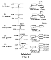
- FIG. 8 is schematic block diagrams showing the memory systems and signal waveform diagrams thereof.
- the DQS signal is delayed by tDQSS 1 relative to the CLK signal when the number of loads is one, delayed by tDQSS 2 when the number of loads is two, and by tDQSS 3 when the number of loads is four.
- the same motherboard is used even after various configuration factors of the memory system (e.g., the number of DIMMs and the number of ranks) have been changed. Therefore, the slew rate (gradient) of the DQS waveform becomes low (the waveform deteriorates) as the number of DIMMs and/or the number of ranks is increased, and the timing at the cross point is delayed.
- the load of the CLK signal is not changed, the waveform of the CLK signal is not changed and the timing at the cross point is not delayed.
- the tDQSS is increased along with the increase of the number of DIMMs and/or the number of ranks, eventually exceeding the tDQSS specification that becomes more severe along with the increase of the operation speed. This may result in breakage of the memory system.
- Patent Publication 1 discloses a technique in which timing of clocks CLK input to a PLL, a register, and DRAMs is adjusted such that a margin of command and address setup time before the CLK is equal to that of command and address hold time after the CLK.
- Patent Publication 2 discloses a technique in which a clock CLK is delayed by phase data derived from a data strobe signal DQS.
- Patent Publication 3 discloses a technique in which delay of a DQS signal relative to an internal clock signal is determined to synchronize data DQ to an internal clock.
- Japanese Laid-Open Patent Publication No. 2004-138480 discloses a test system which is design to eliminate effect of wiring impedance in an LSI tester and a performance board by inputting a data signal at a clock to a first-stage register from a clock selection circuit.
- Japanese Laid-Open Patent Publication No. H11-191019 discloses a clock driver circuit which detects waveform deterioration in an output and changes its drive capacity.
- Patent Publications describe various techniques relating to synchronization to the clock and techniques to correct the output waveform.
- these clock synchronization techniques involve detecting a phase difference, and thus require a circuit for this purpose.
- None of these Patent Publications describe a technique relating to synchronization to a device to which a clock signal is input, or a technique suggesting solutions of the present invention.
- the tDQSS is increased along with the increase of the number DIMMs and/or the number of ranks, eventually exceeding the tDQSS specification that becomes more severe along with the increase of the operation speed, and resulting in breakage of the memory system.
- the present invention basically employs techniques as described below. It is obvious that various changes and modifications that may be made without departing from the sprit or scope of the invention are also included in the present invention.
- a memory module with a multiple-rank configuration includes a phase-locked loop circuit for distributing a clock signal to memories, and a load capacity provided at a clock signal input portion of the phase-locked loop circuit in order to match input timings of a clock signal and a data strobe signal entering each of the memories.
- the load capacity is set such that a time constant of a data strobe signal line represented by a product of a sum of a stub resistance and a wiring impedance in a wiring transmitting the data strobe signal multiplied by an input pin capacity of each memory receiving the data strobe signal is equal to a time constant of a clock signal line represented by a product of a sum of the load capacity and a clock signal input pin capacity of the phase-locked loop circuit multiplied by a wiring impedance of the clock signal.
- the load capacity is added to each of complementary signal lines of the clock signal.
- another load capacity having a half of a capacity value of the load capacity is provided between complementary signal lines of the clock signal as a substitute for the load capacity.
- one end of the load capacity provided within the phase-locked loop circuit is connected to a dummy pin, and a clock signal input pin of the phase-locked loop circuit is connected to the dummy pin.
- the opposite ends of another load capacity having a half of a capacity value of the load capacity and provided within the phase-locked loop circuit as a substitute for the load capacity are connected to dummy pins, respectively, and complementary clock signal input pins of the phase-locked loop circuit are connected to the dummy pins, respectively.
- a layout design for the clock signal within a memory module board including a characteristic impedance, a wiring length, a wiring width, wiring layers, a stub resistance value, terminal ends and so on of a wiring extending between a clock terminal and an input pin of the phase-locked loop circuit is made equal to a layout design for the data strobe signal including a characteristic impedance, a wiring length, a wiring width, wiring layers, a stub resistance value, terminal ends and so on of a wiring extending between a data strobe terminal and an input pin of each memory; and the load capacity is added to the clock signal input portion of the phase-locked loop circuit whereby a total capacity value of data strobe signal input pins of the memories connected to the data strobe signal is made equal to a capacity value of the clock signal input portion of the phase-locked loop circuit.
- the load capacity is set such that a time constant of a data strobe signal line in a signal wiring transmitting the data strobe signal from a memory controller to an input pin of each memory is equal to a time constant of a clock signal line in a signal wiring transmitting the clock signal from the memory controller to an input pin of the phase-locked loop circuit.
- the present invention provides a memory module with a multiple-rank configuration, in which a load capacity is provided at the vicinity of a clock signal input pin of a phase-locked loop circuit to which a clock signal is input to match a time constant of a data strobe signal line with a time constant of a clock signal line.
- the matching of input timings of the clock signal and the data strobe signal input to the memory has an effect to reduce tDQSS and increase the timing margin.
- the components additionally required to implement the invention are only one or two capacities (capacitors) (between CLK and CLKB or to CLK and CLKB) and thus a large occupying area is not required.
- FIG. 1 is a schematic diagram showing a related memory system
- FIG. 2 is a topology diagram showing CLK signal lines in the memory system of FIG. 1 ;
- FIG. 3 is a topology diagram showing DQ/DQS signal lines when a one-rank DIMM is used in the memory system of FIG. 1 ;
- FIG. 4 is a topology diagram showing DQ/DQS signal lines when two-rank DIMM is used in the memory system of FIG. 1 ;
- FIG. 5 is a diagram showing CLK signal lines in a related registered DIMM
- FIG. 6 is a diagram showing DQS signal lines in the related registered DIMM
- FIG. 7 is an explanatory diagram illustrating numbers of loads of CLK and DQS signals in the memory system
- FIG. 8 shows schematic block diagrams of memory systems and respective waveform diagrams of CLK and DQS signal lines corresponding thereto;
- FIG. 9A is a configuration diagram of a memory system, while FIG. 9B is a graph illustrating flight time (propagation time) of DQS and CLK signals in the memory system of FIG. 9A ;
- FIG. 10A is a schematic block diagram in which a load capacity is added to each CLK signal input portion of a PLL provided in a memory module according to the present invention
- FIG. 10B is a schematic diagram showing impedances of CLK and DQS signal lines of the memory module;
- FIG. 11 shows waveform diagrams of CLK and DQS signal lines and respective schematic block diagrams of memory systems corresponding thereto according to a first embodiment of the present invention
- FIG. 12A is a schematic block diagram in which a load capacity is added between complementary inputs of CLK signals according to a second embodiment of the invention.
- FIG. 12B is a schematic block diagram illustrating a modified example of the memory module of FIG. 12 ;
- FIGS. 13A and 13B show schematic block diagrams showing other examples of the second embodiment in which load capacities are provided at CLK signal input portion in a PLL.
- FIG. 14 is a schematic block diagram showing still another example of the second embodiment in which a load capacity is added to the CLK signal input portions.
- a memory module according to the present invention will be described in detail with reference to FIGS. 9A and 9B .
- the problems entailed by a memory system using a conventional memory module(s) will be analyzed, and then the basic configuration of the memory module according to the present invention will be described based on a result of analysis.
- FIG. 9A is a configuration diagram of a memory system using a conventional memory module(s), and FIG. 9B shows data relating to flight time (propagation time) of DQS and CLK signals in the memory system.
- the present inventor devised the memory module of the present invention based on the data on flight time (propagation time) of the DQS and CLK signals in this conventional memory system.
- the memory system shown in FIG. 9A has a memory controller 1 and three slots on a motherboard 91 , and the controller 1 and three slots are connected to each other by motherboard wirings 92 .
- Each of the slots is provided with a connector 4 into which a corresponding DIMM 5 is inserted.
- the DIMMs 5 are detachable so that a memory system can be formed to have any desired memory capacity and any number of ranks.
- FIG. 9B shows data obtained in memory systems having a registered DIMM(s) by calculating flight times (propagation times) of DQS and CLK signals based on write simulation waveforms from the memory controller 1 to the third slot that is farthest from the memory controller 1 . Differences in propagation time are obtained by comparing the flight times (propagation times) with the flight time when one one-rank DIMM is inserted in the third slot that is used as the reference.
- (A) denotes a memory system used as the reference, in which the first and second slots are vacant and a one-rank DIMM is inserted in the third slot.
- (B) denotes a memory system in which one-rank DIMMs are inserted in all of the first, second, and third slots, respectively.
- (C) denotes a memory system in which the first and second slots are vacant and a two-rank DIMM is inserted in the third slot.
- (D) denotes a memory system in which the first slot is vacant, and two-rank DIMMs are inserted in the second and third slots, respectively.
- the flight time (propagation time) of the CLK signal increases only slightly.
- the difference in flight time (propagation time) of the CLK signal due to the differences in the number of DIMMs and the number of ranks is so small that it can be said that the flight time (propagation time) of the CLK signal does not change significantly.
- the difference between the memory system (A) with one one-rank DIMM (vacant, vacant, and one-rank DIMM) and the memory system (C) with one two-rank DIMM (vacant, vacant, and two-rank DIMM) is about 200 ps.
- the difference between the memory system (A) with one one-rank DIMM (vacant, vacant, and one-rank DIMM) and the memory system (B) with three one-rank DIMMs (one-rank, one-rank, and one-rank DIMMS) is about 60 ps
- the difference between the memory system (C) with one two-rank DIMM (vacant, vacant, and two-rank DIMM) and the memory system (D) with two two-rank DIMMs (vacant, two-rank and two-rank DIMMS) is about 80 ps.
- the wirings in the motherboard and/or memory module are designed such that the wiring impedance of the wirings assumes a rated value in order to propagate the signal waveform correctly.
- the wiring impedance is made larger than the rated wiring impedance value at the positions where the slots are arranged.
- the impedance is connected in parallel to the position of the slot. The setting is made such that the rated wiring impedance is obtained in this state.
- the memory module inserted in the slot is assumed to be a memory module having one memory rank. Accordingly, when a multiple-rank memory module is inserted, a multiplicity of DRAMs is connected in parallel and the wiring impedances at the slots are decreased, whereby the flight time (propagation time) is increased.
- the flight time propagation time
- the increase in the number of DRAMs connected in parallel to the DQS signal lines increases the flight time (propagation time). It is therefore believed that the difference in flight time (propagation time) due to the increase of the number of DIMMs is not significant, whereas the difference in flight time (propagation time) due to the increase of the number of ranks in one slot is large.
- the present invention has been made based on the findings that the DQS signal load varies depending on various memory system configurations whereas the CLK signal load stays stable, and that the number of ranks is more important than the number of DIMMs in terms of the influence to the flight time (propagation time) of the DQS signal.
- the increase in flight time (propagation time) of the DQS signal can be considered as the increase of tDQSS.
- the flight time (propagation time) is increased by about 200 ps, whereas the flight time (propagation time) is increased only by about 60 to 80 ps even if the number of DIMMs is doubled or tripled. It is believed that the influence of the number of ranks to the DQS signal flight time (propagation time) is more important that of the number of DIMMs.
- the difference in flight time (propagation time) between the DQS signal and the CLK signal causes increase of tDQSS, leading to addition of pressure to the timing budget and over-specification. These pose serious obstacles to the increase of operation speed. Accordingly, it is essential to control the difference in flight time (propagation time) between the DQS signal and the CLK signal.
- this control can be done on the DIMMs.
- the same motherboard is used for various different configurations of memory system (in the number of DIMMs or ranks).
- the flight time (propagation time) of the DQS signal is significantly dependent on the number of ranks as described above.
- the restrictions on the wiring occupying area on the memory module or the number of elements other than the memory have become very severe. This is because it is required to mount even more memories in a smaller area as the capacity of the memory module is increased, the size thereof is reduced, and the functions are sophisticated.
- the present inventor has discovered that adding a load capacity to a clock (CLK) signal input portion of the PLL of a multiple-rank memory module is effective to solve the problem above. Similar effects can be expected by adding a capacity to the vicinity of a CLK input portion of a DRAM, or adding a capacity to the vicinity of an output portion of the PLL. In this case, however, the number of required capacities (capacitors) is twice as many as the number of DRAMs mounted on the memory module, leading to increase of the occupying area. When an appropriate capacity is added to the vicinity of the CLK signal input portion of each PLL of a multiple-rank DIMM according to the present invention, only one or two more capacities are additionally required, and thus the increase of the occupying area can be prevented.
- CLK clock
- a load capacity is added to vicinity of a CLK signal input portion of a PLL of a multiple-rank DIMM, the load capacity being according to the number of DRAMs connected in parallel to a DQS signal.
- the addition of the load capacity to the PLL CLK signal input portion matches time constants of input portions between a CLK signal line of the PLL and a DQS signal line of each of the DRAMs.
- the matching of the time constants matches the timing of the CLK signal received by the PLL with the timing of the DQS signal received by the DRAMs.
- the CLK signal enters the DRAMs at the same timing as the CLK signal enters the PLL, the timings of the CLK and DQS signals input to the DRAMs are matched with each other. This reduces the tDQSS, while increasing the timing margin. As a result, a memory module which has multiple ranks and yet does not malfunction at high frequencies can be obtained.
- FIGS. 10A , 10 B and 11 A first embodiment of the present invention will be described with reference to FIGS. 10A , 10 B and 11 .
- a load capacity is added to a CLK signal input portion of a PLL 7 of a memory module 5
- FIG. 10A is a schematic configuration diagram in which the load capacity for timing adjustment is added to each of the CLK signal input portions of the PLL 7
- FIG. 10B is a schematic diagram showing impedances of a CLK signal line and a DQS signal line.
- FIG. 11 shows signal waveform diagrams and schematic block diagrams of corresponding memory systems
- FIG. 10A shows that the PLL has only CLK and CLKB signal input pins 101 and pads 102 , while other components and parts of the PLL are omitted.
- a clock signal is complementary CLK and CLKB signals, which are input to the clock signal input pins 101 of the PLL 7 through the input terminals 11 of the DIMM 5 .
- the load capacity Cadd 14 is added to each of the CLK and CLKB input pins 101 of the CLK and CLKB signal input portions of the PLL 7 .
- Zodd_CLK denotes an odd mode impedance of the CLK signal line pair
- Cpll denotes a CLK signal input capacity of the PLL
- R denotes a resistance value of a DQS signal stub resistance
- Zodd_DQS denotes an odd mode impedance of the DQS signal line pair
- Cdram_all denotes a total sum of DRAM input capacities of the DQS signals connected commonly on the same memory module.
- the left side of the formula (1) represents the time constant of the clock signal line from the input terminal 11 to the CLK input pin 101 of the PLL 7 in the memory module 5 .
- the right side represents the time constant of the data strobe signal line from the input terminal 12 to DQS input pin of the DRAM 6 in the memory module 5 .
- the timings of the CLK signal and the DQS signal entering the DRAM are matched by equalizing these time constants.
- the operation will be described with reference to FIG. 11 .
- a load capacity Cadd satisfying the formula (1) is added to the vicinity of the CLK signal input portion of the PLL, the waveform is deteriorated by the effect of the time constant determined by the wiring (transmission line) and the capacity. This retards the cross point of the CLK signal by time T 1 (or T 2 ) in comparison when no capacity load is added.
- the waveform (A) in FIG. 11 represents a waveform of the CLK signal at the PLL input portion when no capacity load is added (@PLLin).
- the waveform (B) represents a waveform of the CLK signal at the PLL input portion when the capacity load Cadd is added (@PLLin (Cadd)).
- the waveform (C) represents a CLK signal waveform (@DRAMin (Cadd)) at the DRAM input portion when the capacity load Cadd is added.
- the addition of the capacity load Cadd retards the CLK signal by time T 1 (T 2 ).
- T 1 corresponds to an amount of delay for a capacity Cadd 1 in a two-rank memory module
- T 2 corresponds to an amount of delay for a capacity Cadd 2 in a four-rank memory module.
- the waveform (D) represents a DQS signal waveform of the DRAM when one two-rank DIMM is inserted into the slot.
- tDQSS 4 is obtained which is improved by time T 1 in comparison with the tDQSS 2 in FIG. 8 .
- the waveform (E) represents a DQS signal waveform of the DRAM when one four-rank DIMM is inserted into the slot.
- tDQSS 5 is obtained which improved by time T 2 in comparison with the tDQSS 3 in FIG. 8 .
- the CLK signal is improved by the amount of delay T 1 (T 2 ), which reduces the tDQSS and increases the timing margin.
- the load capacity Cadd satisfying the formula (1) is added to the vicinity of the CLK signal input portion of the PLL in the multiple-rank memory module.
- the time constants of the clock signal line and the data strobe signal line in the memory module are equalized by the addition of the load capacity Cadd, whereby the timings of the CLK signal and the DQS signal entering the DRAM are matched with each other.
- the matching of the timings of the CLK signal and the DQS signal entering the DRAM reduces the tDQSS, and thus increases the timing margin.
- a multiple-rank memory module operable at high speed can be provided.
- FIG. 12A is a schematic configuration diagram in which a load capacity is added between the complementary inputs of the CLK signals.
- FIG. 12B shows a modified example of the memory module of FIG. 12A .
- FIGS. 13A and 13B are schematic configuration diagrams in which a load capacity provided in the PLL is added to the CLK signal.
- FIG. 14 is a schematic configuration diagram showing configuration of a memory module that the CLK signal lines and the DQS signal lines are similar in structure and that an additional load capacity is added.
- clock signal input pins 101 corresponding to complementary CLK signal input pair (CLK and CLKB) are connected with a load capacity 14 .
- a half of the capacity value Cadd in the formula (1) will be enough for the load capacity 14 .
- the memory module according to the second embodiment requires only one load capacity having the half capacity value, and hence requires a smaller number of components and a smaller occupying area.
- the load capacity 14 of FIG. 12A may be provided within the PLL together with dummy pins 103 as shown in FIG. 12B .
- the opposite ends of the load capacity 14 are connected to the dummy pins 103 .
- the dummy pins 103 are further connected to the clock signal input pins 101 .
- dummy pins 104 and load capacities Cadd 14 are provided in the PLL 7 .
- One ends of the load capacities Cadd 14 are connected to the dummy pins 104 , respectively.
- the dummy pins 104 are nonconnected pins as shown in FIG. 13A .
- the dummy pins are connected to the CLK and CLKB signal input pins 101 of the PLL 7 on the DIMM 5 .
- the load capacity is added or adjusted so as to equalize the time constant of the clock signal line and the time constant of the data strobe signal line. This eliminates the need of arranging a capacity on the DIMM, and hence reduces the number of components required and reduces the occupying area.
- the load capacity having the half capacity value may be connected between the complementary clock signal pair.
- the layout design for the CLK signal including the characteristic impedance, wiring length, wiring width, wiring layers, stub resistance value, and terminal ends of the wiring extending between the DIMM terminal and the PLL is equalized with the layout design for the DQS signal including the characteristic impedance, wiring length, wiring width, wiring layers, stub resistance value, and terminal ends of the wiring extending between the DIMM terminal and the DRAM.
- a load capacity 14 is added to the CLK input portions of the PLL 7 to match the capacity thereof with the capacity of the DQS input pin portion of the DRAM connected to another DRAM(s) (not shown) in common.
- the characteristics of the CLK signal line between the DIMM terminal and the PLL are matched with the characteristics of the DQS signal line between the DIMM terminal and the DRAM. In this manner, the timings of the clock (CLK) signal received by the PLL and the data strobe (DQS) signal received by the DRAM can be matched with high precision.
- a load capacity Cadd is added to the vicinity of the CLK signal input portion of the PLL in order to equalize the time constant of the clock signal line with the time constant of the data strobe signal line in the memory module.
- approximate values of the wiring length, wiring impedance and the like in the motherboard are publicly known. Therefore, it is also possible to match the time constant of the clock signal lines with the time constant of the data strobe signal lines in consideration of the motherboard.
- the matching of the time constants of the wirings in not only the DIMM but also the motherboard makes it possible to match the timings of the clock (CLK) signal and the data strobe (DQS) signal with even higher precision. As a result, a multiple-rank memory module operable at high speed can be provided,
- the present invention is not limited to the embodiments but may be otherwise variously embodied within the spirit and scope of the invention.
- the embodiments described above include various aspects of the invention, and various inventions may be devised by suitably combining the disclosed constituent requirements. For example, some of the components according to the foregoing embodiments may be omitted as long as the desired effect can be obtained.
Landscapes
- Dram (AREA)
- Memory System (AREA)
Abstract
Description
| TABLE 1 | |||||
| Number of loads when load | |||||
| of one one-rank DIMM is | |||||
| Case | defined as 1 | CLK | DQS | ||
| (A) | 1 one- |
1 | 1 | ||
| (B) | 1 two- |
1 | 2 | ||
| (C) | 2 two- |
1 | 4 | ||
| (D) | 1 four- |
1 | 4 | ||
| (E) | 2 four- |
1 | 8 | ||
Zodd — CLK×(Cadd+Cpll)=(R+Zodd — DQS)×Cdram_all (Formula 1)
Claims (6)
Applications Claiming Priority (2)
| Application Number | Priority Date | Filing Date | Title |
|---|---|---|---|
| JP2005362005A JP2007164599A (en) | 2005-12-15 | 2005-12-15 | Memory module |
| JP2005-362005 | 2005-12-15 |
Publications (2)
| Publication Number | Publication Date |
|---|---|
| US20070140040A1 US20070140040A1 (en) | 2007-06-21 |
| US7656744B2 true US7656744B2 (en) | 2010-02-02 |
Family
ID=38173268
Family Applications (1)
| Application Number | Title | Priority Date | Filing Date |
|---|---|---|---|
| US11/611,036 Expired - Fee Related US7656744B2 (en) | 2005-12-15 | 2006-12-14 | Memory module with load capacitance added to clock signal input |
Country Status (2)
| Country | Link |
|---|---|
| US (1) | US7656744B2 (en) |
| JP (1) | JP2007164599A (en) |
Cited By (2)
| Publication number | Priority date | Publication date | Assignee | Title |
|---|---|---|---|---|
| US9357649B2 (en) | 2012-05-08 | 2016-05-31 | Inernational Business Machines Corporation | 276-pin buffered memory card with enhanced memory system interconnect |
| US9519315B2 (en) | 2013-03-12 | 2016-12-13 | International Business Machines Corporation | 276-pin buffered memory card with enhanced memory system interconnect |
Families Citing this family (7)
| Publication number | Priority date | Publication date | Assignee | Title |
|---|---|---|---|---|
| KR100906999B1 (en) | 2007-06-11 | 2009-07-08 | 주식회사 하이닉스반도체 | Memory modules and memory systems |
| KR101053540B1 (en) | 2010-02-26 | 2011-08-03 | 주식회사 하이닉스반도체 | External signal input circuit of semiconductor memory |
| KR101136984B1 (en) | 2010-03-29 | 2012-04-19 | 에스케이하이닉스 주식회사 | Power supply control circuit and semiconductor apparatus using the same |
| JP2012008684A (en) * | 2010-06-23 | 2012-01-12 | Elpida Memory Inc | Memory module and semiconductor memory device |
| US9557765B2 (en) | 2013-01-22 | 2017-01-31 | Via Technologies, Inc. | Mechanism for automatically aligning data signals and strobe signals on a source synchronous bus |
| US9552320B2 (en) | 2013-01-22 | 2017-01-24 | Via Technologies, Inc. | Source synchronous data strobe misalignment compensation mechanism |
| US9319035B2 (en) * | 2013-01-22 | 2016-04-19 | Via Technologies, Inc. | Source synchronous bus signal alignment compensation mechanism |
Citations (9)
| Publication number | Priority date | Publication date | Assignee | Title |
|---|---|---|---|---|
| US5495435A (en) * | 1993-11-18 | 1996-02-27 | Nec Corporation | Synchronous DRAM memory module |
| JPH11191019A (en) | 1997-12-26 | 1999-07-13 | Oki Electric Ind Co Ltd | Clock driver circuit, semiconductor integrated circuit and clock wiring method |
| US6128748A (en) * | 1998-03-25 | 2000-10-03 | Intel Corporation | Independent timing compensation of write data path and read data path on a common data bus |
| JP2004070800A (en) | 2002-08-08 | 2004-03-04 | Elpida Memory Inc | Memory system and memory module |
| JP2004138480A (en) | 2002-10-17 | 2004-05-13 | Matsushita Electric Ind Co Ltd | Semiconductor device and AC spec inspection method |
| JP2004531981A (en) | 2001-06-25 | 2004-10-14 | ランバス・インコーポレイテッド | Data recovery device for synchronous chip-to-chip system |
| JP2005078547A (en) | 2003-09-03 | 2005-03-24 | Renesas Technology Corp | Semiconductor integrated circuit |
| US7313715B2 (en) * | 2001-02-09 | 2007-12-25 | Samsung Electronics Co., Ltd. | Memory system having stub bus configuration |
| US7457174B2 (en) * | 2005-04-23 | 2008-11-25 | Infineon Technologies Ag | Semiconductor memory and method for adapting the phase relationship between a clock signal and strobe signal during the acceptance of write data to be transmitted |
Family Cites Families (2)
| Publication number | Priority date | Publication date | Assignee | Title |
|---|---|---|---|---|
| TWI228259B (en) * | 2000-05-22 | 2005-02-21 | Samsung Electronics Co Ltd | Method and circuit for inputting and outputting data, and system using semiconductor memory device including the same |
| DE102005032059B3 (en) * | 2005-07-08 | 2007-01-18 | Infineon Technologies Ag | Semiconductor memory module with bus architecture |
-
2005
- 2005-12-15 JP JP2005362005A patent/JP2007164599A/en active Pending
-
2006
- 2006-12-14 US US11/611,036 patent/US7656744B2/en not_active Expired - Fee Related
Patent Citations (10)
| Publication number | Priority date | Publication date | Assignee | Title |
|---|---|---|---|---|
| US5495435A (en) * | 1993-11-18 | 1996-02-27 | Nec Corporation | Synchronous DRAM memory module |
| JPH11191019A (en) | 1997-12-26 | 1999-07-13 | Oki Electric Ind Co Ltd | Clock driver circuit, semiconductor integrated circuit and clock wiring method |
| US6128748A (en) * | 1998-03-25 | 2000-10-03 | Intel Corporation | Independent timing compensation of write data path and read data path on a common data bus |
| US7313715B2 (en) * | 2001-02-09 | 2007-12-25 | Samsung Electronics Co., Ltd. | Memory system having stub bus configuration |
| JP2004531981A (en) | 2001-06-25 | 2004-10-14 | ランバス・インコーポレイテッド | Data recovery device for synchronous chip-to-chip system |
| JP2004070800A (en) | 2002-08-08 | 2004-03-04 | Elpida Memory Inc | Memory system and memory module |
| JP2004138480A (en) | 2002-10-17 | 2004-05-13 | Matsushita Electric Ind Co Ltd | Semiconductor device and AC spec inspection method |
| JP2005078547A (en) | 2003-09-03 | 2005-03-24 | Renesas Technology Corp | Semiconductor integrated circuit |
| US7412616B2 (en) * | 2003-09-03 | 2008-08-12 | Renesas Technology Corp. | Semiconductor integrated circuit |
| US7457174B2 (en) * | 2005-04-23 | 2008-11-25 | Infineon Technologies Ag | Semiconductor memory and method for adapting the phase relationship between a clock signal and strobe signal during the acceptance of write data to be transmitted |
Cited By (2)
| Publication number | Priority date | Publication date | Assignee | Title |
|---|---|---|---|---|
| US9357649B2 (en) | 2012-05-08 | 2016-05-31 | Inernational Business Machines Corporation | 276-pin buffered memory card with enhanced memory system interconnect |
| US9519315B2 (en) | 2013-03-12 | 2016-12-13 | International Business Machines Corporation | 276-pin buffered memory card with enhanced memory system interconnect |
Also Published As
| Publication number | Publication date |
|---|---|
| JP2007164599A (en) | 2007-06-28 |
| US20070140040A1 (en) | 2007-06-21 |
Similar Documents
| Publication | Publication Date | Title |
|---|---|---|
| US11994982B2 (en) | Memory module with distributed data buffers | |
| US7089412B2 (en) | Adaptive memory module | |
| US7274583B2 (en) | Memory system having multi-terminated multi-drop bus | |
| US7079446B2 (en) | DRAM interface circuits having enhanced skew, slew rate and impedance control | |
| US6937494B2 (en) | Memory module, memory chip, and memory system | |
| US11947474B2 (en) | Multi-mode memory module and memory component | |
| EP3447770B1 (en) | High capacity memory system using standard controller component | |
| US7285979B2 (en) | Apparatus and method for independent control of on-die termination for output buffers of a memory device | |
| US7095661B2 (en) | Semiconductor memory module, memory system, circuit, semiconductor device, and DIMM | |
| US8417870B2 (en) | System and method of increasing addressable memory space on a memory board | |
| US7768867B2 (en) | Stacked semiconductor device | |
| US20100309706A1 (en) | Load reduced memory module and memory system including the same | |
| US8064236B2 (en) | Memory module, method for using same and memory system | |
| US6487086B2 (en) | Circuit module | |
| US20130138898A1 (en) | Memory module including plural memory devices and command address register buffer | |
| US20250191626A1 (en) | Data-buffer controller/control-signal redriver | |
| US20100312925A1 (en) | Load reduced memory module | |
| WO2022132538A1 (en) | Signal skew correction in integrated circuit memory devices | |
| US7656744B2 (en) | Memory module with load capacitance added to clock signal input | |
| US20090049324A1 (en) | Methods and systems for operating memory in two modes | |
| US20040100812A1 (en) | Circuit topology for high speed memory access | |
| GB2388691A (en) | Clocking memory banks out of phase to reduce the output noise | |
| US20100299486A1 (en) | Electronic Devices and Methods for Storing Data in a Memory |
Legal Events
| Date | Code | Title | Description |
|---|---|---|---|
| AS | Assignment |
Owner name: ELPIDA MEMORY, INC., JAPAN Free format text: ASSIGNMENT OF ASSIGNORS INTEREST;ASSIGNOR:AOKI, YURIKA;REEL/FRAME:018658/0797 Effective date: 20061208 Owner name: ELPIDA MEMORY, INC.,JAPAN Free format text: ASSIGNMENT OF ASSIGNORS INTEREST;ASSIGNOR:AOKI, YURIKA;REEL/FRAME:018658/0797 Effective date: 20061208 |
|
| AS | Assignment |
Owner name: ELPIDA MEMORY, INC., JAPAN Free format text: ASSIGNMENT OF ASSIGNORS INTEREST;ASSIGNORS:AOKI, YURIKA;FUNABA, SEIJI;NISHIO, YOJI;REEL/FRAME:018825/0569 Effective date: 20061208 Owner name: ELPIDA MEMORY, INC.,JAPAN Free format text: ASSIGNMENT OF ASSIGNORS INTEREST;ASSIGNORS:AOKI, YURIKA;FUNABA, SEIJI;NISHIO, YOJI;REEL/FRAME:018825/0569 Effective date: 20061208 |
|
| FPAY | Fee payment |
Year of fee payment: 4 |
|
| AS | Assignment |
Owner name: ELPIDA MEMORY INC., JAPAN Free format text: SECURITY AGREEMENT;ASSIGNOR:PS4 LUXCO S.A.R.L.;REEL/FRAME:032414/0261 Effective date: 20130726 |
|
| AS | Assignment |
Owner name: PS4 LUXCO S.A.R.L., LUXEMBOURG Free format text: ASSIGNMENT OF ASSIGNORS INTEREST;ASSIGNOR:ELPIDA MEMORY, INC.;REEL/FRAME:032896/0001 Effective date: 20130726 |
|
| AS | Assignment |
Owner name: PS5 LUXCO S.A.R.L., LUXEMBOURG Free format text: ASSIGNMENT OF ASSIGNORS INTEREST;ASSIGNOR:PS4 LUXCO S.A.R.L.;REEL/FRAME:039818/0506 Effective date: 20130829 Owner name: LONGITUDE SEMICONDUCTOR S.A.R.L., LUXEMBOURG Free format text: CHANGE OF NAME;ASSIGNOR:PS5 LUXCO S.A.R.L.;REEL/FRAME:039793/0880 Effective date: 20131112 |
|
| FEPP | Fee payment procedure |
Free format text: MAINTENANCE FEE REMINDER MAILED (ORIGINAL EVENT CODE: REM.) |
|
| LAPS | Lapse for failure to pay maintenance fees |
Free format text: PATENT EXPIRED FOR FAILURE TO PAY MAINTENANCE FEES (ORIGINAL EVENT CODE: EXP.) |
|
| STCH | Information on status: patent discontinuation |
Free format text: PATENT EXPIRED DUE TO NONPAYMENT OF MAINTENANCE FEES UNDER 37 CFR 1.362 |
|
| STCH | Information on status: patent discontinuation |
Free format text: PATENT EXPIRED DUE TO NONPAYMENT OF MAINTENANCE FEES UNDER 37 CFR 1.362 |
|
| FP | Lapsed due to failure to pay maintenance fee |
Effective date: 20180202 |