US7656466B2 - Substrate for a liquid crystal display panel, method of manufacturing the same and liquid crystal display device having the same - Google Patents
Substrate for a liquid crystal display panel, method of manufacturing the same and liquid crystal display device having the same Download PDFInfo
- Publication number
- US7656466B2 US7656466B2 US11/304,860 US30486005A US7656466B2 US 7656466 B2 US7656466 B2 US 7656466B2 US 30486005 A US30486005 A US 30486005A US 7656466 B2 US7656466 B2 US 7656466B2
- Authority
- US
- United States
- Prior art keywords
- layer
- substrate
- static electricity
- light
- liquid crystal
- Prior art date
- Legal status (The legal status is an assumption and is not a legal conclusion. Google has not performed a legal analysis and makes no representation as to the accuracy of the status listed.)
- Expired - Fee Related, expires
Links
Images


Classifications
-
- H—ELECTRICITY
- H02—GENERATION; CONVERSION OR DISTRIBUTION OF ELECTRIC POWER
- H02G—INSTALLATION OF ELECTRIC CABLES OR LINES, OR OF COMBINED OPTICAL AND ELECTRIC CABLES OR LINES
- H02G9/00—Installations of electric cables or lines in or on the ground or water
- H02G9/06—Installations of electric cables or lines in or on the ground or water in underground tubes or conduits; Tubes or conduits therefor
-
- G—PHYSICS
- G02—OPTICS
- G02F—OPTICAL DEVICES OR ARRANGEMENTS FOR THE CONTROL OF LIGHT BY MODIFICATION OF THE OPTICAL PROPERTIES OF THE MEDIA OF THE ELEMENTS INVOLVED THEREIN; NON-LINEAR OPTICS; FREQUENCY-CHANGING OF LIGHT; OPTICAL LOGIC ELEMENTS; OPTICAL ANALOGUE/DIGITAL CONVERTERS
- G02F1/00—Devices or arrangements for the control of the intensity, colour, phase, polarisation or direction of light arriving from an independent light source, e.g. switching, gating or modulating; Non-linear optics
- G02F1/01—Devices or arrangements for the control of the intensity, colour, phase, polarisation or direction of light arriving from an independent light source, e.g. switching, gating or modulating; Non-linear optics for the control of the intensity, phase, polarisation or colour
- G02F1/13—Devices or arrangements for the control of the intensity, colour, phase, polarisation or direction of light arriving from an independent light source, e.g. switching, gating or modulating; Non-linear optics for the control of the intensity, phase, polarisation or colour based on liquid crystals, e.g. single liquid crystal display cells
- G02F1/133—Constructional arrangements; Operation of liquid crystal cells; Circuit arrangements
- G02F1/1333—Constructional arrangements; Manufacturing methods
- G02F1/1335—Structural association of cells with optical devices, e.g. polarisers or reflectors
-
- F—MECHANICAL ENGINEERING; LIGHTING; HEATING; WEAPONS; BLASTING
- F16—ENGINEERING ELEMENTS AND UNITS; GENERAL MEASURES FOR PRODUCING AND MAINTAINING EFFECTIVE FUNCTIONING OF MACHINES OR INSTALLATIONS; THERMAL INSULATION IN GENERAL
- F16L—PIPES; JOINTS OR FITTINGS FOR PIPES; SUPPORTS FOR PIPES, CABLES OR PROTECTIVE TUBING; MEANS FOR THERMAL INSULATION IN GENERAL
- F16L5/00—Devices for use where pipes, cables or protective tubing pass through walls or partitions
- F16L5/02—Sealing
- F16L5/10—Sealing by using sealing rings or sleeves only
-
- G—PHYSICS
- G02—OPTICS
- G02F—OPTICAL DEVICES OR ARRANGEMENTS FOR THE CONTROL OF LIGHT BY MODIFICATION OF THE OPTICAL PROPERTIES OF THE MEDIA OF THE ELEMENTS INVOLVED THEREIN; NON-LINEAR OPTICS; FREQUENCY-CHANGING OF LIGHT; OPTICAL LOGIC ELEMENTS; OPTICAL ANALOGUE/DIGITAL CONVERTERS
- G02F1/00—Devices or arrangements for the control of the intensity, colour, phase, polarisation or direction of light arriving from an independent light source, e.g. switching, gating or modulating; Non-linear optics
- G02F1/01—Devices or arrangements for the control of the intensity, colour, phase, polarisation or direction of light arriving from an independent light source, e.g. switching, gating or modulating; Non-linear optics for the control of the intensity, phase, polarisation or colour
- G02F1/13—Devices or arrangements for the control of the intensity, colour, phase, polarisation or direction of light arriving from an independent light source, e.g. switching, gating or modulating; Non-linear optics for the control of the intensity, phase, polarisation or colour based on liquid crystals, e.g. single liquid crystal display cells
- G02F1/133—Constructional arrangements; Operation of liquid crystal cells; Circuit arrangements
- G02F1/1333—Constructional arrangements; Manufacturing methods
- G02F1/1335—Structural association of cells with optical devices, e.g. polarisers or reflectors
- G02F1/133509—Filters, e.g. light shielding masks
- G02F1/133512—Light shielding layers, e.g. black matrix
-
- G—PHYSICS
- G02—OPTICS
- G02F—OPTICAL DEVICES OR ARRANGEMENTS FOR THE CONTROL OF LIGHT BY MODIFICATION OF THE OPTICAL PROPERTIES OF THE MEDIA OF THE ELEMENTS INVOLVED THEREIN; NON-LINEAR OPTICS; FREQUENCY-CHANGING OF LIGHT; OPTICAL LOGIC ELEMENTS; OPTICAL ANALOGUE/DIGITAL CONVERTERS
- G02F2202/00—Materials and properties
- G02F2202/22—Antistatic materials or arrangements
Definitions
- the present invention relates to a substrate for a liquid crystal display panel, a method of manufacturing the substrate and a liquid crystal display device having the substrate. More particularly, the present invention relates to a substrate for a liquid crystal display panel capable of increasing an optical transmissivity and reducing manufacturing cost, a method of manufacturing the substrate and a liquid crystal display device having the substrate.
- a liquid crystal display (LCD) device displays an image using liquid crystal.
- the LCD device has many merits such as lightweight, thin thickness, low driving voltage and low power consumption.
- the LCD device is used in various fields.
- the LCD device includes an LCD panel.
- the LCD panel includes a thin film transistor (TFT) switching each pixel, an array substrate on which TFTs are formed, a counter substrate on which a common electrode layer is formed and a liquid crystal layer interposed between the array substrate and counter substrate to change an optical transmissivity thereof in response to an electrical signal externally provided.
- TFT thin film transistor
- a voltage is applied to the liquid crystal layer to control an optical transmissivity thereof, such that the LCD panel displays an image.
- the LCD panel displays an image using light passing through a portion that is not shielded by liquid crystal molecules of the liquid crystal layer.
- the LCD has a narrow viewing angle when compared with the other display devices such as a cathode ray tube (CRT) type display device.
- CTR cathode ray tube
- a multi-domain method a phase compensation method, an in-plane switching (IPS) mode, a vertical alignment (VA) mode and a light path control method
- IPS in-plane switching
- VA vertical alignment
- a light path control method a phase compensation method, an electric field of horizontal direction is applied to the liquid crystal layer to twist a liquid crystal direction on a plane substantially parallel with an alignment film.
- a vertical alignment film and a liquid crystal having a negative dielectric anisotropy are used.
- light emitted from a backlight assembly passes in a direction substantially perpendicular to a liquid crystal cell, and then passes an analyzer to diffuse in various directions.
- the static electricity When static electricity is induced in the LCD panel by making contact with an outside (for example, the static electricity is induced in the LCD panel when undoing a package of the LCD panel), the static electricity is captured within the LCD panel such as an insulation layer formed on the counter substrate and/or the array substrate, so that the static electricity is not discharged through the common electrode layer.
- the static electricity generates spots on the LCD panel to lower the display quality of the LCD panel.
- an anti-static (AS) polarizing film is employed in the LCD panel to prevent the spots.
- a conductive material such as metal is formed on a polarizing film, so that static electricity inflowing through the conductive material is externally discharged.
- the LCD panel employs the anti-static polarizing film
- manufacturing cost of the LCD panel increases and optical transmissivity of the LCD panel is lowered due to the conductive material of the anti-static polarizing film.
- the present invention obviates the above problems and thus the present invention provides a substrate for a liquid crystal display panel capable of preventing a spot due to static electricity.
- the present invention also provides a method of manufacturing the above-mentioned substrate.
- the present invention also provides a liquid crystal display device having the above-mentioned substrate.
- a substrate for an LCD panel includes an insulation substrate, a light-blocking layer, a color filter layer, a common electrode layer and a static electricity discharging layer.
- the light-blocking layer is formed on the insulation substrate to define a pixel region.
- the color filter layer is formed in the pixel region.
- the common electrode layer is formed on the color filter layer to provide the liquid crystal layer with a common voltage.
- the static electricity discharging layer discharges static electricity that is induced by an external stimulus to be captured within the substrate.
- the static electricity discharging layer may be formed between the insulation substrate and the light-blocking layer.
- the static electricity discharging layer may be formed between the insulation substrate and the light-blocking layer.
- the static electricity discharging layer may be formed on the insulation substrate, wholly overlapping the light-blocking layer.
- a method of manufacturing a substrate for an LCD panel that is combined with an array substrate to receive a liquid crystal layer between the substrate and the array substrate includes forming a static electricity discharging layer on an insulation substrate, forming a light-blocking layer on the static electricity discharging layer to define a pixel region, forming a color filter layer in the pixel region and forming a common electrode layer on the color filter layer to provide the liquid crystal layer with a common voltage.
- the static electricity discharging layer may be formed on an entire surface of the insulation substrate.
- the static electricity discharging layer may be formed between the light-blocking layer and the insulation substrate.
- the light-blocking layer for example, is formed using a metal or a metal alloy
- the light-blocking layer may be partially overlapped with the color filter layer.
- the static electricity discharging layer may be formed on an entire surface of the insulation substrate, wholly overlapping the light-blocking layer.
- an LCD panel in still another aspect of the present invention, includes an array substrate, a substrate and a liquid crystal layer.
- the array substrate includes a switching element and a pixel electrode layer electrically connected to the switching element.
- the substrate faces the array substrate.
- the substrate includes an insulation substrate, a light-blocking layer formed on the insulation substrate to define a pixel region, a common electrode layer formed in the pixel region and a static electricity discharging layer discharging static electricity that is induced by an external stimulus to be captured within the LCD panel.
- the liquid crystal layer is interposed between the array substrate and the substrate. Liquid crystal molecules of the liquid crystal layer are rearranged by a voltage difference between the pixel electrode layer and the common electrode layer.
- a spot due to static electricity inflowing from an outside may be removed, so that an optical transmissivity of the substrate for an LCD panel may be improved.
- FIG. 1 is a cross-sectional view illustrating an LCD panel according to an exemplary embodiment of the present invention
- FIG. 2 is a plan view illustrating a counter substrate according to an exemplary embodiment of the present invention.
- FIG. 3 is a cross-sectional view taken along a line I-I′ in FIG. 2 ;
- FIG. 4 is a cross-sectional view illustrating a counter substrate according to another exemplary embodiment of the present invention.
- FIG. 5 is a cross-sectional view illustrating a counter substrate according to still another exemplary embodiment of the present invention.
- FIGS. 6 and 7 are cross-sectional views illustrating an optical reflectivity of a light-blocking layer shown in FIG. 5 in accordance with a thickness thereof;
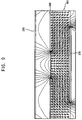
- FIG. 8 is a cross-sectional view illustrating an arrangement of liquid crystal molecules according to a comparative example.
- FIGS. 9 and 10 are cross-sectional views illustrating an arrangement of liquid crystal molecules according to the present invention.
- FIG. 1 is a cross-sectional view illustrating an LCD panel according to an exemplary embodiment of the present invention.
- an LCD panel 100 includes an array substrate 200 , a counter substrate 300 and a liquid crystal layer 400 .
- the array substrate 200 includes an insulation substrate 210 , a thin film transistor (TFT) array 220 and a pixel electrode layer 230 .
- TFT thin film transistor
- the insulation substrate 210 for example, includes a transparent insulating material such as glass.
- the TFT array 220 is layered on the insulation substrate 210 and includes a plurality of TFTs (not shown) and a protection layer (not shown) protecting the TFTs.
- the pixel electrode layer 230 having a uniform thickness is layered on the TFT array 220 .
- the pixel electrode layer 230 for example, includes a transparent conductive material such as indium tin oxide (ITO), indium zinc oxide (IZO), etc.
- ITO indium tin oxide
- IZO indium zinc oxide
- the pixel electrode layer 230 is electrically connected to a drain electrode of each TFT.
- An opening pattern 232 may be formed on the pixel electrode layer 230 to expose the TFT array 220 , such that a viewing angle of the LCD panel 100 may be secured.
- the opening pattern 232 is formed to distort an electric field generated from the pixel electrode layer 230 , thereby generating a fringe field.
- the fringe field controls angles of liquid crystal molecules with respect to the array substrate 200 , so that the viewing angle of the LCD panel 100 may be secured.
- the counter substrate 300 corresponds to a substrate for an LCD panel in the claims.
- a term of “counter substrate” will be used hereinafter for convenience.
- the counter substrate 300 includes an insulation substrate 310 .
- the counter substrate 300 further includes a static electricity discharging layer 320 , a light-blocking layer 330 , a color filter layer 340 , an over-coating layer 350 and a common electrode layer 360 , which are successively layered on the insulation substrate 310 .
- the insulation substrate 310 includes, for example, a transparent insulating material such as glass. The counter substrate 300 will be described in detail as follows.
- FIG. 2 is a plan view illustrating a counter substrate according to an exemplary embodiment of the present invention.
- FIG. 3 is a cross-sectional view taken along a line I-I′ in FIG. 2 .
- the static electricity discharging layer 320 is formed on the insulation substrate 310 .
- the static electricity discharging layer 320 for example, includes a transparent conductive material such as ITO, IZO, etc.
- ITO or IZO is deposited on an entire surface of the insulation substrate 310 to form the static electricity discharging layer 320 .
- the static electricity discharging layer 320 is formed as a floating electrode on the insulation substrate 310 .
- Static electricity is generated at a portion with which the LCD panel 100 externally makes contact. Then, static electric charges are accumulated at the portion when the generated static electricity enters the LCD panel 100 . Even if the LCD panel includes the common electrode layer 360 , the accumulated static electric charges may not be sufficiently discharged through the common electrode layer 360 , so that a spot may be generated when a predetermined pattern is formed on the common electrode layer 360 such as a patterned vertical alignment (PVA) mode.
- PVA patterned vertical alignment
- the static electricity discharging layer 320 is formed as the floating electrode on the entire surface of the insulation substrate 310 , and the accumulated charges are discharged through the static electricity discharging layer 320 , so that a spot due to static electricity may be prevented.
- the static electricity discharging layer 320 may be electrically connected to the common electrode layer 360 to have a stable electric potential.
- the static electricity discharging layer 320 has a predetermined thickness such that light passing through the static electricity discharging layer 320 may have a constructive interference considering optical refractive indexes of the insulation substrate 310 , the light-blocking layer 330 , the color filter layer 340 , the over-coating layer 350 and the common electrode layer 360 .
- the light-blocking layer 330 is formed on the static electricity discharging layer 320 .
- the light-blocking layer 330 includes a plurality of openings that expose the static electricity discharging layer 320 .
- the light-blocking layer 330 blocks light.
- the light-blocking layer 330 includes an organic material such as carbon (C).
- C organic material
- an organic layer including, for example carbon is formed on the static electricity discharging layer 320 , and the organic layer is patterned to form a plurality of openings that exposes the static electricity discharging layer 320 .
- the light-blocking layer 330 may be formed directly on the array substrate 200 .
- the color filter layer 340 is formed on the static electricity discharging layer 320 exposed through the openings.
- the color filter layer 340 includes a red color filter ‘R’, a green color filter ‘G’ and a blue color filter ‘B’.
- a photoresist layer including red colored pigment or a red colored dyes are coated on the insulation substrate 310 having the light-blocking layer formed thereon, and then the photoresist layer is exposed by using a mask having patterns corresponding to the red color filter ‘R’, and developed to form the red color filter ‘R’.
- the green color filter ‘G and the blue color filter ‘B’ may be formed through a same process described above.
- the over-coating layer 350 protects the RGB color filters of the color filter layer 340 , and removes a stepped portion formed by lower layers such as the light-blocking layer 330 , the color filter layer 340 , etc.
- the over-coating layer 350 for example, includes an acryl-group organic layer and/or a polyimide-group organic layer in order to have a flat surface and overcome the stepped portion.
- the common electrode layer 360 is formed on the over-coating layer 350 with a uniform thickness.
- the common electrode layer 360 for example, includes a transparent conductive material such as ITO, IZO, etc.
- the common electrode layer 360 may have an opening pattern 362 formed through the common electrode layer 360 in order to form the fringe field.
- the opening pattern 262 corresponds to the opening pattern 232 of the pixel electrode layer 230 in FIG. 1 .
- the light-blocking layer 330 may be additionally formed on a portion overlapped with the opening pattern 362 to prevent light from passing through the opening pattern 362 .
- the opening pattern 362 of the common electrode layer 360 and the opening pattern 232 of the pixel electrode layer 230 may preferably be alternately formed such that the liquid crystal layer 400 in FIG. 1 may be defined as a plurality of domains.
- the common electrode layer 360 may be formed on the array substrate 200 instead of being formed on the counter substrate 300 .
- an electric field of horizontal direction may be applied to the liquid crystal layer 400 to twist a liquid crystal direction on a plane substantially parallel with an alignment film.
- the array substrate 200 and the counter substrate 300 are combined with each other, so that the LCD panel 100 receives the liquid crystal layer 400 interposed between the array substrate 200 and the counter substrate 300 .
- Liquid crystal molecules of the liquid crystal layer 400 are rearrangeable in accordance with a voltage difference between the pixel electrode layer 230 and the common electrode layer 360 to control an optical transmissivity.
- FIG. 4 is a cross-sectional view illustrating a counter substrate according to another exemplary embodiment of the present invention.
- a counter substrate 500 includes an insulation substrate 510 .
- the counter substrate 500 further includes a light-blocking layer 520 , a static electricity discharging layer 530 , a color filter layer 540 , an over-coating layer 550 and a common electrode layer 560 , which are successively layered on the insulation substrate 510 .
- the insulation substrate 510 for example, includes a transparent conductive material such as glass.
- the light-blocking layer 520 is formed on the insulation substrate 510 .
- the light-blocking layer 520 includes openings that expose the insulation substrate 510 .
- the light-blocking layer 520 blocks light.
- the light-blocking layer 520 for example, includes a metallic material such as chromium (Cr), chromium oxide (CrOx), etc.
- the light-blocking layer 520 may have a double-layered structure of chromium (Cr) and chromium oxide (CrOx) to prevent reflection of an LCD panel including the counter substrate 500 .
- chromium (Cr) layer are layer are formed on the insulation substrate 510 and chromium oxide (CrOx) are formed on the chromium (Cr) layer, then a portion of the chromium (Cr) layer and the chromium oxide (CrOx) are removed to form the openings, so that the light-blocking layer 520 having the openings are completed.
- the static electricity discharging layer 530 is formed on the insulation substrate 510 to cover the light-blocking layer 520 .
- the static electricity discharging layer 530 for example, includes a transparent conductive material such as ITO, IZO, etc. After the light-blocking layer 520 is formed on the insulation substrate 510 , ITO or IZO is deposited on the entire surface of the insulation substrate 510 to form the static electricity discharging layer 530 .
- the static electricity discharging layer 530 is formed as a floating electrode on the entire surface of the insulation substrate 510 , and covers the light-blocking layer 520 .
- the accumulated static electrical charges are discharged through the static electricity discharging layer 530 that is formed as the floating electrode on the entire surface of the insulation substrate 510 .
- the static electricity discharging layer 530 may be electrically connected to the common electrode layer 560 to have a stable electric potential.
- the color filter layer 540 is formed on the static electricity discharging layer 530 .
- Each of the RGB color filters of the color filter layer 540 is formed of the static electricity discharging layer 530 such that each of the RGB color filters is disposed over the openings of the light-blocking layer 520 , and each of the RGB color filters partially overlapped with the light-blocking layer 520 .
- the color filter layer 540 is formed through a substantially same manufacturing process of the color filter layer 340 in FIGS. 1 to 3 . Thus, any further description will be omitted.
- the over-coating layer 550 and the common electrode layer 560 are substantially identical to the over-coating layer 350 and the common electrode layer 360 in FIGS. 1 to 3 , respectively. Thus, any further description will be omitted.
- FIG. 5 is a cross-sectional view illustrating a counter substrate according to still another exemplary embodiment of the present invention.
- a counter substrate 600 includes an insulation substrate 610 .
- the counter substrate 600 further includes a static electricity discharging layer 620 , a light-blocking layer 630 , a color filter layer 640 , an over-coating layer 650 and a common electrode layer 660 , which are successively layered on the insulation substrate 610 .
- the static electricity discharging layer 620 is formed on the insulation substrate 610 .
- the static electricity discharging layer 620 for example, includes a transparent conductive material such as ITO, IZO, etc.
- ITO or IZO is deposited on an entire surface of the insulation substrate 610 to form the static electricity discharging layer 620 .
- the static electricity discharging layer 620 is formed as a floating electrode on the entire surface of the insulation substrate 610 .
- Static electricity is generated at a portion with which the LCD panel 100 externally makes contact.
- the static electricity discharging layer 620 that is formed as the floating electrode on the entire surface of the insulation substrate 610 discharges the static electricity as described in FIGS. 1 to 4 , thereby preventing a spot due to the static electricity.
- the light-blocking layer 630 is formed on the static electricity discharging layer 620 .
- the light-blocking layer 630 includes a plurality of openings that expose the light-blocking layer 630 .
- the light-blocking layer 630 blocks light.
- the light-blocking layer 630 includes a metallic material such as chromium (Cr), chromium oxide (CrOx), etc.
- the light-blocking layer 630 may have a double-layered structure of chromium (Cr) and chromium oxide (CrOx) to prevent reflection of an LCD panel including the counter substrate 600 .
- chromium (Cr) layer are layer are formed on the insulation substrate 510 and chromium oxide (CrOx) are formed on the chromium (Cr) layer, and then a portion of the chromium (Cr) layer and the chromium oxide (CrOx) are removed to form the openings, so that the light-blocking layer 520 having the openings are completed.
- the light-blocking layer 630 may be formed directly on the array substrate in FIG. 1 .
- the light-blocking layer 630 may have a predetermined thickness of chromium (Cr) and/or chromium oxide (CrOx) deposited on the insulation substrate 610 to prevent reflection of the LCD panel including the counter substrate 600 , which will be described in detail with reference to the accompanying drawings.
- Cr chromium
- CrOx chromium oxide
- FIGS. 6 and 7 are cross-sectional views illustrating an optical reflectivity of a light-blocking layer shown in FIG. 5 in accordance with a thickness thereof.
- the light-blocking layer 630 has a double-layered structure of chromium (Cr) and chromium oxide (CrOx). Incident light via a transparent conductive material such as ITO, IZO, etc. is reflected or transmitted in accordance with the incident angle of light.
- Cr chromium
- CrOx chromium oxide
- a first thickness of chromium (Cr) and a second thickness of chromium oxide (CrOx) of the light-blocking layer 630 may be controlled to increase a canceled amount of light, thereby reducing an optical reflectivity of the light-blocking layer 630 .
- a ratio of the first thickness with respect to the second thickness may not be controlled.
- the ratio may be controlled.
- the color filter layer 640 is formed on the static electricity discharging layer 620 .
- Each of the RGB color filters of the color filter layer 640 is partially overlapped with the light-blocking layer 630 .
- the color filter layer 640 is substantially identical to the color filter layer 340 in FIGS. 1 to 3 except for the color filter layer 640 being partially overlapped with the light-blocking layer 630 . Thus, any further description will be omitted.
- the over-coating layer 650 and the common electrode layer 660 are substantially identical to the over-coating layer 350 and the common electrode layer 360 , respectively, as shown in FIGS. 1 to 3 . Thus, any further description will be omitted.
- FIG. 8 is a cross-sectional view illustrating an arrangement of liquid crystal molecules according to a comparative example.
- liquid crystal molecules are rearranged by an electric field generated between a pixel electrode layer 23 formed on an array substrate and a common electrode layer 36 formed on a counter substrate to control an optical transmissivity.
- a common voltage of about 5V is applied to the common electrode layer 36
- a pixel voltage of about 0V to about 10V is applied to the pixel electrode layer 23
- vertically aligned liquid crystal molecules are rearranged by a distorted electric field that is generated in accordance with patterns of the common electrode layer 36 and the pixel electrode layer 23 .
- An optical transmissivity of light passing through a liquid crystal layer may be controlled.
- FIGS. 9 and 10 are cross-sectional views illustrating an arrangement of liquid crystal molecules according to the present invention.
- FIG. 9 a simulated result of an arrangement of liquid crystal molecules is shown when a static electricity discharging layer according to the present invention is electrically floated.
- FIG. 9 illustrates a simulated result when an anti-static treatment on a polarizing film of an LCD panel having a PVA mode is omitted, and a static electricity discharging layer 320 is formed.
- FIG. 10 a simulated result of an arrangement of liquid crystal molecules is shown when a predetermined electric filed is applied to a static electricity discharging layer according to the present invention.
- FIG. 10 illustrates a simulated result when an anti-static treatment on a polarizing film of an LCD panel having a PVA mode is omitted, and a static electricity discharging layer 320 is formed.
- a same common voltage and a same pixel voltage as in FIG. 8 are applied to the common electrode layer 360 and the pixel electrode layer 230 , respectively.
- the LCD panel has substantially same arrangement of liquid crystal molecules as the LCD panel having an anti-static polarizing film shown in FIG. 8 .
- an anti-static treatment process for preventing a spot due to static electricity may be omitted, so that manufacturing cost of an LCD panel may be reduced and an optical transmissivity of the LCD panel may be improved.
- the LCD panel may have an equivalent viewing angle to an LCD panel manufactured through an anti-static treatment process.
- the present invention is applied to a PVA mode that a predetermined pattern is formed on a common electrode of a counter substrate facing an array substrate.
- the present invention is not limited to the PVA mode.
- the present invention may be applied to an IPS mode of which a common electrode is not formed on a counter substrate.
- the present invention is applied to a color filter substrate on which a color filter layer is formed.
- the present invention is not limited to the color filter substrate.
- the present invention may be applied to an array substrate on which a color filter layer and a light-blocking layer are formed.
- the static electricity when static electricity generated by making contact with an outside flows into an LCD panel, the static electricity may be discharged by a floating electrode formed on an entire surface of the LCD panel, thereby preventing a spot due to static electricity.
- an anti-static treatment process for discharging static electricity that flows into the LCD panel may be omitted, so that manufacturing cost of the LCD panel may be reduced.
- the anti-static treatment process is omitted, so that loss of an optical transmissivity of the LCD panel may be prevented by omitting a use of conductive metal for the anti-static treatment process.
Landscapes
- Physics & Mathematics (AREA)
- Nonlinear Science (AREA)
- Mathematical Physics (AREA)
- Chemical & Material Sciences (AREA)
- Crystallography & Structural Chemistry (AREA)
- General Physics & Mathematics (AREA)
- Optics & Photonics (AREA)
- Engineering & Computer Science (AREA)
- General Engineering & Computer Science (AREA)
- Mechanical Engineering (AREA)
- Liquid Crystal (AREA)
Abstract
Description
Claims (20)
Applications Claiming Priority (3)
| Application Number | Priority Date | Filing Date | Title |
|---|---|---|---|
| KR1020050029217A KR20060107169A (en) | 2005-04-08 | 2005-04-08 | Substrate for liquid crystal display panel, manufacturing method thereof and liquid crystal display panel having same |
| KR10-2005-0029217 | 2005-04-08 | ||
| KR2005-29217 | 2005-04-08 |
Publications (2)
| Publication Number | Publication Date |
|---|---|
| US20060227257A1 US20060227257A1 (en) | 2006-10-12 |
| US7656466B2 true US7656466B2 (en) | 2010-02-02 |
Family
ID=37082812
Family Applications (1)
| Application Number | Title | Priority Date | Filing Date |
|---|---|---|---|
| US11/304,860 Expired - Fee Related US7656466B2 (en) | 2005-04-08 | 2005-12-14 | Substrate for a liquid crystal display panel, method of manufacturing the same and liquid crystal display device having the same |
Country Status (2)
| Country | Link |
|---|---|
| US (1) | US7656466B2 (en) |
| KR (1) | KR20060107169A (en) |
Cited By (1)
| Publication number | Priority date | Publication date | Assignee | Title |
|---|---|---|---|---|
| CN105549258A (en) * | 2016-02-18 | 2016-05-04 | 武汉华星光电技术有限公司 | Color film substrate and production method thereof |
Families Citing this family (6)
| Publication number | Priority date | Publication date | Assignee | Title |
|---|---|---|---|---|
| KR101589753B1 (en) * | 2009-10-08 | 2016-01-28 | 엘지디스플레이 주식회사 | Display device |
| KR101960532B1 (en) * | 2012-04-19 | 2019-03-20 | 엘지디스플레이 주식회사 | Electrostatic capacity type touch screen panel for display device and method of manufacturing the same |
| CN104216596B (en) * | 2014-09-29 | 2017-09-22 | 上海天马微电子有限公司 | Embedded touch display device and manufacturing method thereof |
| CN108594516A (en) * | 2018-05-03 | 2018-09-28 | 京东方科技集团股份有限公司 | Display base plate and preparation method thereof, display panel, display device |
| KR102808070B1 (en) * | 2020-12-23 | 2025-05-14 | 엘지디스플레이 주식회사 | Liquid Crystal Display Device |
| CN113325625B (en) * | 2021-06-24 | 2022-07-29 | 业成科技(成都)有限公司 | Preparation method of display panel |
Citations (6)
| Publication number | Priority date | Publication date | Assignee | Title |
|---|---|---|---|---|
| US4432610A (en) * | 1980-02-22 | 1984-02-21 | Tokyo Shibaura Denki Kabushiki Kaisha | Liquid crystal display device |
| US20020008824A1 (en) * | 1998-08-26 | 2002-01-24 | Ki Sup Son | In-plane switching mode liquid crystal display device capable of shielding against interferences |
| US20030020845A1 (en) * | 2001-07-10 | 2003-01-30 | Hyun-Kyu Lee | Protection circuit and method from electrostatic discharge of TFT-LCD |
| US6525786B1 (en) * | 1999-11-19 | 2003-02-25 | Nec Corporation | Transverse electric liquid crystal display device |
| US6642972B2 (en) * | 2000-07-13 | 2003-11-04 | Lg. Philips Lcd Co., Ltd. | Array substrate for a liquid crystal display and method for fabricating thereof with insulating stack made from TFT layers between crossed conductors |
| US6657695B1 (en) * | 1999-06-30 | 2003-12-02 | Samsung Electronics Co., Ltd. | Liquid crystal display wherein pixel electrode having openings and protrusions in the same substrate |
-
2005
- 2005-04-08 KR KR1020050029217A patent/KR20060107169A/en not_active Ceased
- 2005-12-14 US US11/304,860 patent/US7656466B2/en not_active Expired - Fee Related
Patent Citations (7)
| Publication number | Priority date | Publication date | Assignee | Title |
|---|---|---|---|---|
| US4432610A (en) * | 1980-02-22 | 1984-02-21 | Tokyo Shibaura Denki Kabushiki Kaisha | Liquid crystal display device |
| US20020008824A1 (en) * | 1998-08-26 | 2002-01-24 | Ki Sup Son | In-plane switching mode liquid crystal display device capable of shielding against interferences |
| US6400435B2 (en) * | 1998-08-26 | 2002-06-04 | Lg. Philips Lcd Co., Ltd. | In-plane switching mode liquid crystal display device capable of shielding against interferences |
| US6657695B1 (en) * | 1999-06-30 | 2003-12-02 | Samsung Electronics Co., Ltd. | Liquid crystal display wherein pixel electrode having openings and protrusions in the same substrate |
| US6525786B1 (en) * | 1999-11-19 | 2003-02-25 | Nec Corporation | Transverse electric liquid crystal display device |
| US6642972B2 (en) * | 2000-07-13 | 2003-11-04 | Lg. Philips Lcd Co., Ltd. | Array substrate for a liquid crystal display and method for fabricating thereof with insulating stack made from TFT layers between crossed conductors |
| US20030020845A1 (en) * | 2001-07-10 | 2003-01-30 | Hyun-Kyu Lee | Protection circuit and method from electrostatic discharge of TFT-LCD |
Cited By (3)
| Publication number | Priority date | Publication date | Assignee | Title |
|---|---|---|---|---|
| CN105549258A (en) * | 2016-02-18 | 2016-05-04 | 武汉华星光电技术有限公司 | Color film substrate and production method thereof |
| CN105549258B (en) * | 2016-02-18 | 2019-02-01 | 武汉华星光电技术有限公司 | Color filter substrate and manufacturing method thereof |
| US10359548B2 (en) | 2016-02-18 | 2019-07-23 | Wuhan China Star Optoelectronics Technolog Co., Ltd | Color filter substrate and method for manufacturing the same |
Also Published As
| Publication number | Publication date |
|---|---|
| KR20060107169A (en) | 2006-10-13 |
| US20060227257A1 (en) | 2006-10-12 |
Similar Documents
| Publication | Publication Date | Title |
|---|---|---|
| US12164200B2 (en) | Liquid crystal display panel | |
| US7557886B2 (en) | Liquid crystal display device and method of fabricating the same | |
| US7633595B2 (en) | Liquid crystal display panel having dummy color filter and fabricating method thereof | |
| US7388639B2 (en) | In-plane switching mode liquid crystal display device having multi-domains | |
| US9176339B2 (en) | Liquid crystal display device | |
| KR100747357B1 (en) | Liquid crystal display device and method of fabricating the same | |
| US6879353B2 (en) | Array substrate for IPS mode liquid crystal display device | |
| US20100220253A1 (en) | Liquid crystal display panel | |
| KR100817366B1 (en) | Color filter substrate for liquid crystal display device and manufacturing method thereof | |
| US20050099569A1 (en) | Substrate for in-plane switching mode liquid crystal display device and method for fabricating the same | |
| US20050195353A1 (en) | Liquid crystal display apparatus and method of manufacturing the same | |
| KR100734461B1 (en) | Liquid crystal display device | |
| US8054420B2 (en) | Liquid crystal display device and method of fabricating the same | |
| KR101802935B1 (en) | In plane switching mode liquid crystal display device and method of fabricating thereof | |
| US7656466B2 (en) | Substrate for a liquid crystal display panel, method of manufacturing the same and liquid crystal display device having the same | |
| US7626658B2 (en) | Liquid crystal display device with color filter covering extended black matrix at a seal pattern region at periphery of the display active region | |
| US6900862B2 (en) | In-plane switching mode liquid crystal display device | |
| JP2008241959A (en) | Liquid crystal display | |
| CN100412670C (en) | Pixel structure and liquid crystal display panel | |
| JP2009145524A (en) | Liquid crystal device and electronic device | |
| JP2003107525A (en) | Active matrix substrate |
Legal Events
| Date | Code | Title | Description |
|---|---|---|---|
| AS | Assignment |
Owner name: SAMSUNG ELECTRONICS CO., LTD.,KOREA, REPUBLIC OF Free format text: ASSIGNMENT OF ASSIGNORS INTEREST;ASSIGNORS:DO, HEE-WOOK;LEE, CHANG-HUN;CHANG, HAK-SUN;AND OTHERS;REEL/FRAME:017330/0484 Effective date: 20051121 Owner name: SAMSUNG ELECTRONICS CO., LTD., KOREA, REPUBLIC OF Free format text: ASSIGNMENT OF ASSIGNORS INTEREST;ASSIGNORS:DO, HEE-WOOK;LEE, CHANG-HUN;CHANG, HAK-SUN;AND OTHERS;REEL/FRAME:017330/0484 Effective date: 20051121 |
|
| FEPP | Fee payment procedure |
Free format text: PAYOR NUMBER ASSIGNED (ORIGINAL EVENT CODE: ASPN); ENTITY STATUS OF PATENT OWNER: LARGE ENTITY |
|
| AS | Assignment |
Owner name: SAMSUNG DISPLAY CO., LTD., KOREA, REPUBLIC OF Free format text: ASSIGNMENT OF ASSIGNORS INTEREST;ASSIGNOR:SAMSUNG ELECTRONICS CO., LTD.;REEL/FRAME:029008/0145 Effective date: 20120904 |
|
| FEPP | Fee payment procedure |
Free format text: PAYER NUMBER DE-ASSIGNED (ORIGINAL EVENT CODE: RMPN); ENTITY STATUS OF PATENT OWNER: LARGE ENTITY Free format text: PAYOR NUMBER ASSIGNED (ORIGINAL EVENT CODE: ASPN); ENTITY STATUS OF PATENT OWNER: LARGE ENTITY |
|
| FPAY | Fee payment |
Year of fee payment: 4 |
|
| FEPP | Fee payment procedure |
Free format text: MAINTENANCE FEE REMINDER MAILED (ORIGINAL EVENT CODE: REM.) |
|
| LAPS | Lapse for failure to pay maintenance fees |
Free format text: PATENT EXPIRED FOR FAILURE TO PAY MAINTENANCE FEES (ORIGINAL EVENT CODE: EXP.) |
|
| STCH | Information on status: patent discontinuation |
Free format text: PATENT EXPIRED DUE TO NONPAYMENT OF MAINTENANCE FEES UNDER 37 CFR 1.362 |
|
| FP | Lapsed due to failure to pay maintenance fee |
Effective date: 20180202 |