US7633179B2 - Passenger detection apparatus for detecting breakage on shield line without being affected by peripheral shield cables - Google Patents
Passenger detection apparatus for detecting breakage on shield line without being affected by peripheral shield cables Download PDFInfo
- Publication number
- US7633179B2 US7633179B2 US11/902,953 US90295307A US7633179B2 US 7633179 B2 US7633179 B2 US 7633179B2 US 90295307 A US90295307 A US 90295307A US 7633179 B2 US7633179 B2 US 7633179B2
- Authority
- US
- United States
- Prior art keywords
- shield
- signal
- capacitance
- measurement
- accordance
- Prior art date
- Legal status (The legal status is an assumption and is not a legal conclusion. Google has not performed a legal analysis and makes no representation as to the accuracy of the status listed.)
- Expired - Fee Related, expires
Links
Images


Classifications
-
- B—PERFORMING OPERATIONS; TRANSPORTING
- B60—VEHICLES IN GENERAL
- B60R—VEHICLES, VEHICLE FITTINGS, OR VEHICLE PARTS, NOT OTHERWISE PROVIDED FOR
- B60R21/00—Arrangements or fittings on vehicles for protecting or preventing injuries to occupants or pedestrians in case of accidents or other traffic risks
- B60R21/01—Electrical circuits for triggering passive safety arrangements, e.g. airbags, safety belt tighteners, in case of vehicle accidents or impending vehicle accidents
- B60R21/015—Electrical circuits for triggering passive safety arrangements, e.g. airbags, safety belt tighteners, in case of vehicle accidents or impending vehicle accidents including means for detecting the presence or position of passengers, passenger seats or child seats, and the related safety parameters therefor, e.g. speed or timing of airbag inflation in relation to occupant position or seat belt use
- B60R21/01512—Passenger detection systems
- B60R21/0153—Passenger detection systems using field detection presence sensors
- B60R21/01532—Passenger detection systems using field detection presence sensors using electric or capacitive field sensors
Definitions
- the present invention relates to a passenger (state) detection apparatus for detecting a seated state of a passenger seated in a vehicle, in particular, a passenger detection apparatus which can detect a breakage on a shield line for connecting a detector main body (i.e., control box) and a sensor.
- a detector main body i.e., control box
- a passenger detection apparatus for detecting such a seated state has been developed (see Patent Document 1).
- a sensor for detection is attached to a target seat in a vehicle, and a high-frequency low voltage is applied to this sensor.
- the seated state of a passenger is determined by using a phenomenon such that the current, which flows through the sensor, changes depending on the state of the passenger on the target seat.
- a high-frequency low voltage is used, and thus a shield line is employed for connecting the control box to the sensor. If breaking of the shield line occurs, passenger (state) detection may not be accurately performed. Therefore, a technique for detecting a breakage of the shield line is required. However, in a state in which a plurality of shield cables are crowdedly bundled, detection of a breakage in the shield line may not be accurately performed.
- an object of the present invention is to provide a passenger detection apparatus for reliably detecting a breakage of a shield line without being affected by peripheral shield cables.
- the present invention provides a passenger detection apparatus comprising:
- each shield cable has a shield and a core wire, wherein one end the core wire is connected to the corresponding one of the sensors;
- a measurement signal output device for outputting a measurement AC signal
- a current detection device for detecting a current output from the measurement signal output device
- a canceling signal output device for outputting a capacitance canceling AC signal, which has the same phase and the same level as those of the measurement AC signal;
- a first selection device for selectively applying one of the measurement AC signal and a DC voltage to the other end of each shield cable
- a second selection device for selectively applying one of the capacitance canceling AC signal and a second signal, which has a different waveform from that of the measurement AC signal, to the shield of each shield cable.
- the passenger detection apparatus may further comprise:
- control device for controlling the first selection device and the second selection device, wherein the control device performs:
- the passenger detection apparatus may further comprise:
- an adjustment device for adjusting the level of the measurement AC signal and the capacitance canceling AC signal.
- the second selection device includes:
- a switch device for switching on or off the capacitance canceling AC signal in accordance with the control of the control device
- an amplifier for amplifying the capacitance canceling AC signal when the switch device is on, so as to apply the amplified signal to the shield of the relevant shield cable, and amplifying the second signal when the switch device is off, so as to apply the amplified signal to the above shield.
- the second selection device includes:
- a transistor for grounding an input terminal of the amplifier in accordance with the control of the control device.
- the second selection device includes:
- a transistor for grounding a part between the resistor and the relevant shield cable in accordance with the control of the control device.
- the second selection device includes:
- a transistor for connecting an input terminal of the amplifier to a positive voltage terminal in accordance with the control of the control device.
- the second selection device includes:
- a transistor for connecting a part between the resistor and the relevant shield cable to a positive voltage terminal in accordance with the control of the control device.
- the passenger detection apparatus may further comprise:
- an AC signal output device for outputting an AC signal, which has a different waveform from that of the measurement AC signal and functions as the second signal.
- the second signal is a DC voltage.
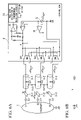
- FIG. 1A is a circuit diagram showing the structure of the passenger detection apparatus as a first embodiment in accordance with the present invention.
- FIG. 1B shows an equivalent circuit of the capacitance observed from the point A in FIG. 1A .
- FIG. 2 is a circuit diagram for explaining the capacitance C 2 in the passenger detection apparatus
- FIG. 3A is a circuit diagram for explaining the operation when the shield cables are arranged distant from each other, and there is no breakage with respect to the shield cables in the passenger detection apparatus.
- FIG. 3B shows an equivalent circuit of the capacitance observed from the point A in FIG. 3A .
- FIG. 4A is a circuit diagram for explaining the operation when the shield cables are arranged distant from each other, and a wiring line connected to a shield cable has a breakage in the passenger detection apparatus.
- FIG. 4B shows an equivalent circuit of the capacitance observed from the point A in FIG. 4A .
- FIG. 5A is also a circuit diagram for explaining the operation when the shield cables are arranged distant from each other, and a wiring line connected to a shield cable has a breakage in the passenger detection apparatus.
- FIG. 5B shows an equivalent circuit of the capacitance observed from the point A in FIG. 5A .
- FIG. 6A is a circuit diagram for explaining the operation when the shield cables are arranged close to each other, and there is no breakage with respect to the shield cables in the passenger detection apparatus.
- FIG. 6B shows an equivalent circuit of the capacitance observed from the point A in FIG. 6A .
- FIG. 7A is also a circuit diagram for explaining the operation when the shield cables are arranged close to each other, and there is no breakage with respect to the shield cables in the passenger detection apparatus.
- FIG. 7B shows an equivalent circuit of the capacitance observed from the point A in FIG. 7A .
- FIG. 8A is a circuit diagram for explaining the operation when the shield cables are arranged close to each other, and a wiring line connected to a shield cable has a breakage in the passenger detection apparatus.
- FIG. 8B shows an equivalent circuit of the capacitance observed from the point A in FIG. 8A .
- FIG. 9A is also a circuit diagram for explaining the operation when the shield cables are arranged close to each other, and a wiring line connected to a shield cable has a breakage in the passenger detection apparatus.
- FIG. 9B shows an equivalent circuit of the capacitance observed from the point A in FIG. 9A .
- FIG. 10A is a circuit diagram for explaining the operation when the shield cables are arranged distant from each other, and one of the shield cables itself has a breakage.
- FIG. 10B shows an equivalent circuit of the capacitance observed from the point A in FIG. 10A .
- FIG. 11A is also a circuit diagram for explaining the operation when the shield cables are arranged distant from each other, and one of the shield cables itself has a breakage.
- FIG. 11B shows an equivalent circuit of the capacitance observed from the point A in FIG. 11A .
- FIG. 12A is a circuit diagram for explaining the operation when the shield cables are arranged close to each other, and one of the shield cables itself has a breakage.
- FIG. 12B shows an equivalent circuit of the capacitance observed from the point A in FIG. 12A .
- FIG. 13A is also a circuit diagram for explaining the operation when the shield cables are arranged close to each other, and one of the shield cables itself has a breakage.
- FIG. 13B shows an equivalent circuit of the capacitance observed from the point A in FIG. 13A .
- FIG. 14 is a circuit diagram showing the structure of the passenger detection apparatus as a second embodiment in accordance with the present invention.
- FIG. 15 is a circuit diagram showing the structure of the passenger detection apparatus as a third embodiment in accordance with the present invention.
- FIG. 16 is a circuit diagram showing the structure of the passenger detection apparatus as a fourth embodiment in accordance with the present invention.
- FIG. 17 is a circuit diagram showing the structure of the passenger detection apparatus as a fifth embodiment in accordance with the present invention.
- FIG. 18 is a circuit diagram showing the structure of the passenger detection apparatus as a sixth embodiment in accordance with the present invention.
- FIG. 19 is a circuit diagram showing the structure of the passenger detection apparatus as a seventh embodiment in accordance with the present invention.
- FIG. 20 is a circuit diagram showing the structure of the passenger detection apparatus as an eighth embodiment in accordance with the present invention.
- FIG. 1A is a circuit diagram showing the structure of the passenger detection apparatus as the first embodiment.
- reference numeral 1 indicates a passenger sitting on a seat in a vehicle.
- the passenger 1 can be treated as a conductor.
- Reference numerals 2 - 1 to 2 - 3 indicate sensors attached to the seat at regular intervals. Each sensor may be made by using a conductive cloth, a material into which thin metal wires are woven, a metal plate, or the like.
- Reference symbol CL 1 indicates a capacitance between the sensor 2 - 1 and the passenger 1
- reference symbol CL 2 indicates a capacitance between the sensor 2 - 2 and the passenger 1
- reference symbol CL 3 indicates a capacitance between the sensor 2 - 3 and the passenger 1
- reference symbol Cg indicates a capacitance between the passenger 1 and the earth (i.e., the vehicle body).
- Reference numerals 3 - 1 to 3 - 3 respectively indicate shield cables for connecting the sensors 2 - 1 to 2 - 3 to a control box 4 .
- the control box 4 is installed inside the seat or in a dashboard, or the like, and outputs a detection voltage for detecting the state of the passenger 1 based on a current, which flows through the core wire of each shield cable.
- reference numeral 5 indicates an AC (alternating current) oscillator for outputting a sine-wave AC signal of a high-frequency low voltage
- reference numeral 6 indicates an operation amplifier for amplifying the signal output from the AC oscillator 5
- reference numeral 7 indicates a current detection resistor for detecting the current, which flows through each core wire of the shield cables 3 - 1 to 3 - 3 .
- the inverse input terminal of the operation amplifier 6 is connected to the other terminal (“one terminal” will appear later for convenience of explanation) (see point A) of the current detection resistor 7 , thereby preventing the voltage at the point A from varying due to a voltage drop through the current detection resistor 7 .
- the signal output from the operation amplifier 6 is output as an AC signal for relevant measurement.
- Reference numeral 8 indicates an operation amplifier for amplifying the voltage between both ends of the current detection resistor 7 .
- Reference numeral 9 indicates an input resistor for inputting the voltage at point A into the non-inverse input terminal of the operation amplifier 8 .
- Reference numeral 10 indicates a resistor for applying a positive bias to the above non-inverse input terminal of the operation amplifier 8 .
- Reference numeral 11 indicates an input resistor for inputting the voltage at one terminal of the current detection resistor 7 into the inverse input terminal of the operation amplifier 8 .
- Reference numeral 12 indicates a resistor for feeding back the signal output from the operation amplifier 8 to the inverse input terminal thereof.
- Reference numeral 14 indicates a full-wave rectifying or synchronous detection circuit for performing full-wave rectification or synchronous detection of the signal output from the operation amplifier 8 . The result of this performance is output from the circuit 14 as a detection voltage which indicates the state of the passenger 1 .
- Reference numeral 16 indicates an operation amplifier which functions as a voltage follower for amplifying the signal output from the AC oscillator 5 .
- the signal output from the operation amplifier 16 is used as a capacitance canceling AC signal.
- Reference symbols SW 1 to SW 3 indicate semiconductor switches.
- the common terminal of the switch SW 1 is connected to the core wire of the shield cable 3 - 1 , and the first and second contacts of the switch SW 1 are respectively connected to the other terminal (at point A) of the current detection resistor 7 and a DC (direct current) voltage DC.
- the common terminal of the switch SW 2 is connected to the core wire of the shield cable 3 - 2 , and the first and second contacts of the switch SW 2 are respectively connected to the other terminal (at point A) of the current detection resistor 7 and the DC voltage DC.
- the common terminal of the switch SW 3 is connected to the core wire of the shield cable 3 - 3 , and the first and second contacts of the switch SW 3 are respectively connected to the other terminal (at point A) of the current detection resistor 7 and
- Reference symbols SW 1 S to SW 3 S also indicate semiconductor switches.
- the common terminal of the switch SW 1 S is connected to the shield of the shield cable 3 - 1 , and the first and second contacts of the switch SW 1 are respectively connected to the output terminal of the operation amplifier 16 and the DC voltage DC.
- the common terminal of the switch SW 2 S is connected to the shield of the shield cable 3 - 2 , and the first and second contacts of the switch SW 2 S are respectively connected to the output terminal of the operation amplifier 16 and the DC voltage DC.
- the common terminal of the switch SW 3 S is connected to the shield of the shield cable 3 - 3 , and the first and second contacts of the switch SW 3 S are respectively connected to the output terminal of the operation amplifier 16 and the DC voltage DC.
- Switching of the above switches SW 1 to SW 3 and SW 1 S to SW 3 S is performed and controlled by a control device (not shown); however, it may be performed manually.
- the common terminal of the switch SW 2 is connected to the first contact (thereof), the common terminals of the switches SW 1 and SW 3 are each connected to the second contact (of each of them), and the common terminals of the switches SW 1 S to SW 3 S are each connected to the first contact (of each of them).
- the above connection state is called a “first connection state”.
- the capacitance CL 2 is connected via the core wire of the shield cable 3 - 2 to the point A.
- the capacitances CL 1 , CL 3 , and Cg are connected via the passenger 1 .
- the terminals opposite to the passenger 1 are respectively connected via the core wires of the shield cables 3 - 1 and 3 - 3 and also via switches SW 1 S and SW 3 S to the DC voltage DC.
- the terminal opposite to the passenger 1 is grounded.
- C 2 is the total capacitance of the above capacitances CL 2 , CL 1 , CL 3 , and Cg.
- a capacitance Cs 2 is present between the core wire and the shield of the shield cable 3 - 2
- a capacitance Csg 2 is present between this shield and the ground (or earth).
- the shield of the shield cable 3 - 2 is connected to the output terminal of the operation amplifier 16 via the switch SW 2 S, so that the shield and the core wire have the same electric potential. Therefore, no current flows through the capacitance Cs 2 , and thus the relevant measurement is not affected by the capacitance Cs 2 .
- the common terminal of the switch SW 2 is connected to the first contact (thereof), the common terminals of the switches SW 1 and SW 3 are each connected to the second contact (of each of them), the common terminal of the switch SW 2 S is connected to the second contact (thereof), and the common terminals of the switches SW 1 S and SW 3 S are each connected to the first contact (of each of them).
- This connection state is called a “second connection state”.
- the shield of the shield cable 3 - 2 is connected via the switch SW 2 S to the DC voltage DC. Therefore, an AC current flows through the capacitance Cs 2 , and thus the relevant measurement is affected by the capacitance Cs 2 .
- the equivalent circuit of the capacitance observed from the point A is formed by connecting the capacitance C 2 and “a capacitance of the serial circuit of the capacitances Cs 2 and Csg 2 ” in parallel (see FIG. 4B ), and thus the capacitance observed from the point A is equal to “C 2 +(Cs 2 ⁇ Csg 2 )/(Cs 2 +Csg 2 )”.
- the measured capacitance i.e., the detection voltage output from the full-wave rectifying or synchronous detection circuit 4
- the difference corresponds to the capacitance Cs 2
- the capacitance observed from the point A is approximately equal to that observed when there is no breakage (i.e., C 2 ) (see FIG. 8B ).
- the measured capacitance (corresponding to the detection voltage output from the full-wave rectifying or synchronous detection circuit 4 ) has a different value between the first and second connection states of the switches SW 1 to SW 3 and SW 1 S to SW 3 S (the difference corresponds to the capacitance Cs 2 ).
- the difference corresponds to the capacitance Cs 2 .
- a shield breakage occurs at the center of the shield cable 3 - 2 (see FIG. 10A ).
- a shield part toward the sensor 2 - 2 is called a shield 3 - 2 a
- the remaining shield part toward the switch SW 2 S is called a shield 3 - 2 b .
- the capacitance between the shield 3 - 2 a and the corresponding core wire is called Cs 2 a
- the capacitance between the shield 3 - 2 b and the corresponding core wire is called Cs 2 b
- the capacitance between the shield 3 - 2 a and the ground is called Csg 2 a
- the capacitance between the shield 3 - 2 b and the ground is called Csg 2 b.
- the measured value has a difference (corresponding to the capacitance Cs 2 b ) between the first and second connection states of the switches SW 1 to SW 3 and SW 1 S to SW 3 S. Also as described above, when there is no breakage (see FIGS. 1A to 2B ), the difference between the measured values in both connection states corresponds to the capacitance Cs 2 . Therefore, in accordance with the difference between the former difference corresponding to Cs 2 b and the latter difference corresponding to Cs 2 , it is possible to determine whether there is a breakage of a shield cable.
- the length B can be computed by using the measured capacitance difference Cs 2 b , and thus it is possible to determine a spot where the breakage has occurred.
- the AC signal is applied via a capacitance Cs 21 a between the shield of the shield cable 3 - 1 and the shield 3 - 2 a and a capacitance Cs 23 a between the shield of the shield cable 3 - 3 and the shield 3 - 2 a .
- the shield 3 - 2 a and the core wire of the shield cable 3 - 2 have the same electric potential, so that no current flows through the capacitance Cs 2 a . Therefore, the capacitance Cs 2 a does not affect the relevant measurement.
- the capacitance observed from the point A is shown by FIG. 12B , that is, C 2 .
- the measured value has a difference corresponding to the capacitance Cs 2 b between the first and second connection states of the switches SW 1 to SW 3 and SW 1 S to SW 3 S, similar to the case shown by FIGS. 10A to 11B . Therefore, based on the difference from the measured-value difference when no breakage occurs, it is possible to determine whether a shield breakage has occurred.
- the length B of the shield 3 - 2 b can be obtained based on the measured capacitance Cs 2 b.
- the first embodiment has been explained in detail.
- the above explanation employs only a case in which an AC signal for measurement is applied to the core wire of the shield cable 3 - 2 .
- an AC signal for measurement is of course also applied to each of the shield cable 3 - 1 and 3 - 3 in accordance with a similar method, so as to measure a target capacitance.
- C 1 and C 3 (respectively corresponding to the shield cable 3 - 1 and 3 - 3 ) each function as a total capacitance, similar to C 2 in the above embodiment.
- the capacitances C 1 , C 2 , and C 3 can be measured, and the state of the passenger 1 can be detected based on the results of the measurement. Additionally, when a breakage occurs in a wiring line connected to a relevant shield or on the shield itself, the breakage can be detected regardless of whether the shield cables are arranged distant from each other or close to each other. Furthermore, when a shield breakage occurs, the spot of the breakage can also be detected.
- FIGS. 14 to 20 are circuit diagrams, which respectively show second to eighth embodiments of the present invention.
- DC indicates a DC voltage having the same electric potential as the middle point voltage of the signal output from the AC oscillator 5
- VDD indicates a source voltage for the operation amplifiers and a multiplexer 25 (VDD is not shown in some of the figures).
- the embodiment shown in FIG. 14 has a distinctive feature of providing an amplitude control circuit 21 for switching the amplitude of a sine-wave AC signal.
- an amplitude control circuit 21 for switching the amplitude of a sine-wave AC signal.
- the switch SW 1 is set to the AC output side, while the switches SW 2 and SW 3 are each set to the DC output side. That is, the DC voltage DC is applied to the sensors 2 - 2 and 2 - 3 by setting the switches SW 2 and SW 3 to the DC output side, so as to positively generate a capacitance element between the sensor 2 - 1 and the passenger 1 .
- the switches SW 1 S, SW 2 S, and SW 3 S in the multiplexer 25 are each set to the AC output side (i.e., toward the operation amplifier 16 .
- the above connection state is called the first connection state.
- this connection state is called the second connection state.
- the capacitance Cs 1 between the core wire and the shield of the shield cable 3 - 1 is added to the capacitance C 1 in the measurement. Therefore, “no breakage” can be determined in accordance with the difference Cs 1 between the first and second connection states (see FIGS. 1A , 1 B, 3 A, 3 B, and 6 A to 7 B).
- the first and second connection states have an identical peripheral state with respect to the shield cable 3 - 1 . Therefore, if the shield cable 3 - 1 has a breakage, the first and second connection states have the same measured value, and thus the difference thereof is zero (see FIGS. 4A to 5B and 8 A to 9 B).
- the relevant switch SW 2 or SW 3 is turned to the DC output side so as to measure the capacitance between the core wire and the shield of the switch SW 2 or SW 3 , and the presence/absence of breakage is determined based on the measured capacitance.
- FIG. 15 shows a structure in which the switches SW 1 S to SW 3 S in the multiplexer 25 in FIG. 14 are each modified to a two-point type, and operation amplifiers 22 - 1 to 22 - 3 and pull-up resistors R 1 to R 3 for a DC voltage are provided behind the switches.
- the procedure for shield breakage determination is similar to that for the structure in FIG. 14 .
- the corresponding switch SW 1 S, SW 2 S, or SW 3 S is turned on.
- the relevant switch is turned off, so that the DC voltage is applied to the positive input terminal of the relevant operation amplifier 22 - 1 , 22 - 2 , or 22 - 3 via the corresponding resistor R 1 , R 2 , or R 3 , so that the relevant shield has a DC electric potential.
- the middle point voltage DC of the signal output from the AC oscillator 5 is used as the DC voltage applied to the relevant shield.
- the detection apparatus detects a change in the capacitance element by referring to a variation in the AC element of the current which flows through the current detection resistor. Therefore, the DC electric potential applied to the shield is not necessarily the middle-point electric potential of the signal output from the AC oscillator 5 , and may be the GND electric potential, or the source voltage VDD of the operation amplifiers may be used.
- the absolutely necessary condition is that a current flows through a capacitance element (or the current detection resistor 7 ).
- the voltage applied to the relevant shield is not necessarily a DC voltage, and an AC signal having a different waveform (i.e., different level) from the signal output from the operation amplifier 6 may be used. That is, any signal can be used if the signal-level difference between this signal and the signal output from the operation amplifier 6 temporally varies, that is, if a displacement current flows through a relevant capacitance element due to the signal.
- FIG. 16 shows an example in which a voltage of the GND level is used as a DC voltage to be output to the shield cables 3 - 1 to 3 - 3 .
- the procedure of determining whether there is a shield breakage is the same as that performed for the structure of FIG. 14 .
- transistors Q- 1 to Q- 3 are provided, which correspond to the switches SW 1 S, SW 2 S, and SW 3 S in the multiplexer 25 in FIG. 15 .
- the base signal of the relevant transistor Q- 1 , Q- 2 , or Q- 3 is set to Low (i.e., the low level).
- the base signal When outputting a DC (i.e., GND) signal, the base signal is set to Hi (i.e., the high level), so that the relevant transistor Q- 1 , Q- 2 , or Q- 3 is switched on. Accordingly, the electric potential of the positive input terminal of the corresponding operation amplifier 22 - 1 , 22 - 2 , or 22 - 3 becomes 0 V, and a DC signal corresponding to the GND level is output to the relevant shield.
- a DC i.e., GND
- FIG. 17 shows an example in which a voltage of the GND level is used as the DC voltage applied to a relevant shield.
- the operation amplifier 16 has a performance for sufficiently driving the transistors Q- 1 , Q- 2 , and Q- 3 when they are turned on.
- the procedure of determining whether there is a shield breakage is the same as that performed for the structure of FIG. 14 .
- transistors Q- 1 to Q- 3 are provided, which correspond to the switches SW 1 S, SW 2 S, and SW 3 S in the multiplexer 25 in FIG. 14 .
- the base signal of the relevant transistor Q- 1 , Q- 2 , or Q- 3 is set to Low.
- the base signal When outputting a DC (i.e., GND) signal, the base signal is set to Hi, so that the relevant transistor Q- 1 , Q- 2 , or Q- 3 is switched on. Accordingly, a DC signal corresponding to the GND level is applied to the shield.
- a DC i.e., GND
- FIG. 18 shows an example in which the VDD voltage (which is higher than the amplitude of the AC signal applied to each core wire) is used as the DC voltage applied to a relevant shield.
- the procedure of determining whether there is a shield breakage is the same as that performed for the structure of FIG. 14 .
- transistors Q- 1 to Q- 3 and Q 1 A to Q 3 A are provided, which correspond to the switches SW 1 S to SW 3 S in the multiplexer 25 in FIG. 15 .
- the base signal of the relevant transistor Q- 1 , Q- 2 , or Q- 3 is set to Low.
- the base signal When outputting a DC (i.e., VDD) signal, the base signal is set to Hi, so that the relevant transistors “Q- 1 and Q 1 A”, “Q- 2 and Q 2 A”, or “Q- 3 and Q 3 A” are switched on. Accordingly, the electric potential of the positive input terminal of the corresponding operation amplifier 22 - 1 , 22 - 2 , or 22 - 3 becomes VDD, and a DC signal corresponding to VDD is output to the relevant shield.
- VDD DC
- FIG. 19 shows an example in which the VDD voltage is also used as the DC voltage applied to a relevant shield.
- the operation amplifier 16 has a performance for sufficiently driving the transistors Q- 1 , Q- 2 , and Q- 3 and Q 1 A, Q 2 A, and Q 3 A when they are turned on.
- the procedure of determining whether there is a shield breakage is the same as that performed for the structure of FIG. 14 .
- transistors Q- 1 to Q- 3 and Q 1 A to Q 3 A are provided, which correspond to the switches SW 1 S to SW 3 S in the multiplexer 25 in FIG. 15 .
- the base signal of the relevant transistor Q- 1 , Q- 2 , or Q- 3 is set to Low.
- the base signal When outputting a DC (i.e., VDD) signal, the base signal is set to Hi, so that the relevant transistors “Q- 1 and Q 1 A”, “Q- 2 and Q 2 A”, or “Q- 3 and Q 3 A” are switched on. Accordingly, a DC signal corresponding to the VDD level is applied to the shield.
- VDD DC
- FIG. 20 shows a circuit example in which a sine-wave AC signal, which has the identical phase but a different amplitude in comparison with the sine-wave AC signal output from the operation amplifier 6 , is output (instead of a DC signal) for determining whether there is a shield breakage.
- the procedure of determining whether there is a shield breakage is the same as that performed for the structure of FIG. 14 .
- an AC signal is output via an operation amplifier 23 , where the AC signal is obtained by subjecting the amplitude of the signal output from the amplitude control circuit 21 to a division with respect to “Ra/(Ra+Rb)” for resistors Ra and Rb, that is, by multiplying the amplitude of the signal output from the amplitude control circuit 21 by “Ra/(Ra+Rb)”.
- an electric-potential difference which corresponds to “(first sine wave) ⁇ (second sine wave)”, occurs between the above applied signal and the AC signal of the core wire. Therefore, a current flows through the capacitance between the relevant core wire and shield. Accordingly, similar to the case in which the DC voltage is output, the presence/absence of a shield breakage can be determined based on the measured value.
- a sine-wave AC signal which has the identical phase but a different amplitude in comparison with the sine-wave AC signal output from the operation amplifier 6 , is output as a signal applied to a relevant shield.
- the identical phase is not an absolute condition, and any signal can be used if the signal-level difference between this signal and the signal output from the operation amplifier 6 temporally varies, that is, if a displacement current flows through a relevant capacitance element due to the signal.
- the present invention can be used for detecting a seated condition of a passenger in a vehicle such as an automobile.
Landscapes
- Engineering & Computer Science (AREA)
- Mechanical Engineering (AREA)
- Testing Of Short-Circuits, Discontinuities, Leakage, Or Incorrect Line Connections (AREA)
- Seats For Vehicles (AREA)
- Air Bags (AREA)
Abstract
Description
- Patent Document 1: Japanese Patent No. 3353817
Capacitance observed from point A=C2+(Cs2a·Csg2a)/(Cs2a+Csg2a)
Capacitance observed from point A=C2+(Cs2a·Csg2a)/(Cs2a+Csg2a)+Cs2b
A+B:B=Cs2:Cs2b
Claims (10)
Applications Claiming Priority (2)
| Application Number | Priority Date | Filing Date | Title |
|---|---|---|---|
| JPP2006-265539 | 2006-09-28 | ||
| JP2006265539A JP4316598B2 (en) | 2006-09-28 | 2006-09-28 | Occupant detection device |
Publications (2)
| Publication Number | Publication Date |
|---|---|
| US20080093925A1 US20080093925A1 (en) | 2008-04-24 |
| US7633179B2 true US7633179B2 (en) | 2009-12-15 |
Family
ID=39317234
Family Applications (1)
| Application Number | Title | Priority Date | Filing Date |
|---|---|---|---|
| US11/902,953 Expired - Fee Related US7633179B2 (en) | 2006-09-28 | 2007-09-26 | Passenger detection apparatus for detecting breakage on shield line without being affected by peripheral shield cables |
Country Status (2)
| Country | Link |
|---|---|
| US (1) | US7633179B2 (en) |
| JP (1) | JP4316598B2 (en) |
Cited By (3)
| Publication number | Priority date | Publication date | Assignee | Title |
|---|---|---|---|---|
| US20140369396A1 (en) * | 2013-06-18 | 2014-12-18 | Funai Electric Co., Ltd. | Wired communication apparatus and wired communication method |
| US9576694B2 (en) | 2010-09-17 | 2017-02-21 | Drexel University | Applications for alliform carbon |
| US9752932B2 (en) | 2010-03-10 | 2017-09-05 | Drexel University | Tunable electro-optic filter stack |
Families Citing this family (11)
| Publication number | Priority date | Publication date | Assignee | Title |
|---|---|---|---|---|
| JP5223542B2 (en) * | 2008-08-28 | 2013-06-26 | 株式会社フジクラ | Occupant posture detection device and occupant posture detection method |
| JP5195168B2 (en) * | 2008-08-28 | 2013-05-08 | 富士通株式会社 | Connection status diagnostic device |
| JP5267932B2 (en) * | 2008-11-11 | 2013-08-21 | 株式会社フジクラ | Position detection device |
| JP5655223B2 (en) | 2009-01-30 | 2015-01-21 | 株式会社フジクラ | Crew attitude detection device |
| JP5626052B2 (en) | 2010-05-11 | 2014-11-19 | 株式会社デンソー | Electrostatic occupant detection system |
| JP5747492B2 (en) * | 2010-12-08 | 2015-07-15 | トヨタ紡織株式会社 | SEAT SWITCH AND ELECTRIC SEAT WITH THE SAME |
| LU92148B1 (en) * | 2013-02-07 | 2014-08-08 | Iee Sarl | Capacitive sensor with antenna electrode connectedby shielded cable |
| KR20150120209A (en) * | 2014-04-17 | 2015-10-27 | 삼성전자주식회사 | Electronic device and operation method of electronic device |
| US11927605B2 (en) * | 2019-06-06 | 2024-03-12 | Keithley Instruments, Llc | Interconnect system with high current and low leakage capability |
| WO2022101485A1 (en) | 2020-11-16 | 2022-05-19 | Iee International Electronics & Engineering S.A. | Low-cost, high measurement speed capacitive sensing circuit for loading mode operation of capacitive sensors |
| LU500032B1 (en) | 2021-04-12 | 2022-10-13 | Iee Sa | Low-Cost, High Measurement Speed Capacitive Sensing Circuit for Loading Mode Operation of Capacitive Sensors |
Citations (22)
| Publication number | Priority date | Publication date | Assignee | Title |
|---|---|---|---|---|
| JPH03233391A (en) | 1990-02-08 | 1991-10-17 | Aisin Seiki Co Ltd | Person detection device |
| JPH04326072A (en) | 1991-04-26 | 1992-11-16 | Fujitsu Ten Ltd | Apparatus for detecting discontinuity in sensor device |
| JPH04335170A (en) | 1991-05-09 | 1992-11-24 | Fujikura Ltd | Inspection method and device of wire harness |
| JPH07270541A (en) | 1994-03-31 | 1995-10-20 | Aisin Seiki Co Ltd | Dielectric detection device |
| JPH11258354A (en) | 1998-03-12 | 1999-09-24 | Nec Home Electron Ltd | System and method of crew member detection |
| JPH11271463A (en) | 1998-03-25 | 1999-10-08 | Nec Home Electron Ltd | Crew detection system and method |
| JPH11334451A (en) | 1998-01-12 | 1999-12-07 | Honda Motor Co Ltd | Occupant detection device |
| WO2000038959A1 (en) | 1998-12-30 | 2000-07-06 | Automotive Systems Laboratory, Inc. | Occupant detection system |
| JP2000249773A (en) | 1999-03-01 | 2000-09-14 | Nitta Ind Corp | Seating sensor |
| US6163082A (en) * | 1996-06-13 | 2000-12-19 | Hitachi, Ltd. | Power supplying apparatus for a vehicle and an intensive wiring apparatus |
| JP2001270417A (en) | 2000-03-27 | 2001-10-02 | Honda Motor Co Ltd | Occupant seating detection device |
| US20010026162A1 (en) | 2000-03-21 | 2001-10-04 | Honda Giken Kogyo Kabushiki Kaisha | Apparatus for detecting seated condiion |
| US6356194B1 (en) | 1998-01-12 | 2002-03-12 | Honda Giken Kogyo Kabushiki Kaisha | Occupant detecting system |
| JP3353817B2 (en) | 1998-03-25 | 2002-12-03 | 日本電気株式会社 | Occupant detection system |
| US20030047983A1 (en) | 2001-09-13 | 2003-03-13 | Shingo Wanami | Seat occupation judging apparatus for a vehicle |
| JP2003237443A (en) | 2002-02-15 | 2003-08-27 | Honda Elesys Co Ltd | Occupant discriminating method and occupant discriminating device |
| JP2004123087A (en) | 2002-08-02 | 2004-04-22 | Honda Elesys Co Ltd | Occupant discriminating device and occupant discriminating method |
| US20060164254A1 (en) | 2005-01-24 | 2006-07-27 | Denso Corporation | Capacitance-based sensor and occupant sensing system |
| JP2006242807A (en) | 2005-03-04 | 2006-09-14 | Fujitsu Ten Ltd | Radar device |
| JP2006242907A (en) | 2005-03-07 | 2006-09-14 | Denso Corp | Capacitive occupant detection sensor |
| US20060231320A1 (en) | 2005-04-13 | 2006-10-19 | Denso Corporation | Passenger detection system |
| JP2006341733A (en) | 2005-06-09 | 2006-12-21 | Honda Elesys Co Ltd | Occupant sensing device |
-
2006
- 2006-09-28 JP JP2006265539A patent/JP4316598B2/en not_active Expired - Fee Related
-
2007
- 2007-09-26 US US11/902,953 patent/US7633179B2/en not_active Expired - Fee Related
Patent Citations (24)
| Publication number | Priority date | Publication date | Assignee | Title |
|---|---|---|---|---|
| JPH03233391A (en) | 1990-02-08 | 1991-10-17 | Aisin Seiki Co Ltd | Person detection device |
| JPH04326072A (en) | 1991-04-26 | 1992-11-16 | Fujitsu Ten Ltd | Apparatus for detecting discontinuity in sensor device |
| JPH04335170A (en) | 1991-05-09 | 1992-11-24 | Fujikura Ltd | Inspection method and device of wire harness |
| JPH07270541A (en) | 1994-03-31 | 1995-10-20 | Aisin Seiki Co Ltd | Dielectric detection device |
| US6163082A (en) * | 1996-06-13 | 2000-12-19 | Hitachi, Ltd. | Power supplying apparatus for a vehicle and an intensive wiring apparatus |
| US6356194B1 (en) | 1998-01-12 | 2002-03-12 | Honda Giken Kogyo Kabushiki Kaisha | Occupant detecting system |
| JPH11334451A (en) | 1998-01-12 | 1999-12-07 | Honda Motor Co Ltd | Occupant detection device |
| JPH11258354A (en) | 1998-03-12 | 1999-09-24 | Nec Home Electron Ltd | System and method of crew member detection |
| JPH11271463A (en) | 1998-03-25 | 1999-10-08 | Nec Home Electron Ltd | Crew detection system and method |
| JP3353817B2 (en) | 1998-03-25 | 2002-12-03 | 日本電気株式会社 | Occupant detection system |
| WO2000038959A1 (en) | 1998-12-30 | 2000-07-06 | Automotive Systems Laboratory, Inc. | Occupant detection system |
| JP2000249773A (en) | 1999-03-01 | 2000-09-14 | Nitta Ind Corp | Seating sensor |
| US20010026162A1 (en) | 2000-03-21 | 2001-10-04 | Honda Giken Kogyo Kabushiki Kaisha | Apparatus for detecting seated condiion |
| JP2001270417A (en) | 2000-03-27 | 2001-10-02 | Honda Motor Co Ltd | Occupant seating detection device |
| US20030047983A1 (en) | 2001-09-13 | 2003-03-13 | Shingo Wanami | Seat occupation judging apparatus for a vehicle |
| JP2003080989A (en) | 2001-09-13 | 2003-03-19 | Denso Corp | Vehicle occupant determination device |
| JP2003237443A (en) | 2002-02-15 | 2003-08-27 | Honda Elesys Co Ltd | Occupant discriminating method and occupant discriminating device |
| JP2004123087A (en) | 2002-08-02 | 2004-04-22 | Honda Elesys Co Ltd | Occupant discriminating device and occupant discriminating method |
| US20060164254A1 (en) | 2005-01-24 | 2006-07-27 | Denso Corporation | Capacitance-based sensor and occupant sensing system |
| JP2006242807A (en) | 2005-03-04 | 2006-09-14 | Fujitsu Ten Ltd | Radar device |
| JP2006242907A (en) | 2005-03-07 | 2006-09-14 | Denso Corp | Capacitive occupant detection sensor |
| US20060231320A1 (en) | 2005-04-13 | 2006-10-19 | Denso Corporation | Passenger detection system |
| JP2006292631A (en) | 2005-04-13 | 2006-10-26 | Denso Corp | Occupant detection system |
| JP2006341733A (en) | 2005-06-09 | 2006-12-21 | Honda Elesys Co Ltd | Occupant sensing device |
Cited By (4)
| Publication number | Priority date | Publication date | Assignee | Title |
|---|---|---|---|---|
| US9752932B2 (en) | 2010-03-10 | 2017-09-05 | Drexel University | Tunable electro-optic filter stack |
| US9576694B2 (en) | 2010-09-17 | 2017-02-21 | Drexel University | Applications for alliform carbon |
| US10175106B2 (en) | 2010-10-29 | 2019-01-08 | Drexel University | Tunable electro-optic filter stack |
| US20140369396A1 (en) * | 2013-06-18 | 2014-12-18 | Funai Electric Co., Ltd. | Wired communication apparatus and wired communication method |
Also Published As
| Publication number | Publication date |
|---|---|
| JP4316598B2 (en) | 2009-08-19 |
| US20080093925A1 (en) | 2008-04-24 |
| JP2008081040A (en) | 2008-04-10 |
Similar Documents
| Publication | Publication Date | Title |
|---|---|---|
| US7633179B2 (en) | Passenger detection apparatus for detecting breakage on shield line without being affected by peripheral shield cables | |
| US8405408B2 (en) | Capacitive occupant detection apparatus | |
| US9250294B2 (en) | Method for detecting a switching position of a switching device | |
| CN111699629B (en) | Diagnostics for capacitive sensors | |
| WO2010119532A1 (en) | Abnormality detection device for detection circuits and electric circuits, and detection system and electronic system using the abnormality detection device | |
| WO2015137018A1 (en) | Non-contact voltage measurement device | |
| JP7080893B2 (en) | Robust, low-cost capacitive measurement system | |
| US20210206334A1 (en) | Device for detecting the presence of an occupant inside the passenger compartment of a vehicle | |
| US11391763B2 (en) | System for grounding and diagnostics | |
| US7126353B2 (en) | Method and circuit arrangement for determining an electric measurement value for a resistance element, preferably for determining an electric current that flows through the said resistance element | |
| US6644126B2 (en) | Sensor device for detecting mechanical deformation | |
| US11530956B2 (en) | Capacitive sensor arrangement | |
| WO2024041967A1 (en) | Touch-sensitive system and method | |
| JPWO2010100754A1 (en) | Detection system and electrical system | |
| CN120188398A (en) | Error-proof touch detection device | |
| JP2003344551A (en) | Method and apparatus for detection of specimen | |
| CN115236423B (en) | Method for determining the connection state between an antenna amplifier and an antenna structure | |
| US20220342005A1 (en) | Method for Determining a Connection Status Between an Antenna Amplifier and an Antenna Structure, a Diagnostic Module and an Antenna Amplifier | |
| US12504457B2 (en) | Circuit device for a vehicle, and method for operating a circuit device | |
| US20250224259A1 (en) | Method for detecting a presence of a human hand in a gripping area of a steering wheel | |
| JP2002286747A (en) | Sensor device and signal processing device for sensor | |
| US20100109636A1 (en) | Measuring apparatus and method for detecting moisture at a measurement voltage input of the measuring apparatus |
Legal Events
| Date | Code | Title | Description |
|---|---|---|---|
| AS | Assignment |
Owner name: HONDA ELESYS CO., LTD., JAPAN Free format text: ASSIGNMENT OF ASSIGNORS INTEREST;ASSIGNOR:KOBYASHI, TAKESHI;REEL/FRAME:020255/0135 Effective date: 20071112 |
|
| FEPP | Fee payment procedure |
Free format text: PAYOR NUMBER ASSIGNED (ORIGINAL EVENT CODE: ASPN); ENTITY STATUS OF PATENT OWNER: LARGE ENTITY |
|
| FPAY | Fee payment |
Year of fee payment: 4 |
|
| REMI | Maintenance fee reminder mailed | ||
| LAPS | Lapse for failure to pay maintenance fees |
Free format text: PATENT EXPIRED FOR FAILURE TO PAY MAINTENANCE FEES (ORIGINAL EVENT CODE: EXP.) |
|
| STCH | Information on status: patent discontinuation |
Free format text: PATENT EXPIRED DUE TO NONPAYMENT OF MAINTENANCE FEES UNDER 37 CFR 1.362 |
|
| STCH | Information on status: patent discontinuation |
Free format text: PATENT EXPIRED DUE TO NONPAYMENT OF MAINTENANCE FEES UNDER 37 CFR 1.362 |
|
| FP | Lapsed due to failure to pay maintenance fee |
Effective date: 20171215 |