US7611983B2 - Semiconductor device and a manufacturing method of the same - Google Patents
Semiconductor device and a manufacturing method of the same Download PDFInfo
- Publication number
- US7611983B2 US7611983B2 US11/513,029 US51302906A US7611983B2 US 7611983 B2 US7611983 B2 US 7611983B2 US 51302906 A US51302906 A US 51302906A US 7611983 B2 US7611983 B2 US 7611983B2
- Authority
- US
- United States
- Prior art keywords
- diffusion layer
- insulating film
- film
- semiconductor device
- impurity diffusion
- Prior art date
- Legal status (The legal status is an assumption and is not a legal conclusion. Google has not performed a legal analysis and makes no representation as to the accuracy of the status listed.)
- Expired - Fee Related, expires
Links
Images


Classifications
-
- H—ELECTRICITY
- H10—SEMICONDUCTOR DEVICES; ELECTRIC SOLID-STATE DEVICES NOT OTHERWISE PROVIDED FOR
- H10W—GENERIC PACKAGES, INTERCONNECTIONS, CONNECTORS OR OTHER CONSTRUCTIONAL DETAILS OF DEVICES COVERED BY CLASS H10
- H10W20/00—Interconnections in chips, wafers or substrates
- H10W20/01—Manufacture or treatment
- H10W20/071—Manufacture or treatment of dielectric parts thereof
- H10W20/074—Manufacture or treatment of dielectric parts thereof of dielectric parts comprising thin functional dielectric layers, e.g. dielectric etch-stop, barrier, capping or liner layers
-
- H—ELECTRICITY
- H10—SEMICONDUCTOR DEVICES; ELECTRIC SOLID-STATE DEVICES NOT OTHERWISE PROVIDED FOR
- H10P—GENERIC PROCESSES OR APPARATUS FOR THE MANUFACTURE OR TREATMENT OF DEVICES COVERED BY CLASS H10
- H10P14/00—Formation of materials, e.g. in the shape of layers or pillars
- H10P14/40—Formation of materials, e.g. in the shape of layers or pillars of conductive or resistive materials
- H10P14/418—Formation of materials, e.g. in the shape of layers or pillars of conductive or resistive materials the conductive layers comprising transition metals
-
- H—ELECTRICITY
- H10—SEMICONDUCTOR DEVICES; ELECTRIC SOLID-STATE DEVICES NOT OTHERWISE PROVIDED FOR
- H10W—GENERIC PACKAGES, INTERCONNECTIONS, CONNECTORS OR OTHER CONSTRUCTIONAL DETAILS OF DEVICES COVERED BY CLASS H10
- H10W20/00—Interconnections in chips, wafers or substrates
- H10W20/01—Manufacture or treatment
- H10W20/031—Manufacture or treatment of conductive parts of the interconnections
- H10W20/032—Manufacture or treatment of conductive parts of the interconnections of conductive barrier, adhesion or liner layers
- H10W20/033—Manufacture or treatment of conductive parts of the interconnections of conductive barrier, adhesion or liner layers in openings in dielectrics
-
- H—ELECTRICITY
- H10—SEMICONDUCTOR DEVICES; ELECTRIC SOLID-STATE DEVICES NOT OTHERWISE PROVIDED FOR
- H10W—GENERIC PACKAGES, INTERCONNECTIONS, CONNECTORS OR OTHER CONSTRUCTIONAL DETAILS OF DEVICES COVERED BY CLASS H10
- H10W20/00—Interconnections in chips, wafers or substrates
- H10W20/01—Manufacture or treatment
- H10W20/031—Manufacture or treatment of conductive parts of the interconnections
- H10W20/069—Manufacture or treatment of conductive parts of the interconnections by forming self-aligned vias or self-aligned contact plugs
-
- H—ELECTRICITY
- H10—SEMICONDUCTOR DEVICES; ELECTRIC SOLID-STATE DEVICES NOT OTHERWISE PROVIDED FOR
- H10W—GENERIC PACKAGES, INTERCONNECTIONS, CONNECTORS OR OTHER CONSTRUCTIONAL DETAILS OF DEVICES COVERED BY CLASS H10
- H10W20/00—Interconnections in chips, wafers or substrates
- H10W20/01—Manufacture or treatment
- H10W20/071—Manufacture or treatment of dielectric parts thereof
- H10W20/081—Manufacture or treatment of dielectric parts thereof by forming openings in the dielectric parts
- H10W20/089—Manufacture or treatment of dielectric parts thereof by forming openings in the dielectric parts using processes for implementing desired shapes or dispositions of the openings, e.g. double patterning
-
- H—ELECTRICITY
- H10—SEMICONDUCTOR DEVICES; ELECTRIC SOLID-STATE DEVICES NOT OTHERWISE PROVIDED FOR
- H10W—GENERIC PACKAGES, INTERCONNECTIONS, CONNECTORS OR OTHER CONSTRUCTIONAL DETAILS OF DEVICES COVERED BY CLASS H10
- H10W20/00—Interconnections in chips, wafers or substrates
- H10W20/01—Manufacture or treatment
- H10W20/071—Manufacture or treatment of dielectric parts thereof
- H10W20/093—Manufacture or treatment of dielectric parts thereof by modifying materials of the dielectric parts
- H10W20/097—Manufacture or treatment of dielectric parts thereof by modifying materials of the dielectric parts by thermally treating
Definitions
- the present invention relates to a semiconductor device in which a silicide technology is unnecessary and to a manufacturing method of the same.
- a silicide technology is applied to a transistor in order to reduce resistance, but a cost increases when the silicide technology is applied. Therefore, a silicide layer is not formed in a transistor in which reduction of resistance is not particularly required.
- a transistor there can be cited, for example, a transistor constituting a memory cell array.
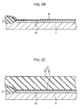
- FIG. 4 is a cross-sectional view showing the conventional semiconductor device.
- An element isolation insulating film 102 is formed on a surface of a substrate 101 , and two field-effect transistors are formed in an element region defined by the element isolation insulating film 102 .
- a tunnel insulating film 103 is formed in each of the transistors, a floating gate 104 , an insulating film 105 , a control gate 106 , a sidewall 107 , a source diffusion layer 141 , and a drain diffusion layer 142 are formed.
- an interlayer insulating film 110 covering the transistors is formed.
- the interlayer insulating film 110 there are formed a contact hole reaching the source diffusion layer 141 and contact holes reaching the drain diffusion layers 142 , and in those contact holes contact plugs 114 are formed. On the interlayer insulating film 110 , wirings 115 contacting the contact plugs 114 are formed. Other interlayer insulating films, wirings and the like are formed (not shown) on the wirings 115 and the like. Incidentally, the source diffusion layer 141 of each transistor is shared by the respective transistors.
- a transistor in which a silicide layer is not formed has been conventionally used as the transistor constituting the memory cell array in view of the cost and the like.
- faster operation and reduced driving voltage are required in such a transistor.
- An object of the present invention is to provide a semiconductor device in which resistance can be reduced even without using a silicide technology, and a manufacturing method of the same.
- a semiconductor device is provided with: a semiconductor substrate; an impurity diffusion layer formed on a surface of the semiconductor substrate; transistors in which the impurity diffusion layer is a source diffusion layer or a drain diffusion layer; an interlayer insulating film covering the transistors; and a contact plug connecting to the impurity diffusion layer and being formed in the interlayer insulating film.
- the semiconductor device is further provided with a conductive film being constituted with the same material as a material constituting the contact plug, and being formed on the impurity diffusion layer.
- a first manufacturing method of a semiconductor device After forming a transistor having a gate electrode, a first impurity diffusion layer and a second impurity diffusion layer on a surface of a semiconductor substrate, a first insulating film covering the transistor is formed. Next, a second insulating film is formed on the first insulating film. Then, the first insulating film is separated into a part of the first impurity diffusion layer side and a part of the second impurity diffusion layer side, with the gate electrode being a boundary. Subsequently, a contact hole reaching the first impurity diffusion layer is formed in the first and the second insulating films. Thereafter, a hollow portion is formed between the first impurity diffusion layer and the second insulating film by removing the first insulating film exposed to the contact hole. Then, a conductive film is formed in the hollow portion.
- a first insulating film which is apart from the second impurity diffusion layer is formed on the first impurity diffusion layer.
- a second insulating film covering the transistor and the first insulating film is formed.
- a contact hole reaching the first impurity diffusion layer is formed in the first and the second insulating films.
- a hollow portion is formed between the first impurity diffusion layer and the second insulating film by removing the first insulating film exposed to the contact hole.
- a conductive film is formed in the hollow portion.
- FIG. 1A to FIG. 1K are cross-sectional views showing a manufacturing method of a semiconductor device according to an embodiment of the present invention step by step;
- FIG. 2A to FIG. 2K are cross-sectional views showing the manufacturing method of a semiconductor device according to the embodiment of the present invention step by step;
- FIG. 3 is a view showing a layout of the semiconductor device according to the embodiment of the present invention.
- FIG. 4 is a cross-sectional view showing a conventional semiconductor device.
- FIG. 1A to FIG. 1K are cross-sectional views showing the manufacturing method of a semiconductor device according to the embodiment of the present invention step by step.
- FIG. 2A to FIG. 2K are also cross-sectional views showing the manufacturing method of a semiconductor device according to the embodiment of the present invention step by step.
- the cross sections shown by FIG. 1A to FIG. 1K and the cross sections shown by FIG. 2A to FIG. 2K are orthogonal to each other.
- FIG. 3 is a view showing a layout of the semiconductor device according to the embodiment of the present invention.
- FIG. 1A to FIG. 1K show the cross sections along a line I-I in FIG. 3
- FIG. 2A to FIG. 2K show the cross sections along a line II-II in FIG. 3 .
- two control gates 6 extend in a first direction, and below the respective control gates 6 a plurality of floating gates 4 are located.
- element isolation insulating films 2 are located between the floating gates 4 next to each other.
- a source diffusion layer (impurity diffusion layer) 41 extending in the first direction is located between the two control gates 6 .
- drain diffusion layers (impurity diffusion layers) 42 are located outside the two floating gates 4 next to each other across the source diffusion layer 41 .
- a contact plug 14 for drain is provided per drain diffusion layer 42 .
- a contact plug 14 for source is provided.
- Sidewalls 7 are located around the control gates 6 .
- a conductive barrier metal film (not shown in FIG. 3 ) is formed in a region between the two sidewalls 7 on the source diffusion layer 41 .
- a manufacturing method for obtaining the structure shown in FIG. 3 will be described.
- a plurality of element active regions are divisionally provided by forming an element isolation insulating film 2 on a surface of a substrate 1 made of p-type silicon or the like, as shown in FIG. 1A and FIG. 2A .
- two transistors are formed in each of the element active regions.
- the transistor there is performed formation of a tunnel insulating film 3 , a floating gate 4 , an insulating film 5 and a control gate 6 , a sidewall 7 , and a source diffusion layer 41 and a drain diffusion layer 42 .
- the source diffusion layer 41 is shared between the two transistors.
- the control gates 6 and the source diffusion layer 41 are shared between the plural transistors next to one another in the first direction.
- a BPSG (Boron Phosphor Silicate Glass) film 8 is formed on an entire surface.
- a thickness of the BPSG film 8 is, for example, about 50 nm.
- a BPSG film 9 is formed on the BPSG film 8 .
- a thickness of the BPSG film 9 is, for example, about 1450 nm.
- the BPSG films 8 and 9 constitute an interlayer insulating film 10 .
- the B concentration in the BPSG film 8 is about five times higher than the B concentration in the BPSG film 9 .
- a heat treatment to the interlayer insulating film 10 is performed until the BPSG film 8 on each transistor flows onto the source diffusion layer 41 or the drain diffusion layer 42 .
- the BPSG film 8 on the source diffusion layer 41 is isolated from the BPSG film 8 located in other regions.
- the BPSG film 8 on the drain diffusion layer 42 is also isolated from the BPSG film 8 located in other regions.
- the BPSG film 8 becomes substantially independent per source diffusion layer 41 and the drain diffusion layer 42 , though the BPSG film 8 slightly remains on an edge portion of the element isolation insulating film 2 .
- a planarization processing of the BPSG film 9 is performed.
- a CMP (Chemical Mechanical Polishing) processing for example, is performed.
- a contact hole 21 reaching the source diffusion layer 41 is formed in the BPSG films 8 and 9 .
- a position in which the contact hole 21 is formed is a position apart from an array of the transistors, as shown in FIG. 2F and FIG. 3 .
- a hollow portion 31 connected to the contact hole 21 is formed as shown in FIG. 1G and FIG. 2G .
- the BPSG film 8 on the drain diffusion layer 42 is not removed, since the BPSG film 8 on the drain diffusion layer 42 is not connected to the BPSG film 8 on the source diffusion layer 41 .
- 0.5% dilute hydrofluoric acid for example, is used.
- the B concentration of the BPSG film 9 is about one fifth of the B concentration of the BPSG film 8 , an etching selection ratio between the BPSG film 8 and the BPSG film 9 is high, and therefore the BPSG film 9 is not removed.
- a contact hole 22 reaching the drain diffusion layer 42 is formed per each drain diffusion layer 42 in the BPSG films 8 and 9 .
- a barrier metal film 12 is formed on the entire surface by, for example, a CVD method.
- the barrier metal film 12 adheres to a surface of the BPSG film 9 , a side surface of the contact hole 21 and a side surface of the contact hole 22 , and is formed also in the hollow portion 31 .
- a thickness of the barrier metal film 12 on the surface of the BPSG film 9 is, for example, about 100 nm.
- a TiN film is formed, for example.
- the hollow portion 31 is filled by the barrier metal film 12 .
- contact plugs 14 made of the barrier metal film 12 and the W film 13 are formed.
- the barrier metal film 12 and the W film 13 are removed until the BPSG film 9 is exposed by a CMP processing or the like, after the W film 13 is formed on the entire surface.
- a conductive contact pad 15 is formed on the contact plug 14 .
- an interlayer insulating film 16 is formed on the entire surface, and the surface thereof is planarized.
- a contact hole reaching the contact pad 15 is formed in the interlayer insulating film 16 .
- conductive contact plugs 17 are embedded in the contact holes exposing the contact pads 15 which are electrically connected to the drain diffusion layers 42
- a conductive contact plug 19 is embedded in the contact hole exposing the contact pad 15 which is electrically connected to the source diffusion layer 41 .
- bit lines 18 connecting the contact plugs 17 next to each other in the second direction are formed on the interlayer insulating film 16 .
- a wiring 20 connected to the contact plug 19 is also formed.
- the conductive barrier metal film 12 made of TiN exists directly on the source diffusion layer 41 . Consequently, resistance between the wiring 20 for source and the source of each transistor is significantly reduced. Therefore, even without adopting a silicide technology, high speed operation and low voltage operation become possible. Moreover, though it is necessary to form a metal film constituting a silicide layer in order to form the silicide layer, a new material is not required in the present embodiment. Further, the number of necessary process steps is smaller compared with the silicide technology. Consequently, a cost increase is smaller compared with the silicide technology.
- the BPSG film 8 may be separated by other processing.
- a CMP processing may be performed until the control gate 6 is exposed, before the BPSG film 9 is formed.
- the BPSG film 8 may be patterned by using a lithography technology and an etching technology, before the BPSG film 9 is formed. In other words, any method can be used as long as the BPSG film 8 can be separated into the part of the source diffusion layer 41 side and the part of the drain diffusion layer 42 side with the gate being a boundary.
- two kinds of insulating films constituting the interlayer insulating film 10 are not limited to the BPSG films. Any film can be used as long as the part directly on the source diffusion layer 41 can be isotropically etched more preferentially than a part thereon. If the BPSG film is used, it is preferable that the B concentration of the film of the lower side is five times or more than the B concentration of the film of the upper side. It is because the etching selection ratio may become small if the B concentration of the film of the lower side is less than five times, and removing only the film of the lower side preferentially may become difficult.
- the conductive film for the purpose of reducing resistance is formed on the source diffusion layer, but the conductive layer can be formed on the drain diffusion layer as necessary. This is effective when the drain diffusion layer is shared between plural transistors.
- a conductive film exists on an impurity diffusion layer resistance can be reduced even without adopting a silicide technology. As a result, faster operation and reduced operational voltage become possible also in a semiconductor device in which the silicide technology is not adopted.
Landscapes
- Semiconductor Memories (AREA)
- Internal Circuitry In Semiconductor Integrated Circuit Devices (AREA)
- Electrodes Of Semiconductors (AREA)
- Non-Volatile Memory (AREA)
Abstract
Description
Claims (21)
Applications Claiming Priority (2)
| Application Number | Priority Date | Filing Date | Title |
|---|---|---|---|
| JP2006081480A JP2007258481A (en) | 2006-03-23 | 2006-03-23 | Semiconductor device and manufacturing method thereof |
| JP2006-081480 | 2006-03-23 |
Publications (2)
| Publication Number | Publication Date |
|---|---|
| US20070224802A1 US20070224802A1 (en) | 2007-09-27 |
| US7611983B2 true US7611983B2 (en) | 2009-11-03 |
Family
ID=38534036
Family Applications (1)
| Application Number | Title | Priority Date | Filing Date |
|---|---|---|---|
| US11/513,029 Expired - Fee Related US7611983B2 (en) | 2006-03-23 | 2006-08-31 | Semiconductor device and a manufacturing method of the same |
Country Status (2)
| Country | Link |
|---|---|
| US (1) | US7611983B2 (en) |
| JP (1) | JP2007258481A (en) |
Families Citing this family (2)
| Publication number | Priority date | Publication date | Assignee | Title |
|---|---|---|---|---|
| US8110877B2 (en) * | 2008-12-19 | 2012-02-07 | Intel Corporation | Metal-insulator-semiconductor tunneling contacts having an insulative layer disposed between source/drain contacts and source/drain regions |
| US8232627B2 (en) * | 2009-09-21 | 2012-07-31 | International Business Machines Corporation | Integrated circuit device with series-connected field effect transistors and integrated voltage equalization and method of forming the device |
Citations (6)
| Publication number | Priority date | Publication date | Assignee | Title |
|---|---|---|---|---|
| JPH08274066A (en) | 1995-03-29 | 1996-10-18 | Matsushita Electric Works Ltd | Formation of contact window |
| JPH09148434A (en) | 1995-11-29 | 1997-06-06 | Hitachi Ltd | Wiring interlayer connection method |
| JPH1050835A (en) | 1996-08-06 | 1998-02-20 | Ricoh Co Ltd | Semiconductor device and method of manufacturing semiconductor device |
| JP2000195950A (en) | 1998-12-28 | 2000-07-14 | Nec Corp | Semiconductor device and manufacturing method thereof |
| US20020197816A1 (en) * | 1998-11-12 | 2002-12-26 | Deboer Scott J. | Structural integrity enhancement of dielectric films |
| JP2003197739A (en) | 2001-12-13 | 2003-07-11 | Samsung Electronics Co Ltd | Semiconductor device and method of forming the same |
Family Cites Families (6)
| Publication number | Priority date | Publication date | Assignee | Title |
|---|---|---|---|---|
| US2767126A (en) * | 1953-03-23 | 1956-10-16 | Gulf Research Development Co | Catalytic cracking process and apparatus |
| FR2584732B1 (en) * | 1985-07-10 | 1988-08-19 | Raffinage Cie Francaise | PROCESS AND DEVICE FOR THE CATALYTIC CRACKING OF HYDROCARBON CHARGES, WITH CONTROL OF THE REACTION TEMPERATURE |
| US4874503A (en) * | 1988-01-15 | 1989-10-17 | Mobil Oil Corporation | Multiple riser fluidized catalytic cracking process employing a mixed catalyst |
| US6156189A (en) * | 1998-04-28 | 2000-12-05 | Exxon Research And Engineering Company | Operating method for fluid catalytic cracking involving alternating feed injection |
| JP2001127151A (en) * | 1999-10-26 | 2001-05-11 | Fujitsu Ltd | Semiconductor device and method of manufacturing the same |
| JP2004266082A (en) * | 2003-02-28 | 2004-09-24 | Mitsumi Electric Co Ltd | Semiconductor device manufacturing method and semiconductor device |
-
2006
- 2006-03-23 JP JP2006081480A patent/JP2007258481A/en active Pending
- 2006-08-31 US US11/513,029 patent/US7611983B2/en not_active Expired - Fee Related
Patent Citations (6)
| Publication number | Priority date | Publication date | Assignee | Title |
|---|---|---|---|---|
| JPH08274066A (en) | 1995-03-29 | 1996-10-18 | Matsushita Electric Works Ltd | Formation of contact window |
| JPH09148434A (en) | 1995-11-29 | 1997-06-06 | Hitachi Ltd | Wiring interlayer connection method |
| JPH1050835A (en) | 1996-08-06 | 1998-02-20 | Ricoh Co Ltd | Semiconductor device and method of manufacturing semiconductor device |
| US20020197816A1 (en) * | 1998-11-12 | 2002-12-26 | Deboer Scott J. | Structural integrity enhancement of dielectric films |
| JP2000195950A (en) | 1998-12-28 | 2000-07-14 | Nec Corp | Semiconductor device and manufacturing method thereof |
| JP2003197739A (en) | 2001-12-13 | 2003-07-11 | Samsung Electronics Co Ltd | Semiconductor device and method of forming the same |
Also Published As
| Publication number | Publication date |
|---|---|
| US20070224802A1 (en) | 2007-09-27 |
| JP2007258481A (en) | 2007-10-04 |
Similar Documents
| Publication | Publication Date | Title |
|---|---|---|
| US11508614B2 (en) | Method of forming semiconductor device having capped air gaps between buried bit lines and buried gate | |
| KR100936585B1 (en) | Semiconductor device and manufacturing method thereof | |
| KR102796606B1 (en) | Semiconductor device | |
| CN100550385C (en) | Method and structure of self-aligned device contacts | |
| US9627316B1 (en) | Field effect transistor devices having interconnect structures and manufacturing method thereof | |
| US20200066683A1 (en) | Semiconductor device and method of fabricating the same | |
| TWI708392B (en) | Fdsoi semiconductor device with contact enhancement layer and method of manufacturing | |
| US20120091518A1 (en) | Semiconductor device, method for forming the same, and data processing system | |
| CN108063139A (en) | Semiconductor device | |
| JPH11186518A (en) | Semiconductor integrated circuit device and method of manufacturing the same | |
| KR20170033494A (en) | Semiconductor devices and methods of manufacturing semiconductor devices | |
| JPH11204753A (en) | Method of manufacturing semiconductor integrated circuit device and semiconductor integrated circuit device | |
| US6809381B2 (en) | Semiconductor memory device having full depletion type logic transistors and partial depletion type memory transistors | |
| CN117062436A (en) | Semiconductor memory device and manufacturing method thereof | |
| JP2009152361A (en) | Semiconductor device and manufacturing method thereof | |
| US20110147889A1 (en) | Semiconductor device and method of manufacturing semiconductor device | |
| JP5294604B2 (en) | Nonvolatile memory device and method of forming the same | |
| KR20100018156A (en) | A stacked semiconductor device and method of manufacturing the same | |
| US20130193516A1 (en) | Sram integrated circuits and methods for their fabrication | |
| US10269811B2 (en) | Selective SAC capping on fin field effect transistor structures and related methods | |
| US7611983B2 (en) | Semiconductor device and a manufacturing method of the same | |
| US12142519B2 (en) | Etch stop detection structure and etch stop detection method | |
| JP2009164534A (en) | Semiconductor device and manufacturing method therefor | |
| JP2000138357A (en) | Method of manufacturing semiconductor integrated circuit device and semiconductor integrated circuit device | |
| US8119493B2 (en) | Method of forming a semiconductor device an alignment mark formed in a groove |
Legal Events
| Date | Code | Title | Description |
|---|---|---|---|
| AS | Assignment |
Owner name: FUJITSU LIMITED, JAPAN Free format text: ASSIGNMENT OF ASSIGNORS INTEREST;ASSIGNOR:NISHIMURA, AKIHITO;REEL/FRAME:018256/0116 Effective date: 20060718 |
|
| AS | Assignment |
Owner name: FUJITSU MICROELECTRONICS LIMITED, JAPAN Free format text: ASSIGNMENT OF ASSIGNORS INTEREST;ASSIGNOR:FUJITSU LIMITED;REEL/FRAME:021976/0089 Effective date: 20081104 Owner name: FUJITSU MICROELECTRONICS LIMITED,JAPAN Free format text: ASSIGNMENT OF ASSIGNORS INTEREST;ASSIGNOR:FUJITSU LIMITED;REEL/FRAME:021976/0089 Effective date: 20081104 |
|
| FEPP | Fee payment procedure |
Free format text: PAYOR NUMBER ASSIGNED (ORIGINAL EVENT CODE: ASPN); ENTITY STATUS OF PATENT OWNER: LARGE ENTITY |
|
| AS | Assignment |
Owner name: FUJITSU SEMICONDUCTOR LIMITED, JAPAN Free format text: CHANGE OF NAME;ASSIGNOR:FUJITSU MICROELECTRONICS LIMITED;REEL/FRAME:025046/0478 Effective date: 20100401 |
|
| REMI | Maintenance fee reminder mailed | ||
| LAPS | Lapse for failure to pay maintenance fees | ||
| STCH | Information on status: patent discontinuation |
Free format text: PATENT EXPIRED DUE TO NONPAYMENT OF MAINTENANCE FEES UNDER 37 CFR 1.362 |
|
| STCH | Information on status: patent discontinuation |
Free format text: PATENT EXPIRED DUE TO NONPAYMENT OF MAINTENANCE FEES UNDER 37 CFR 1.362 |
|
| FP | Lapsed due to failure to pay maintenance fee |
Effective date: 20131103 |